Power Loss Reduction of Angled Metallic Wedge Plasmonic Waveguides via the Interplay between Near-Field Optical Coupling and Modal Coupling

 , and
, and 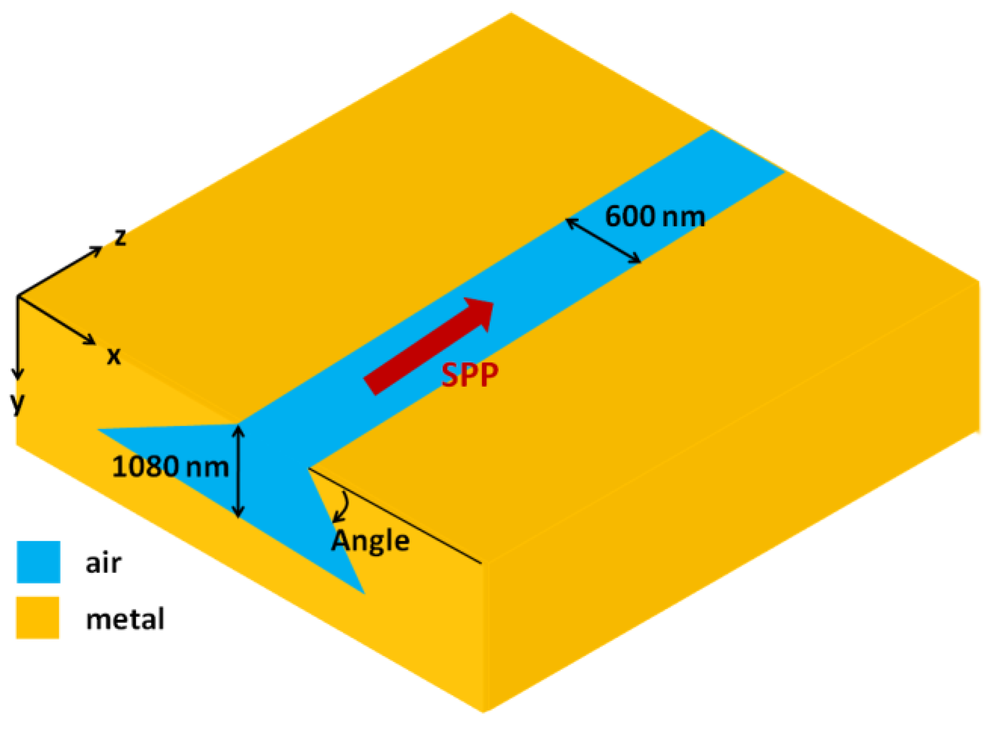
Abstract
:1. Introduction
2. Simulation Layout and Methodology
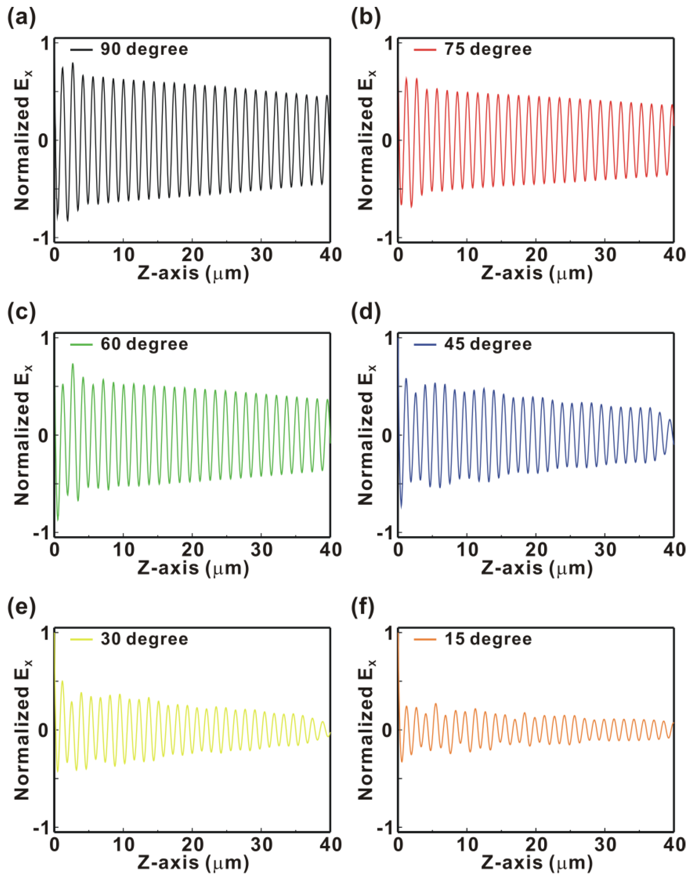
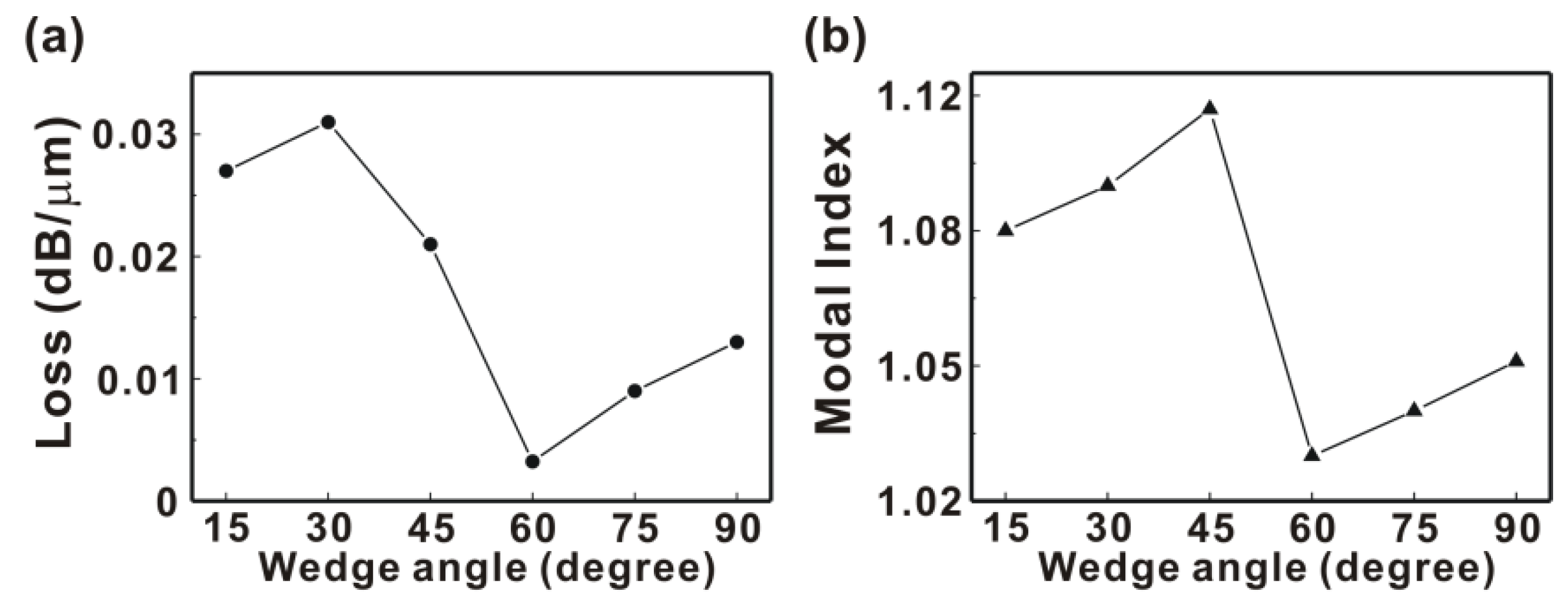
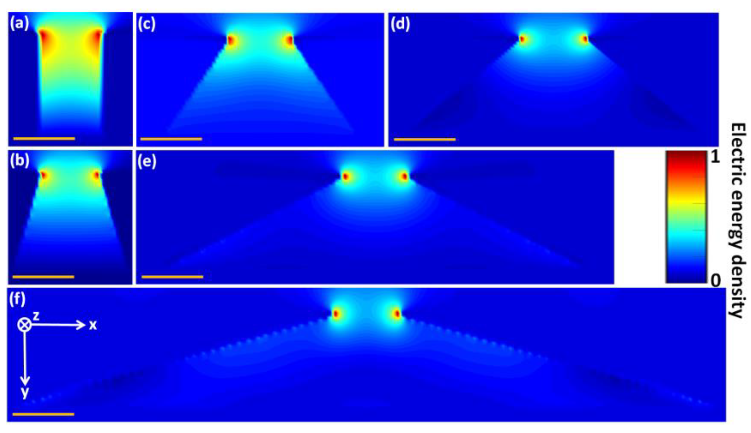
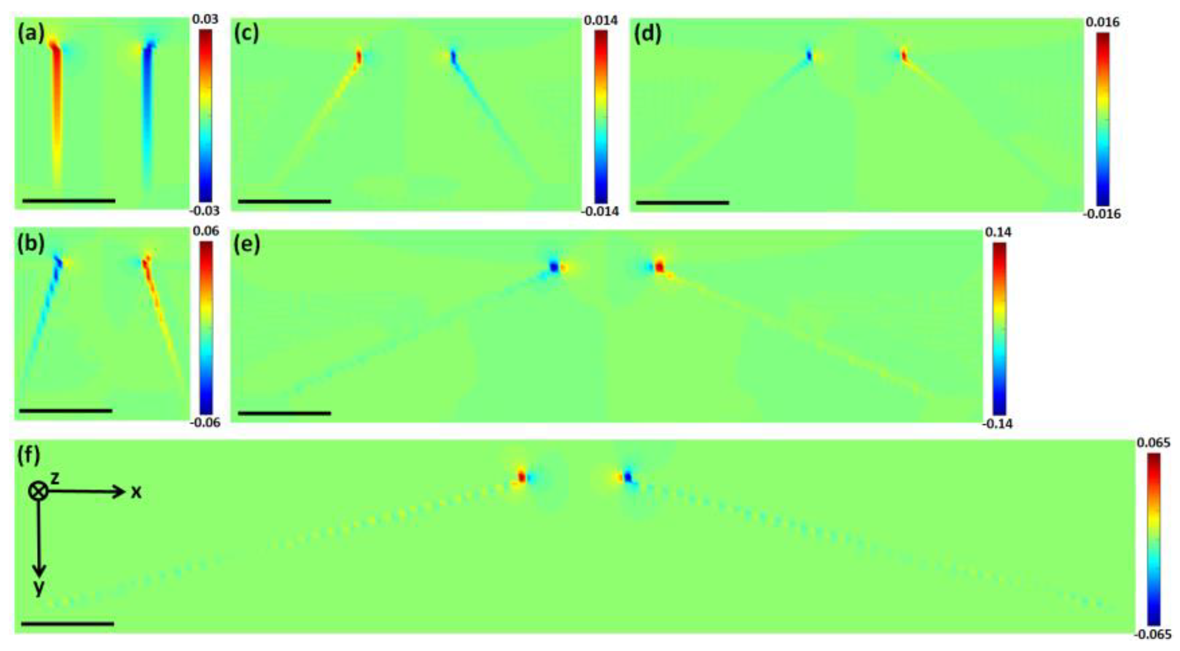
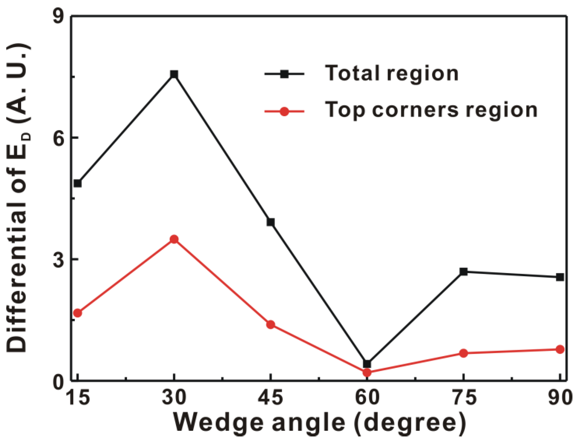
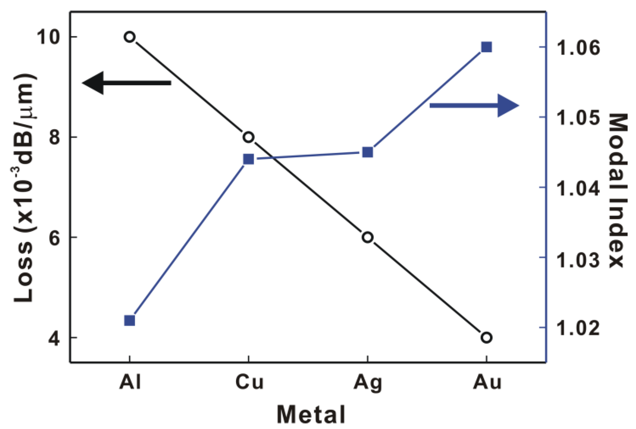
3. Results and Discussion
4. Conclusions
Supplementary Materials
Author Contributions
Funding
Institutional Review Board Statement
Informed Consent Statement
Data Availability Statement
Conflicts of Interest
References
- Chang, S.H. Modeling and design of Ag, Au, and Cu nanoplasmonic structures for enhancing the absorption of P3HT:PCBM based photovoltaics. IEEE Photonics J. 2013, 5, 48000509. [Google Scholar]
- Yu, H.; Peng, Y.; Yang, Y.; Li, Z.Y. Plasmon-enhanced light-matter interactions and applications. NPJ Comput. Mater. 2019, 5, 45. [Google Scholar] [CrossRef]
- Ning, X.; Yin, D.; Fan, Y.; Zhang, Q.; Du, P.; Zhang, D.; Chen, J.; Lu, X. Plasmon-enhanced charge separation and surface reactions based on Ag-loaded transition-metal hydroxide for photoelectrochemical water oxidation. Adv. Energy Mater. 2021, 11, 2100405. [Google Scholar] [CrossRef]
- Oulton, R.F.; Bartal, G.; Pile, D.F.P.; Zhang, X. Confinement and propagation characteristics of subwavelength plasmonic modes. New J. Phys. 2008, 10, 105018. [Google Scholar] [CrossRef]
- Gjerding, M.N.; Pandey, M.; Thygesen, K.S. Band structure engineered layered metals for low-loss plasmonics. Nat. Commun. 2017, 8, 15133. [Google Scholar] [CrossRef]
- Bozhevolnyi, S.I. Effective-index modeling of channel plasmon polaritons. Opt. Express 2006, 14, 9467–9476. [Google Scholar] [CrossRef]
- Feigenbaum, E.; Orenstein, M. Nano plasmon polariton modes of a wedge cross section metal waveguide. Opt. Express 2006, 14, 8779–8784. [Google Scholar] [CrossRef]
- Sheikhi, K.; Granpayeh, N. Lossless propagation in active channel plasmon polariton. Opt. Commun. 2014, 322, 73–77. [Google Scholar] [CrossRef]
- Chang, S.H.; Chiu, T.; Tai, C.Y. Propagation characteristics of the supermode based on two coupled semi-infinite rib plasmonic waveguides. Opt. Express 2007, 15, 1755–1761. [Google Scholar] [CrossRef]
- Liu, P.; Zhang, X.; Ma, Z.; Cai, W.; Wang, L.; Xu, J. Surface plasmon modes in grapheme wedge and groove waveguides. Opt. Express 2013, 21, 32432–32440. [Google Scholar] [CrossRef]
- Tai, C.Y.; Yu, W.S. Orders of magnitude enhancement of mode splitting by plasmonic intracavity resonance. Opt. Express 2012, 20, 22172–22180. [Google Scholar] [CrossRef] [PubMed]
- Chung, S.Y.; Wang, C.Y.; Teng, C.H.; Chen, C.P.; Chang, H.C. Simulations of dielectric and plasmonic waveguide-coupled ring resonators using the legendrepseudospectral time-domain method. J. Lightwave Technol. 2012, 30, 1733–1742. [Google Scholar] [CrossRef]
- Kamada, S.; Okamoto, T.; Haraguchi, M. Size-dependent plasmonic resonance of rectangular resonator coupled with plasmonic waveguide. Appl. Phys. Lett. 2019, 114, 063102. [Google Scholar] [CrossRef]
- Shamy, R.S.E.; Khalil, D.; Swillam, M.A. Mid infrared optical gas sensor using plasmonic Mach-Zehnder Interferometer. Sci. Rep. 2020, 10, 1293. [Google Scholar] [CrossRef]
- Voronin, K.V.; Stebunov, Y.V.; Voronov, A.A.; Arsenin, A.V.; Volkov, V.S. Vertically coupled plasmonic racetrack ring resonator for biosensor applications. Sensors 2020, 20, 203. [Google Scholar] [CrossRef] [PubMed]
- Wu, T.; Liu, Y.; Yu, Z.; Peng, Y.; Shu, C.; Ye, H. The sensing characteristics of plasmonic waveguide with a ring resonator. Opt. Express 2014, 22, 7669–7677. [Google Scholar] [CrossRef] [PubMed]
- Khonina, S.N.; Kazanskiy, N.L.; Butt, M.A.; Kazmierczak, A.; Piramidowicz, R. Plasmonic sensor based on metal-insulator-metal waveguide square ring cavity filled with functional material for the detection of CO2 gas. Opt. Express 2021, 29, 16584–16594. [Google Scholar] [CrossRef] [PubMed]
- Khattak, A.; Wei, L. Fano resonance hybrid waveguide-coupled plasmonic sensor using transparent conductive oxide in the near-infrared range. Photonics 2022, 9, 189. [Google Scholar] [CrossRef]
- Offermans, P.; Schaafsma, M.C.; Rodriguez, S.R.K.; Zhang, Y.; Crego-Calama, M.; Brongersma, S.H.; Rivas, J.G. Universal Scaling of the figure of merit of plasmonic sensors. ACS Nano 2011, 5, 5151–5157. [Google Scholar] [CrossRef]
- Couture, M.; Brule, T.; Laing, S.; Cui, W.; Sarkar, M.; Charron, B.; Faulds, K.; Peng, W.; Canva, M.; Masson, J.-F. High figure of merit (FOM) of Bragg modes in Au-coated arrays for plasmonic sensing. Small 2017, 13, 1700908. [Google Scholar] [CrossRef]
- Meng, Q.-Q.; Zhao, X.; Lin, C.-Y.; Chen, S.-J.; Ding, Y.-C.; Chen, Z.-Y. Figure of merit enhancement of a surface plasmon resonance sensor using a low-refractive-index porous silica film. Sensors 2017, 17, 1846. [Google Scholar] [CrossRef] [PubMed] [Green Version]
- Liao, Y.S.; Lee, P.H.; Shen, H.Q.; Wu, J.R.; Chang, S.H. Wedge angle-dependent propagation characteristics of two coupled semi-infinite Au rib nanoplasmonics waveguides. Plasmonics 2021, 16, 227–232. [Google Scholar] [CrossRef]
- Kaminow, I.P. Optical integrated circuits: A personal perspective. IEEE J. Lightwave Technol. 2008, 26, 994–1004. [Google Scholar] [CrossRef]
- Patri, A.; Kena-Cohen, S.; Caloz, C. Large-angle, broadband, and multifunctional directive waveguide scatterer gratings. ACS Photonics 2019, 6, 3298–3305. [Google Scholar] [CrossRef]
- Li, X.; Jiang, T.; Shen, L.; Deng, X. Subwavelength guiding of channel Plasmon polaritons by textured metallic grooves at telecom wavelengths. Appl. Phys. Lett. 2013, 102, 031606. [Google Scholar] [CrossRef]
- Mazzone, V.; Gongora, J.S.T.; Fratalocchi, A. Near-field coupling and mode competition in multiple anapole systems. Appl. Sci. 2017, 7, 542. [Google Scholar] [CrossRef]
- Esmann, M.; Becker, S.F.; Witt, J.; Zhan, J.; Chimeh, A.; Korte, A.; Zhong, J.; Vogelgesang, R.; Wittstock, G.; Lienau, C. Vectorial near-field coupling. Nat. Nanotechnol. 2019, 14, 698–704. [Google Scholar] [CrossRef]
- Chen, Y.T.; Chandel, A.; Wu, J.R.; Chang, S.H. Coupled periodically electric quadrupoles assisted ultra-broadband light-extraction enhancement of red GaN LEDs by manipulating the field orthogonality at nanoscales. Chin. J. Phys. 2021, 70, 188–195. [Google Scholar] [CrossRef]
- Pakic, A.D.; Djurisic, A.B.; Elazar, J.M.; Majewski, M.L. Optical properties of metallic films for vertical-cavity optoelectronic devices. Appl. Opt. 1998, 37, 5271–5283. [Google Scholar]


Publisher’s Note: MDPI stays neutral with regard to jurisdictional claims in published maps and institutional affiliations. |
© 2022 by the authors. Licensee MDPI, Basel, Switzerland. This article is an open access article distributed under the terms and conditions of the Creative Commons Attribution (CC BY) license (https://creativecommons.org/licenses/by/4.0/).
Share and Cite
Liao, Y.-S.; Wu, J.-R.; Thakur, D.; Hsu, J.-S.; Dwivedi, R.P.; Chang, S.H. Power Loss Reduction of Angled Metallic Wedge Plasmonic Waveguides via the Interplay between Near-Field Optical Coupling and Modal Coupling. Photonics 2022, 9, 663. https://doi.org/10.3390/photonics9090663
Liao Y-S, Wu J-R, Thakur D, Hsu J-S, Dwivedi RP, Chang SH. Power Loss Reduction of Angled Metallic Wedge Plasmonic Waveguides via the Interplay between Near-Field Optical Coupling and Modal Coupling. Photonics. 2022; 9(9):663. https://doi.org/10.3390/photonics9090663
Chicago/Turabian StyleLiao, Yin-Song, Jia-Ren Wu, Diksha Thakur, Jy-Shan Hsu, Ram Prakash Dwivedi, and Sheng Hsiung Chang. 2022. "Power Loss Reduction of Angled Metallic Wedge Plasmonic Waveguides via the Interplay between Near-Field Optical Coupling and Modal Coupling" Photonics 9, no. 9: 663. https://doi.org/10.3390/photonics9090663