Polarization-Insensitive Graphene Modulator Based on Hybrid Plasmonic Waveguide

 , and
, and
Abstract
:1. Introduction
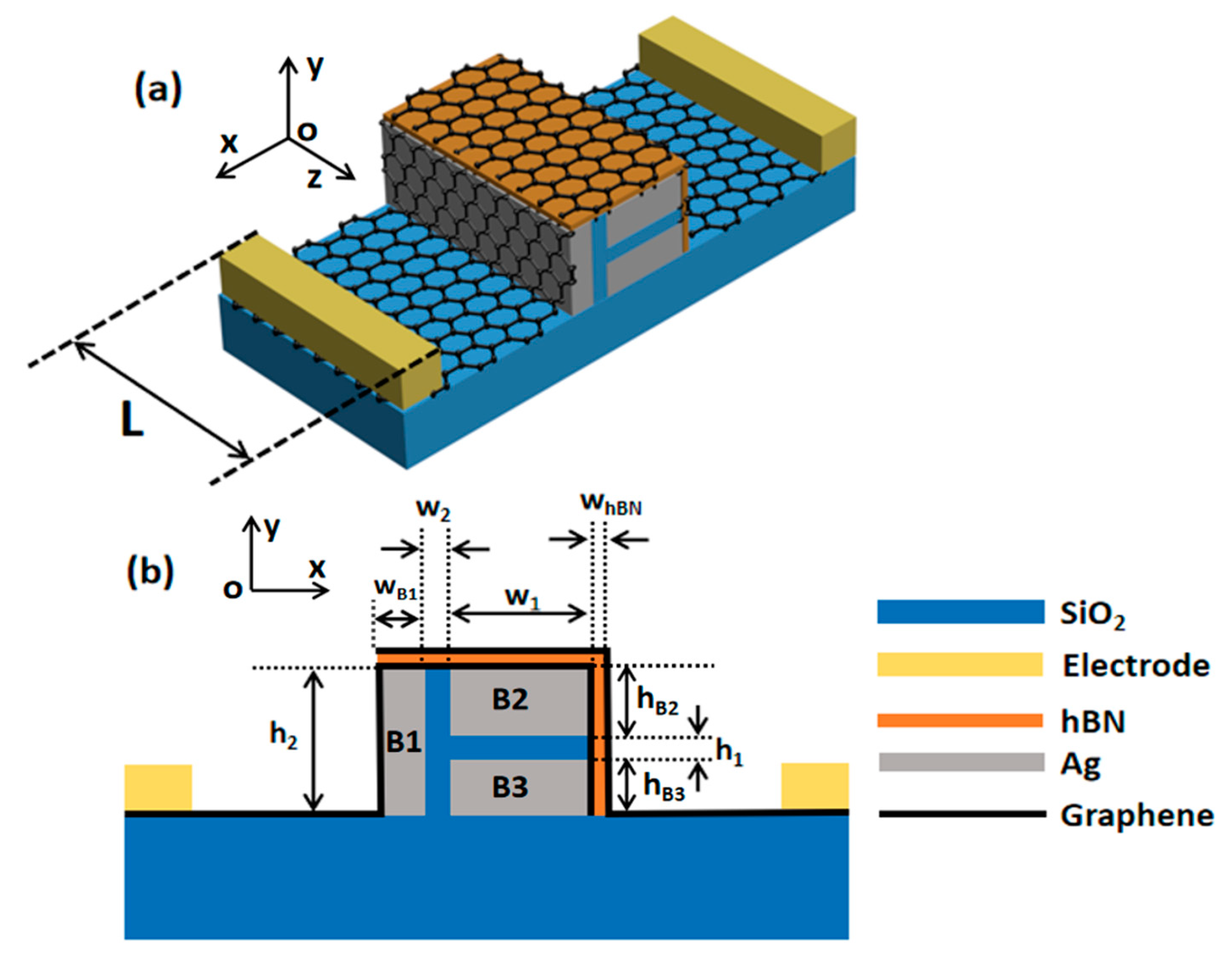
2. Device Structure
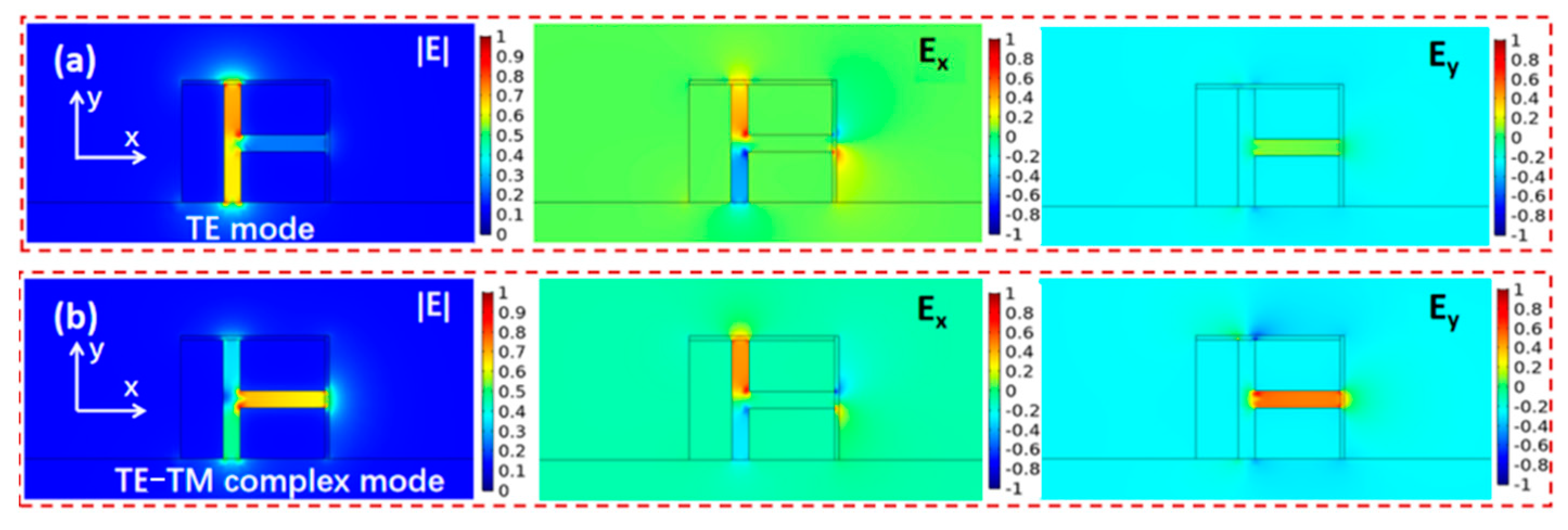
2.1. Hybrid Plasmonic Slot Waveguide
2.2. Graphene Film
3. Design and Optimization
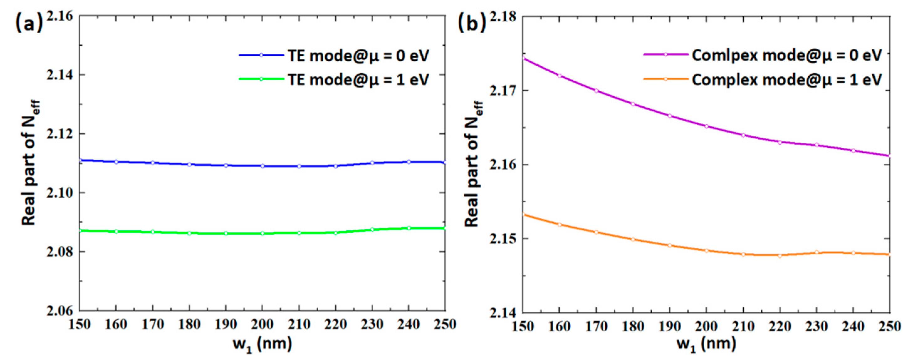
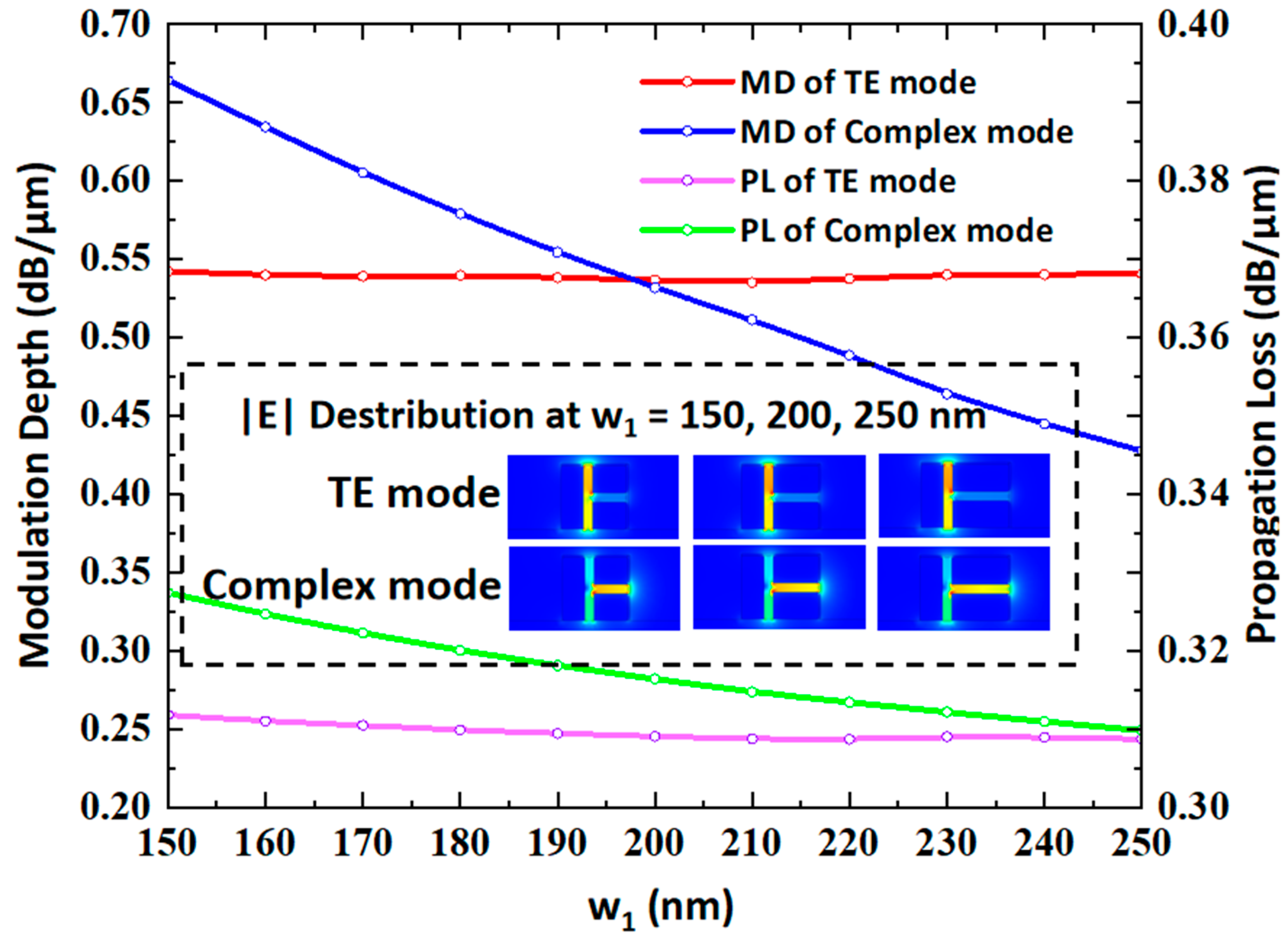
3.1. w1
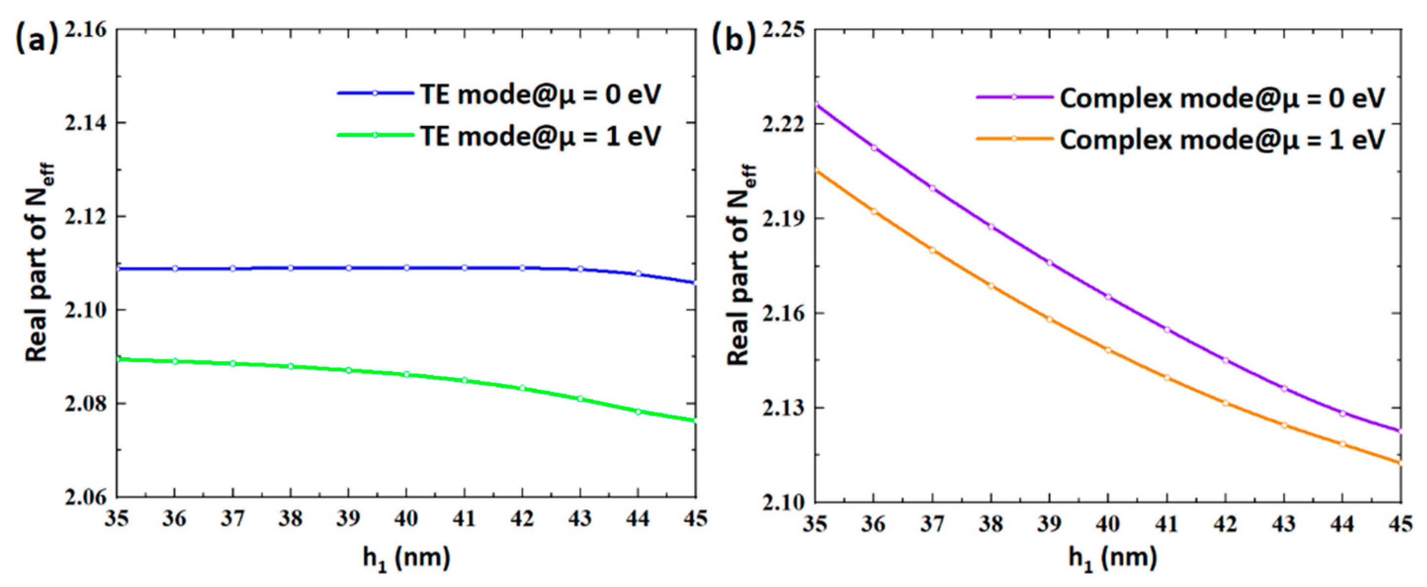
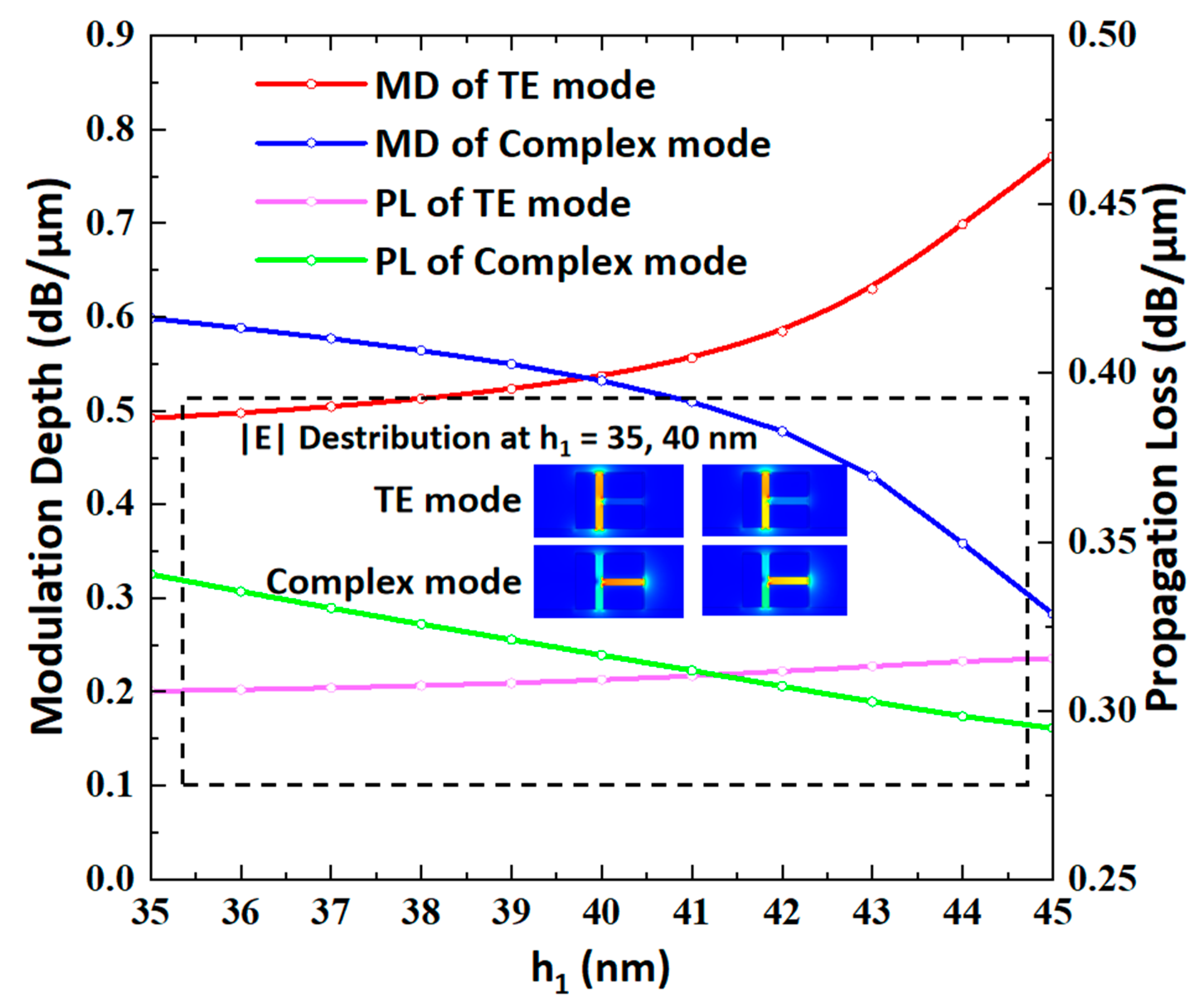
3.2. h1
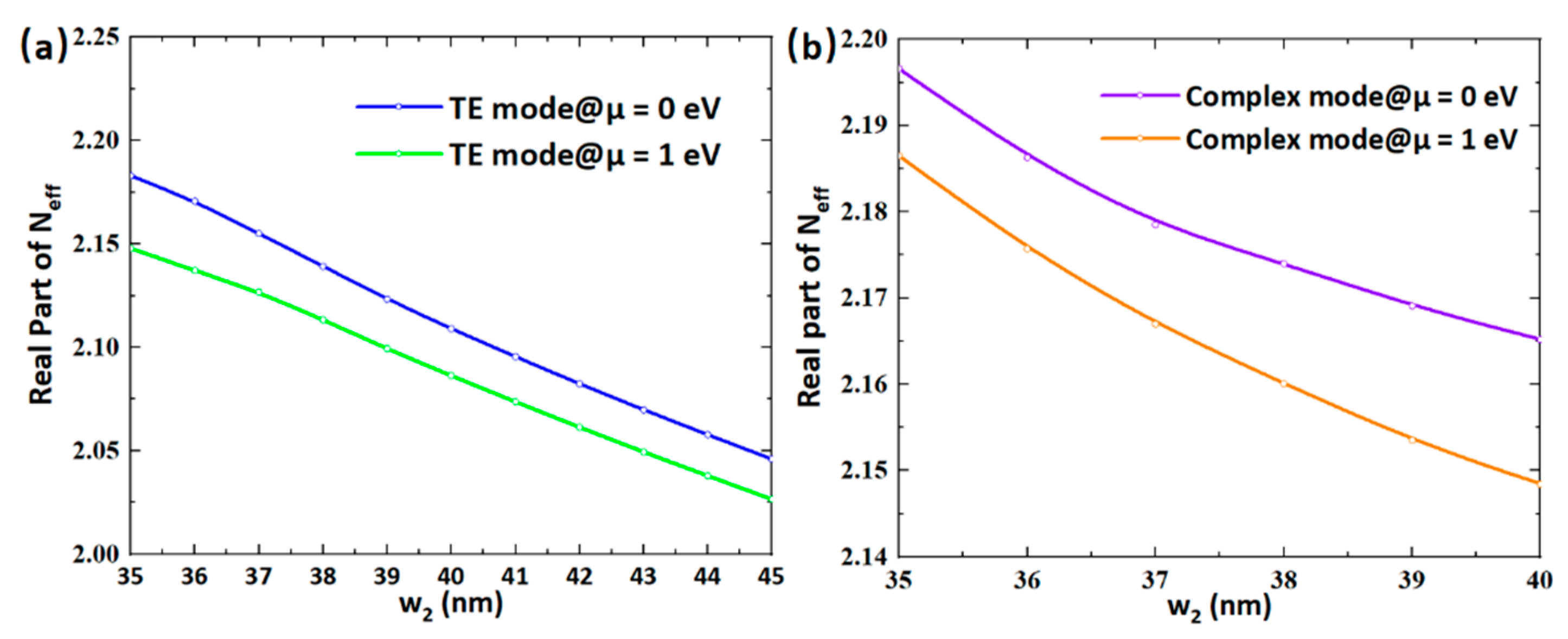
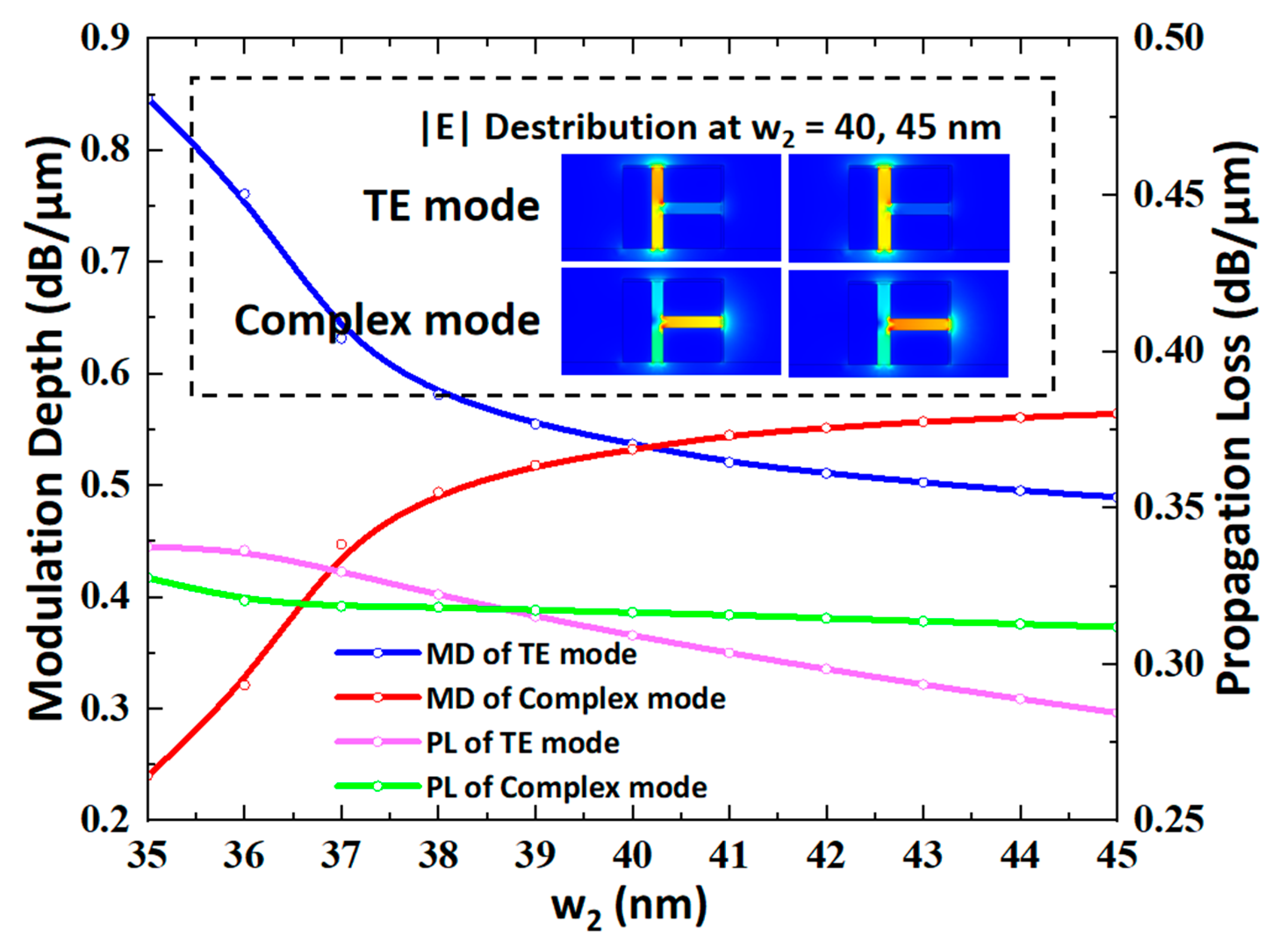
3.3. w2
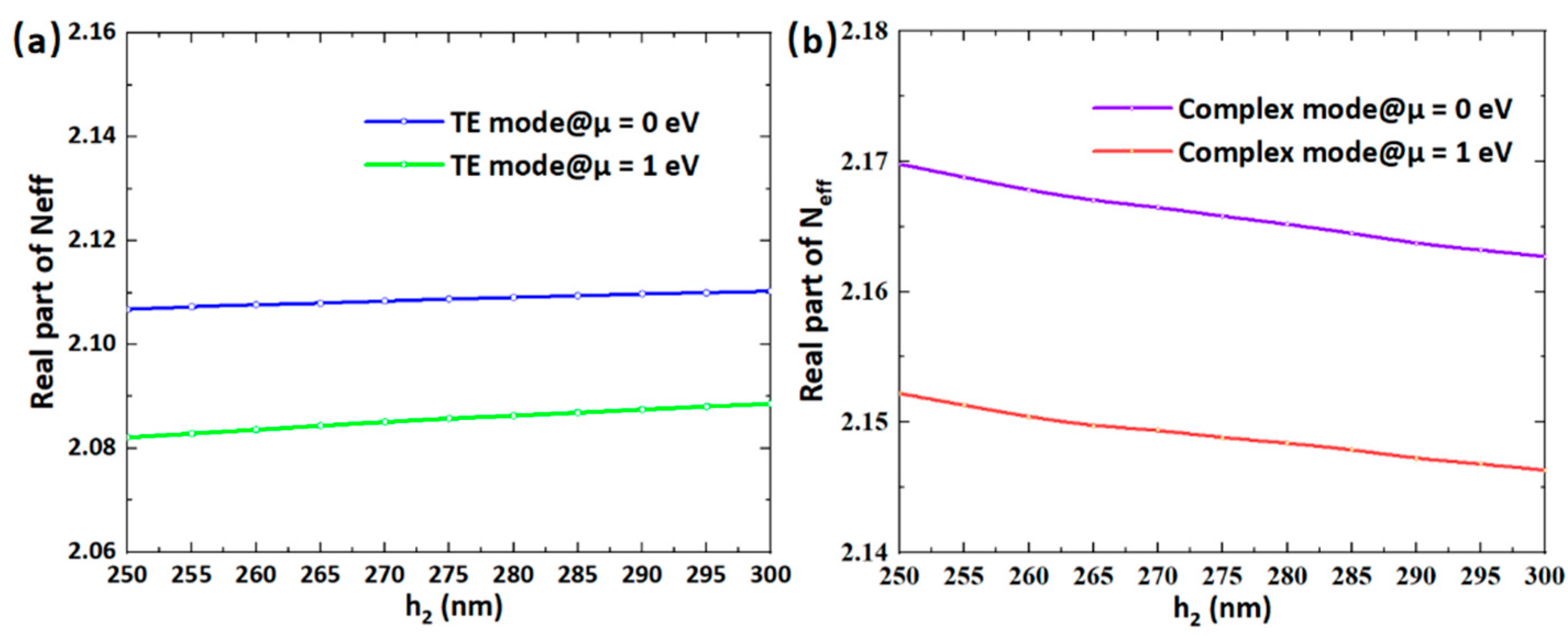
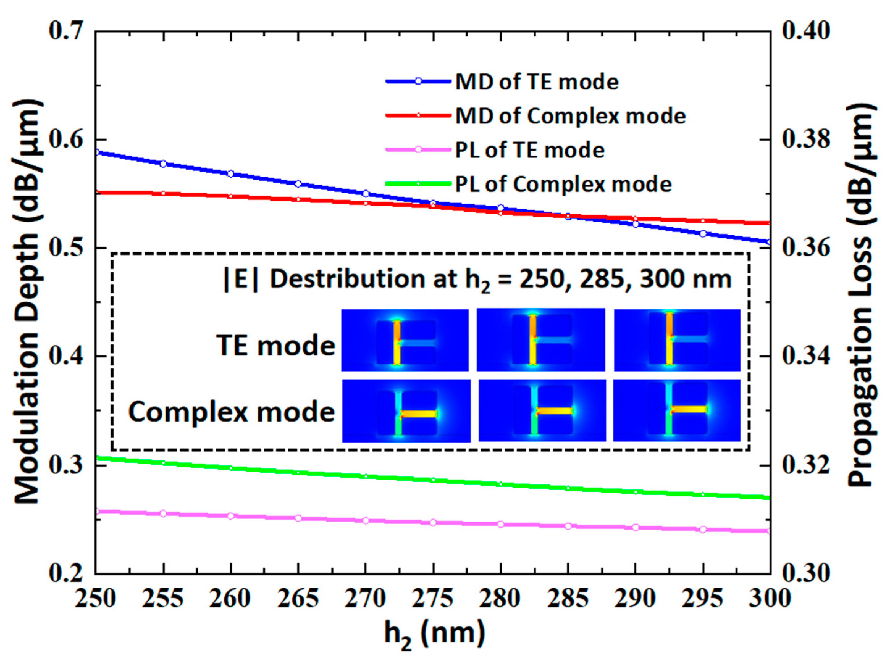
3.4. h2
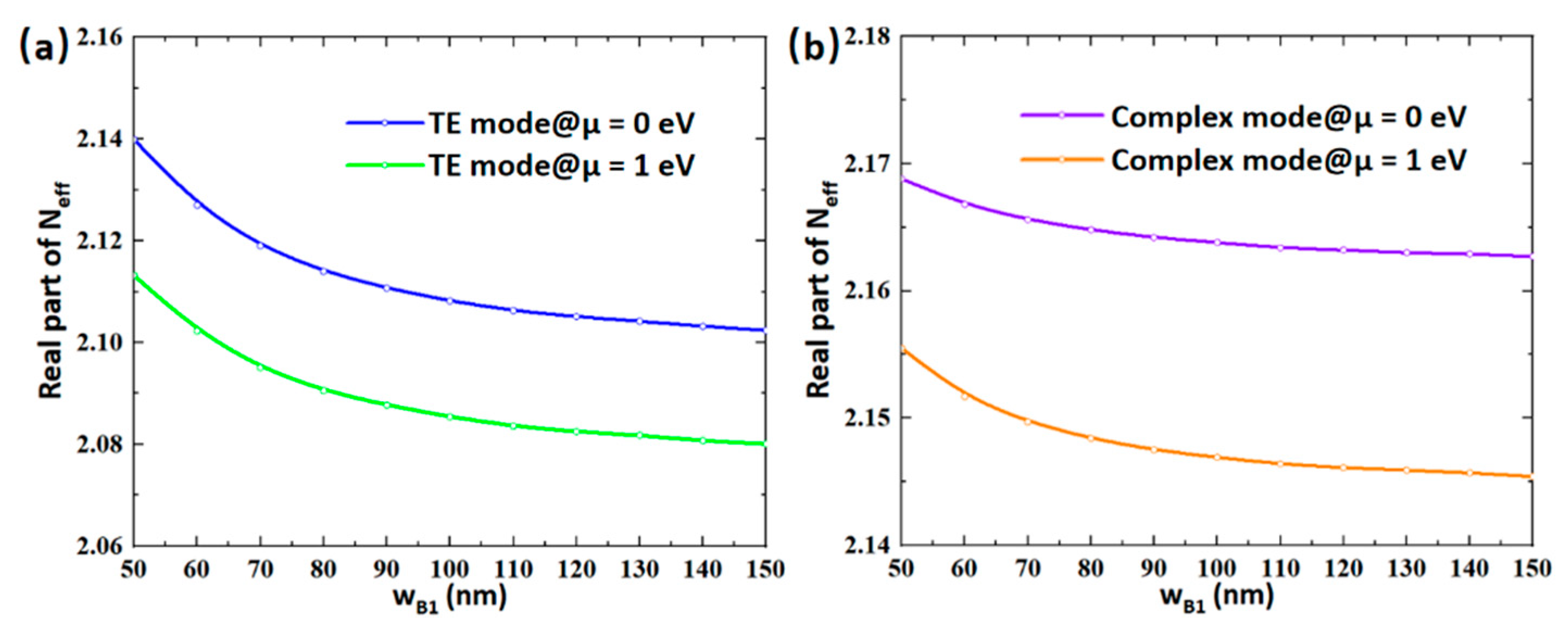
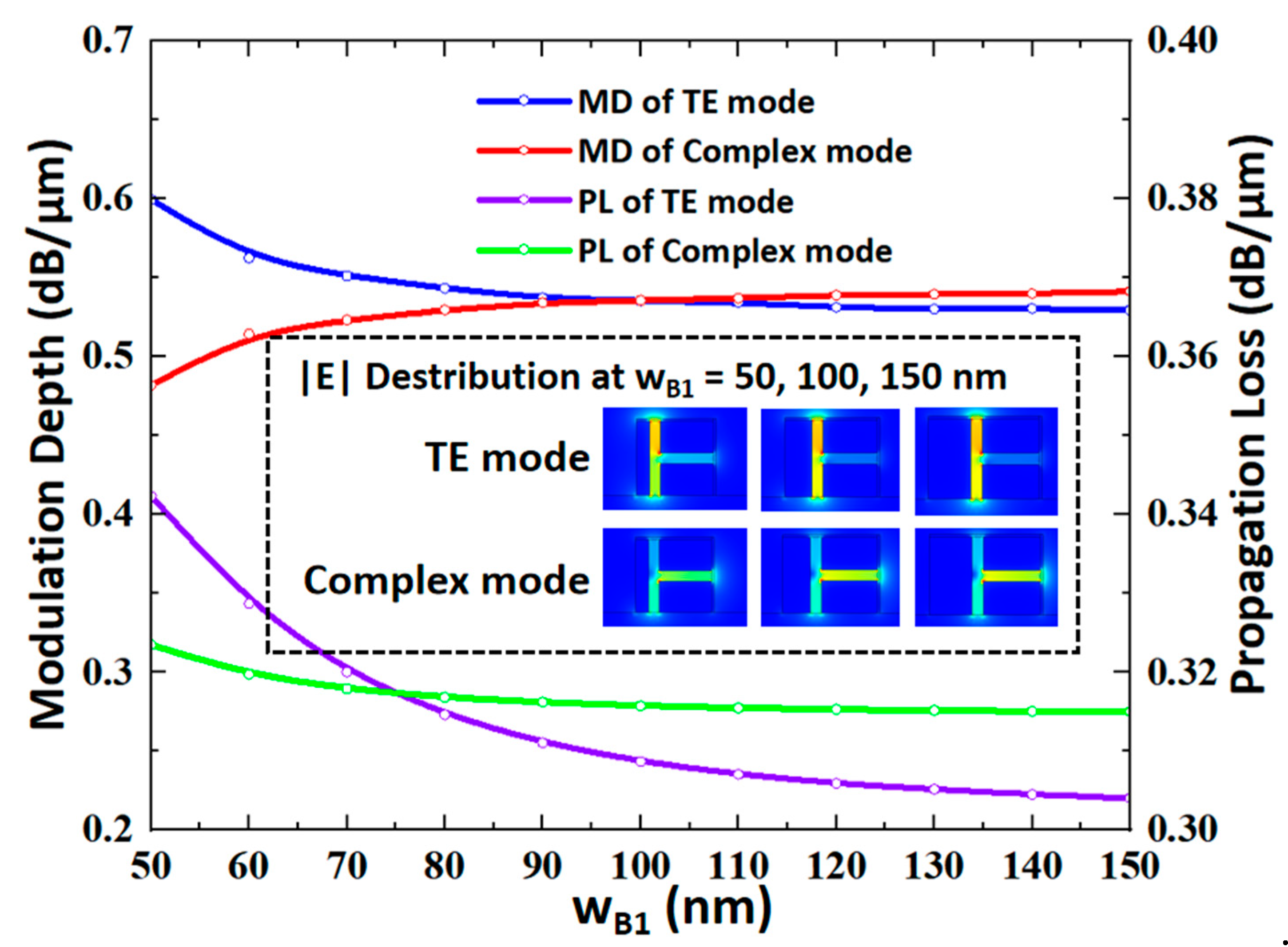
3.5. wB1
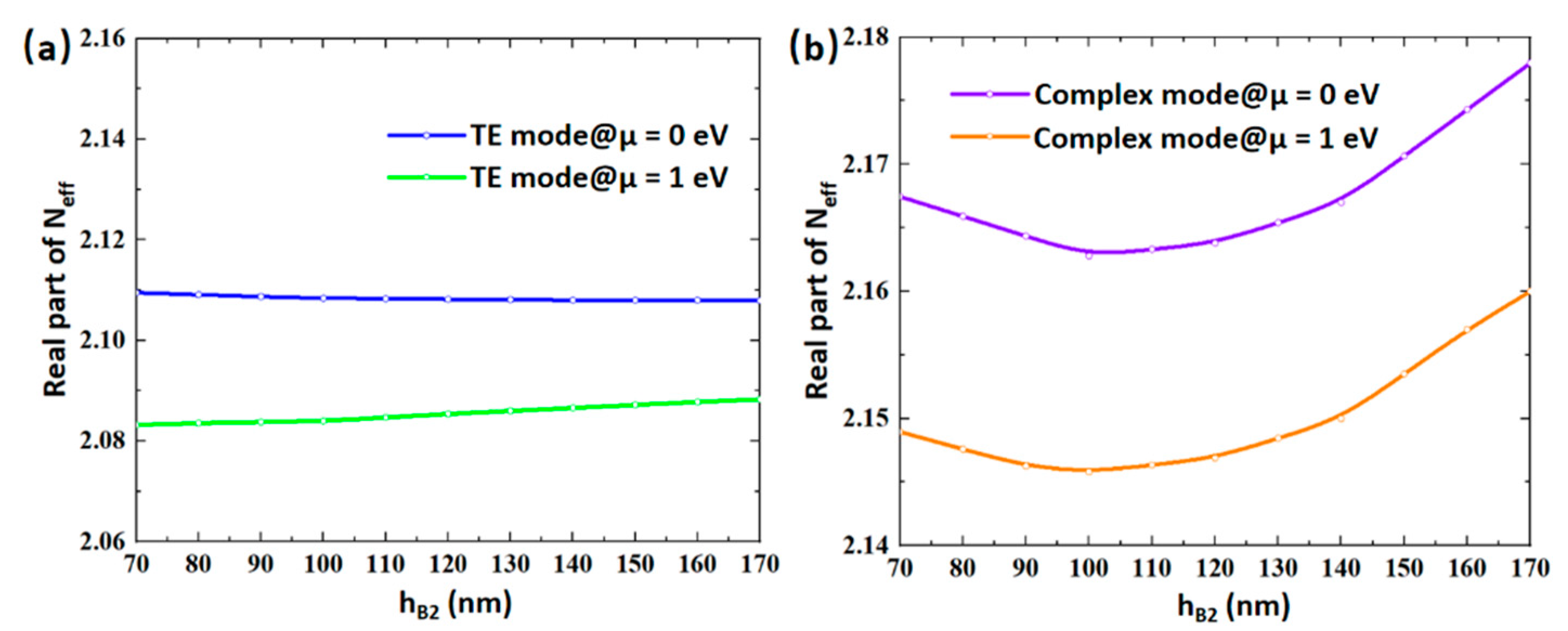
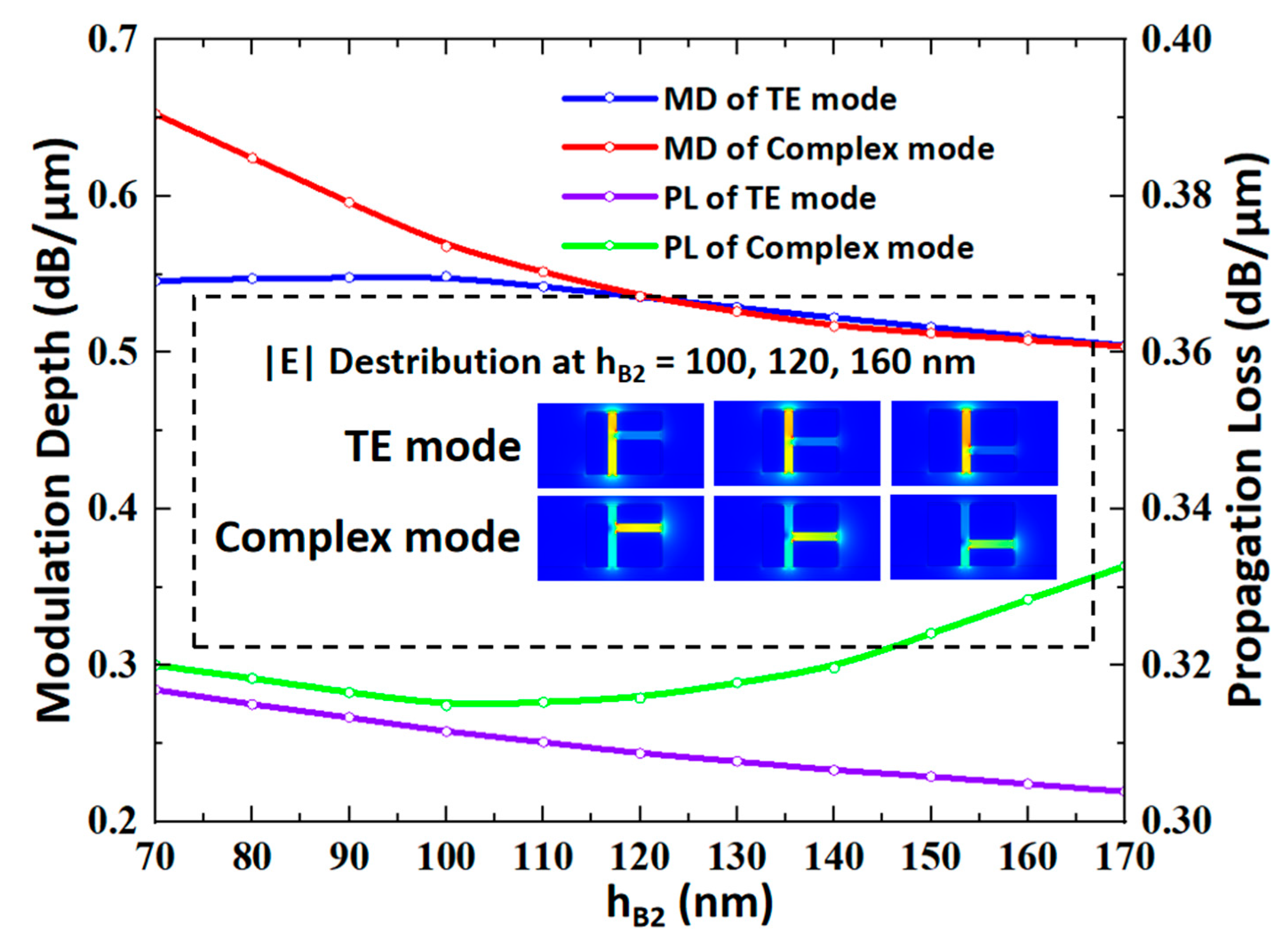
3.6. hB2 and hB3
4. Performance and Discussion
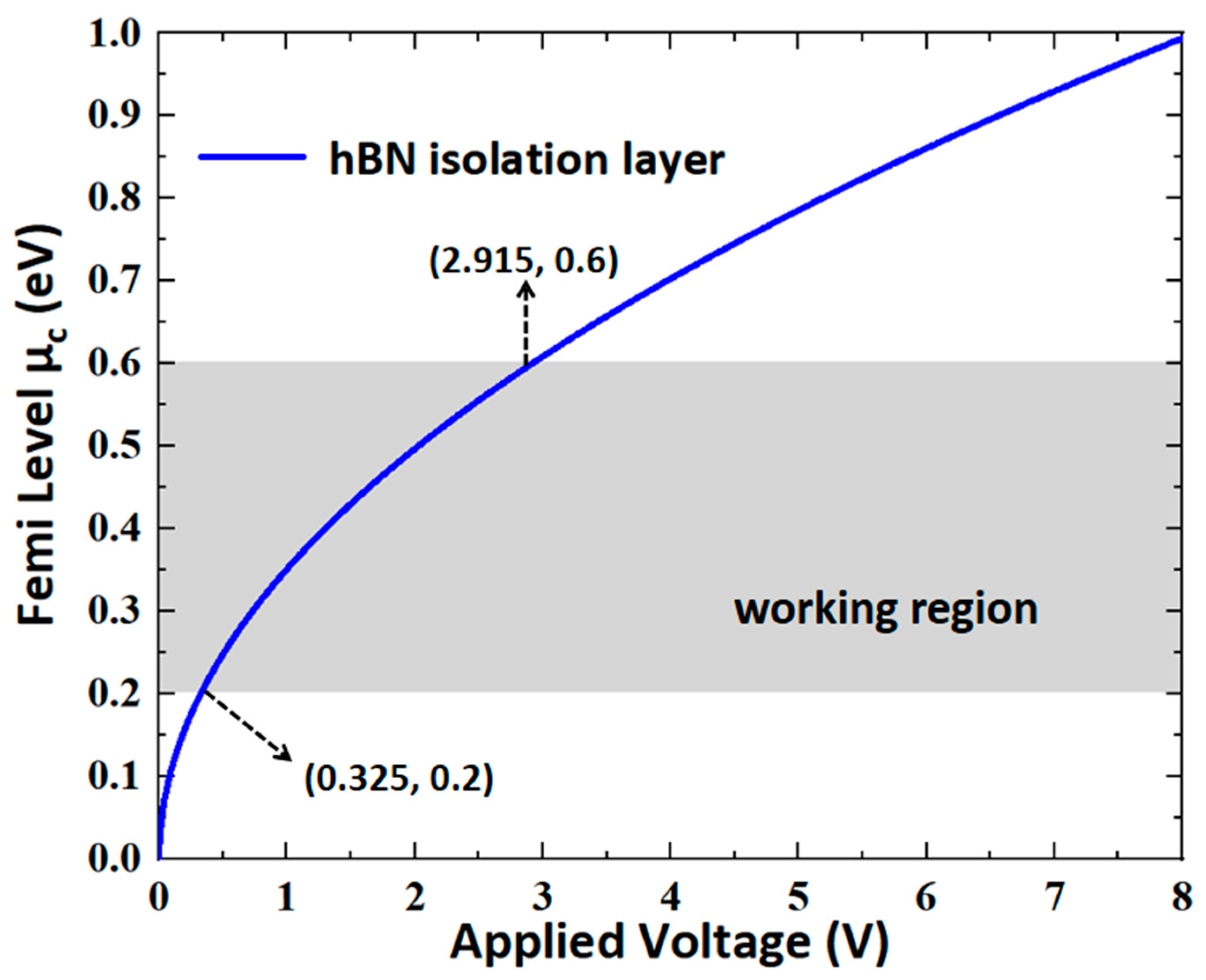
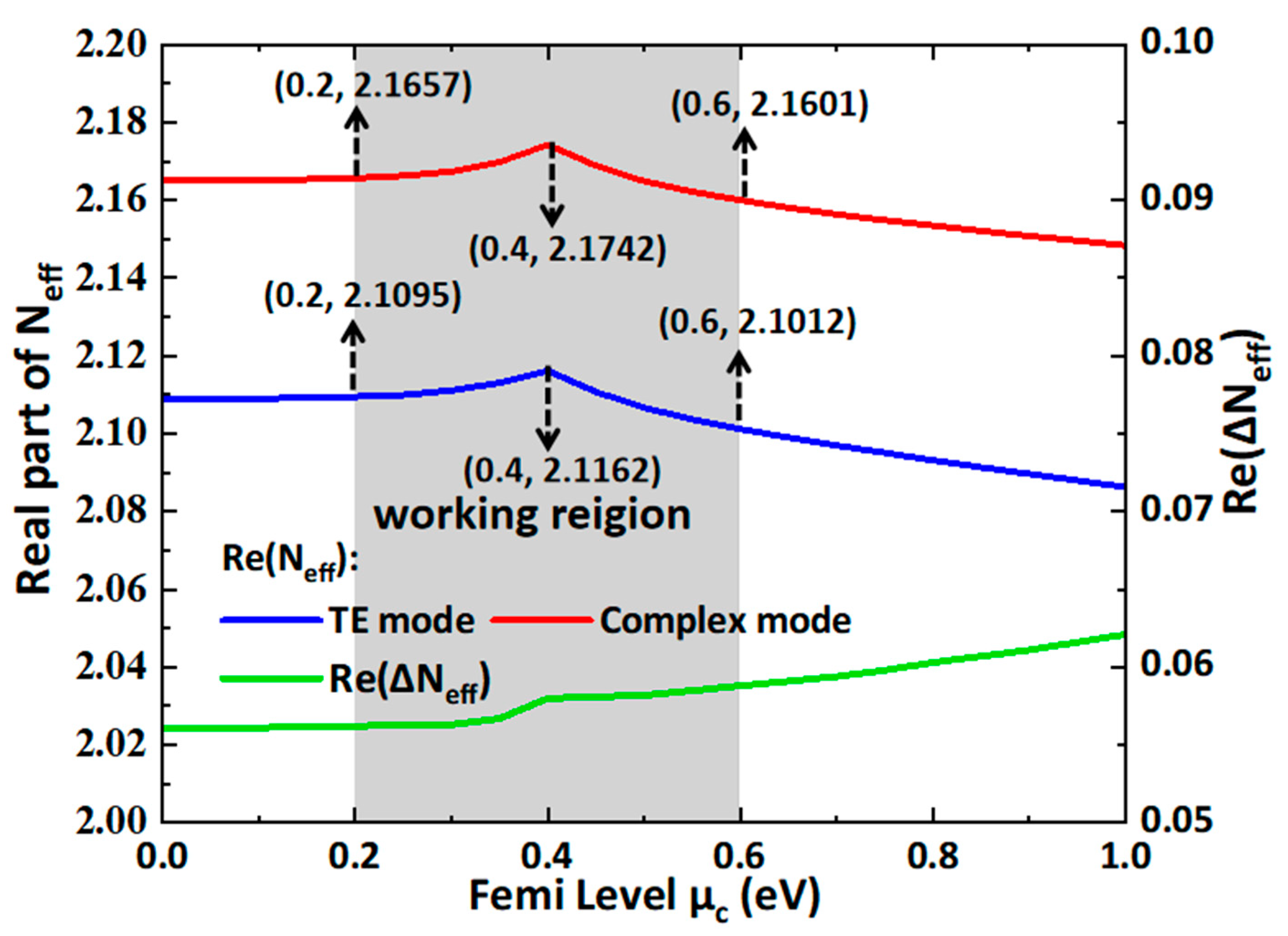
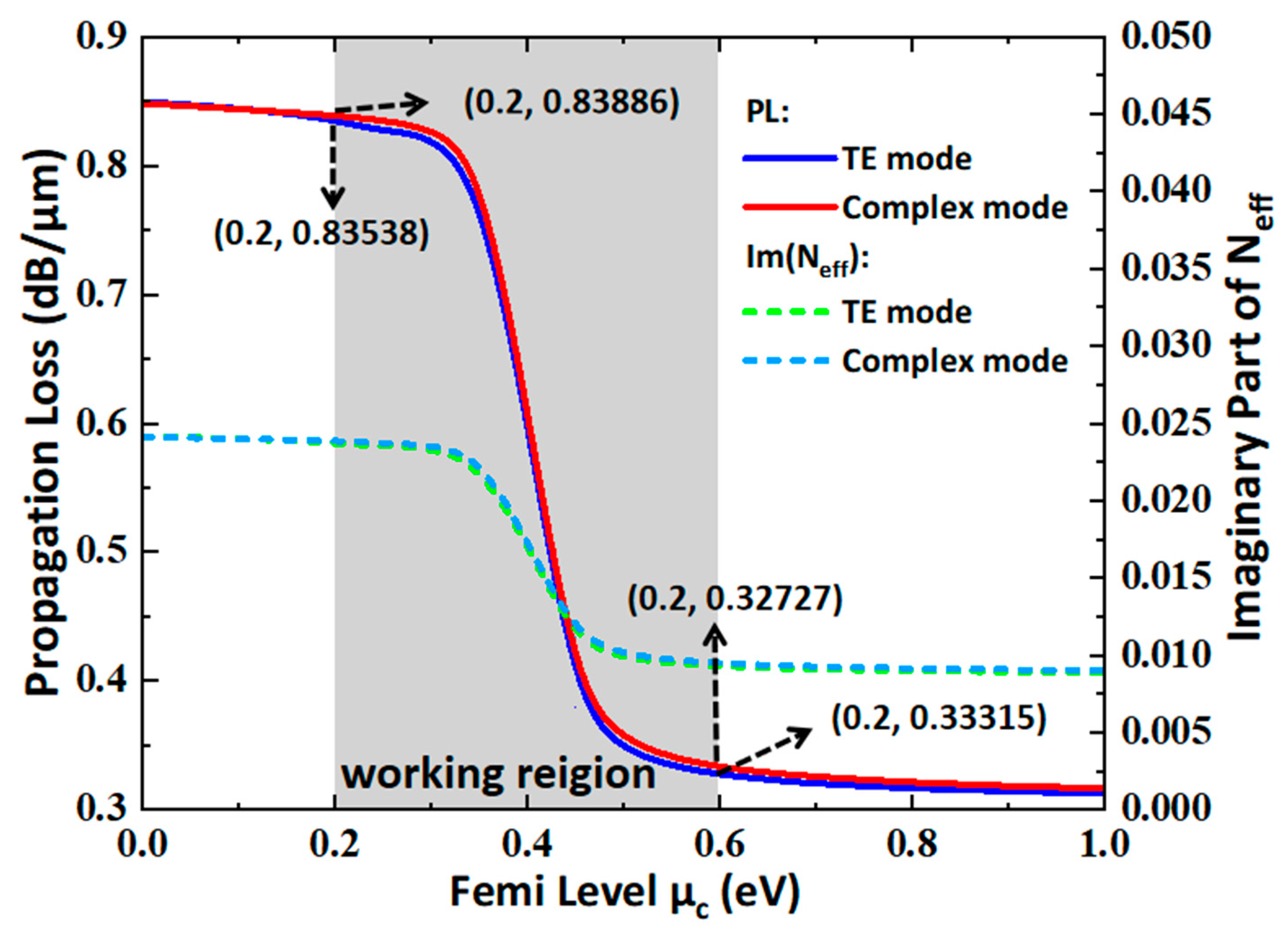
4.1. µc
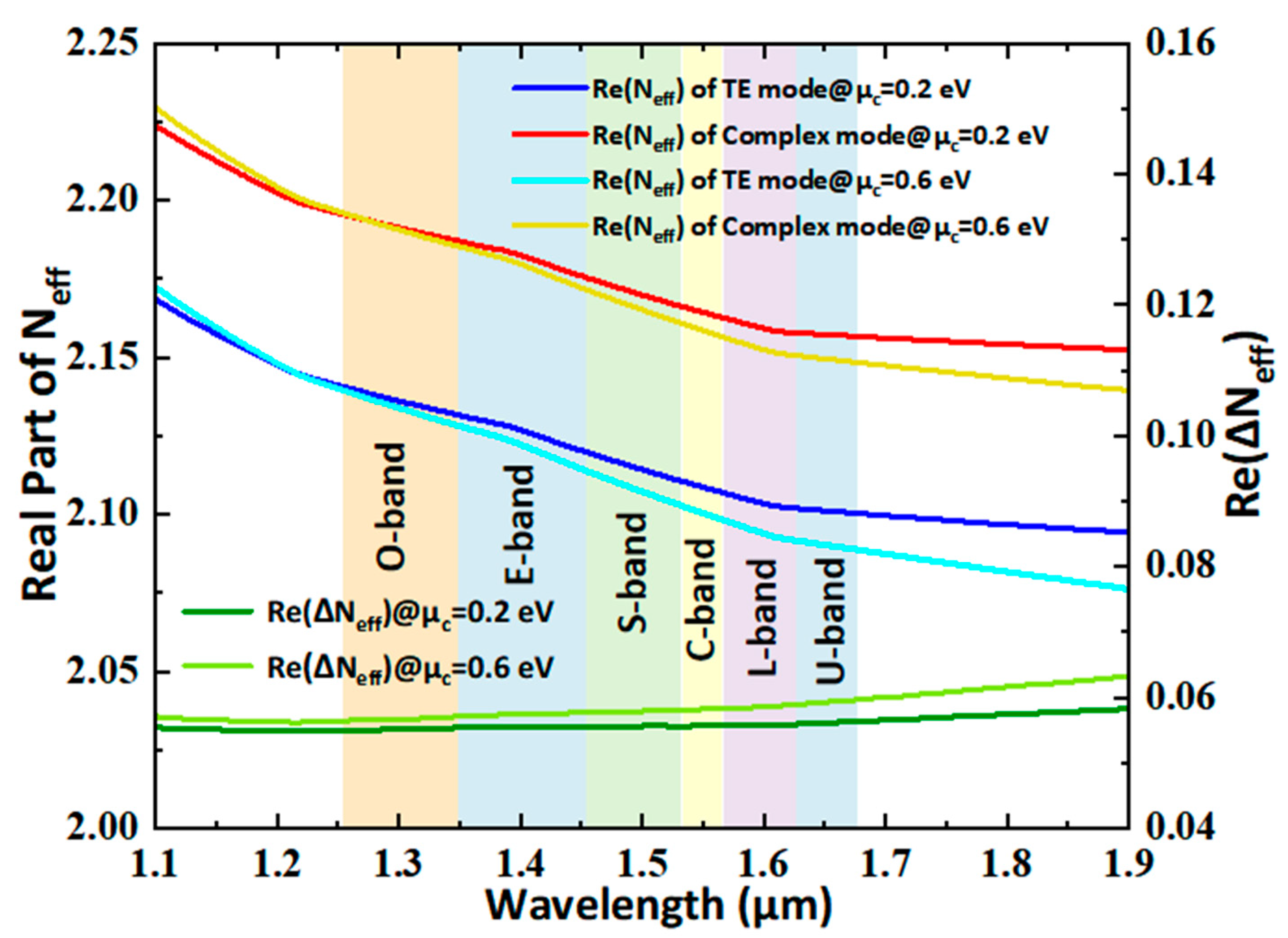
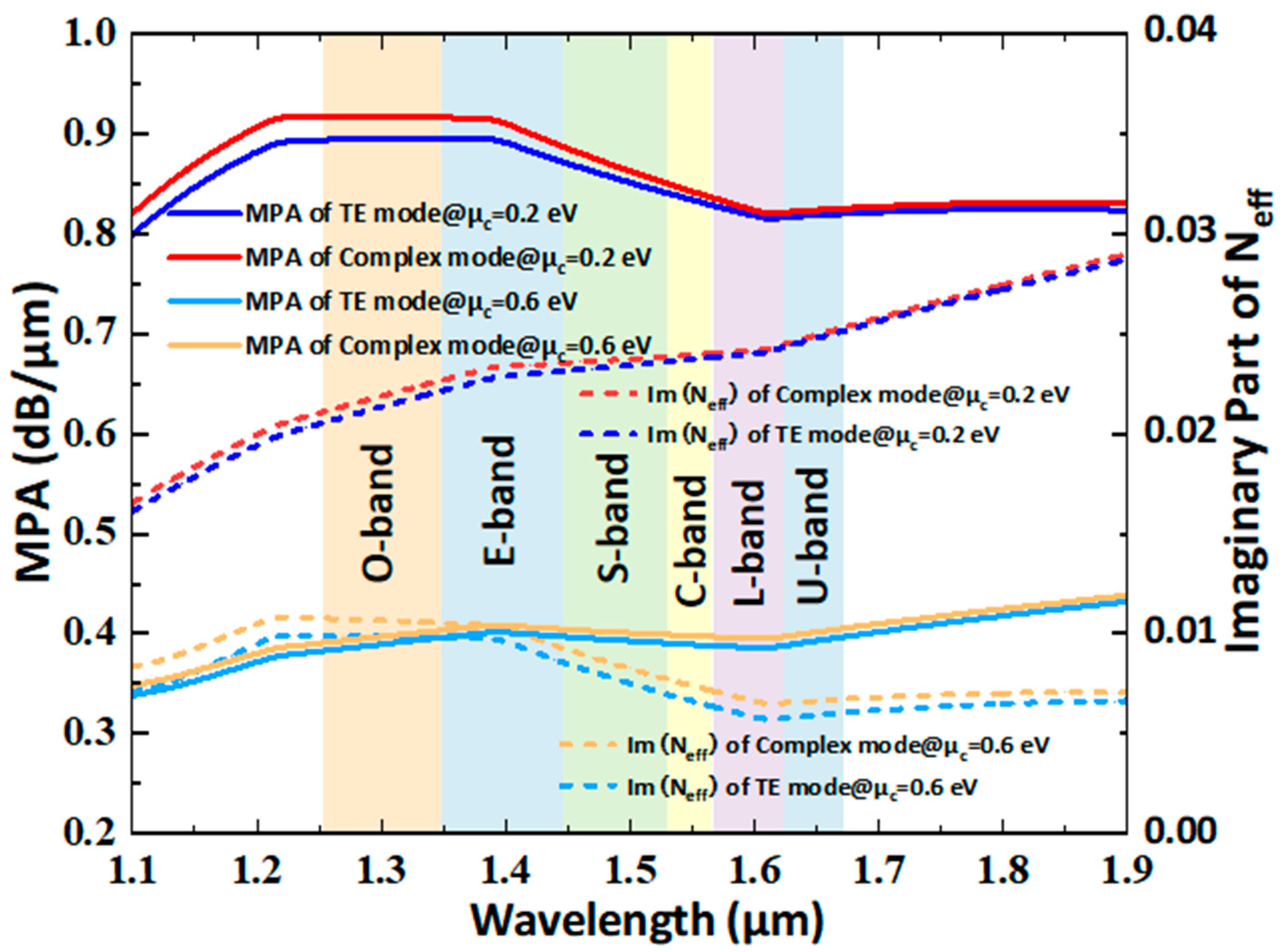
4.2. Optical Bandwidth
4.3. Frequency Response and Power Consumption
4.4. Discussion
5. Conclusions
Author Contributions
Funding
Institutional Review Board Statement
Informed Consent Statement
Data Availability Statement
Conflicts of Interest
References
- Bao, Q.; Loh, K.P. Graphene photonics, plasmonics, and broadband optoelectronic devices. ACS Nano 2012, 6, 3677–3694. [Google Scholar] [CrossRef] [PubMed]
- Mercante, A.J.; Eng, D.L.K.; Konkol, M.; Yao, P.; Shi, S.; Prather, D.W. Thin LiNbO3on insulator electro-optic modulator. Opt. Lett. 2016, 41, 867–869. [Google Scholar] [CrossRef] [PubMed]
- Pérez-Galacho, D.; Marris-Morini, D.; Stoffer, R.; Cassan, E.; Baudot, C.; Korthorst, T.; Boeuf, F.; Vivien, L. Simplified modeling and optimization of silicon modulators based on free-carrier plasma dispersion effect. Opt. Express 2016, 24, 26332–26337. [Google Scholar] [CrossRef]
- Jin-Kown, P.; Shinichi, T.; Mitsuru, T. InGaAsP Mach-Zehnder interferometer optical modulator monolithically integrated with InGaAs driver MOSFET on a III-V CMOS photonics platform. Opt. Express 2018, 26, 4842–4852. [Google Scholar]
- Qiu, F.; Yokoyama, S. Effificiently poled electro-optic polymer modulators. Opt. Express 2016, 24, 19020–19025. [Google Scholar] [CrossRef]
- Wang, X.; Jiang, M.; Sun, S.; Sun, J.; Yi, Y.; Chen, C.; Sun, X.; Wang, F.; Cui, Z.; Zhang, D. Demonstration of a high-speed electro-optic switch with passive-to-active integrated waveguide based on SU-8 material. RSC Adv. 2016, 6, 50166–50172. [Google Scholar] [CrossRef]
- Wang, F.; Zhang, Y.; Tian, C.; Girit, C.; Zettl, A.; Crommie, M.; Shen, Y. Gate-variable optical transitions in graphene. Science 2008, 320, 206–209. [Google Scholar] [CrossRef]
- Liu, M.; Yin, X.; Ulin-Avila, E.; Geng, B.S.; Thomas, Z.; Ju, L.; Wang, F.; Zhang, X. A graphene-based broadband optical modulator. Nature 2011, 474, 64–67. [Google Scholar] [CrossRef]
- Liu, M.; Yin, X.; Zhang, X. Double-layer graphene optical modulator. Nano Lett. 2012, 12, 1482–1485. [Google Scholar] [CrossRef]
- Gramotnev, D.K.; Bozhevolnyi, S.I. Plasmonics beyond the diffraction limit. Nat. Photonics 2010, 4, 83–91. [Google Scholar] [CrossRef]
- Rakib Hasan, K.B.M.; Noman Sarker, M.A.; Islam, M.A.; Alam, M.S. Coupling Characteristics of Surface Plasmons in Coupled Elliptical Nanowires. OSA Contin. 2018, 1, 1414–1428. [Google Scholar] [CrossRef]
- Huang, B.; Lu, W.; Li, X.; Wang, J.; Liu, Z. Waveguide-coupled hybrid plasmonic modulator based on graphene. Appl. Optics 2016, 55, 5598–5602. [Google Scholar] [CrossRef] [PubMed]
- Bao, Q.; Zhang, H.; Wang, B.; Ni, Z.; Lim, C.; Yi, X.; Wang, Y.; Tang, D.; Loh, K.P. Broadband graphene polarizer. Nat. Photonics 2011, 5, 411–415. [Google Scholar] [CrossRef]
- Okayama, H.; Onawa, Y.; Takahashi, H.; Shimura, D.; Sasaki, H. Polarization insensitive silicon waveguide wavelength filter using polarization rotator and mode conversion Bragg grating with resonator cavity. Jpn. J. Appl. Phys. 2020, 59, 128002. [Google Scholar] [CrossRef]
- Chang, L.; Lei, L.; Gong, Y.; Tan, M.; Yu, Y.; Li, Z. Polarization-independent directional coupler and polarization beam splitter based on asymmetric cross-slot waveguides. Appl. Optics 2018, 57, 678–683. [Google Scholar] [CrossRef]
- Zhong, H.; Zhang, Z.; Chen, B.; Xu, H.; Yu, D.; Huang, L.; Peng, L. Realization of low contact resistance close to theoretical limit in graphene transistors. Nano Res. 2015, 8, 1669–1679. [Google Scholar] [CrossRef]
- Veronis, G.; Fan, S. Modes of Subwavelength Plasmonic Slot Waveguides. J. Light. Technol. 2007, 25, 2511–2521. [Google Scholar] [CrossRef]
- Geim, A.K.; Novoselov, K.S. The rise of graphene. Nat. Mater. 2009, 6, 183–191. [Google Scholar] [CrossRef]
- Avouris, P.; Chen, Z.; Perebeinos, V. Carbon Based Electronics. Nat. Nanotechnol. 2007, 2, 605–615. [Google Scholar] [CrossRef]
- Ye, L.; Sui, K.; Zhang, Y.; Liu, Q. Broadband optical waveguide modulators based on strongly coupled hybrid graphene and metal nanoribbons for near-infrared applications. Nanoscale 2019, 11, 3229–3239. [Google Scholar] [CrossRef]
- Pasanen, P.; Voutilainen, M.; Helle, M.; Song, X.; Hakonen, P.J. Graphene for future electronics. Phys. Scr. 2012, T146, 014025. [Google Scholar] [CrossRef] [Green Version]
- Stauber, T.; Peres, N.M.R.; Geim, A.K. Optical conductivity of graphene in the visible region of the spectrum. Phys. Rev. B 2008, 78, 085432. [Google Scholar] [CrossRef]
- Sensale-Rodriguez, B.; Yan, R.; Kelly, M.M.; Fang, T.; Tahy, K.; Hwang, W.S.; Jena, D.; Liu, L.; Xing, H.G. Broadband graphene terahertz modulators enabled by intraband transitions. Nat. Commun. 2012, 3, 780–786. [Google Scholar] [CrossRef] [PubMed]
- Hwang, C.; Siegel, D.A.; Mo, S.K.; Regan, W.; Ismach, A.; Zhang, Y.; Zettl, A.; Lanzara, A. Fermi velocity engineering in graphene by substrate modification. Sci. Rep. 2012, 2, 590–593. [Google Scholar] [CrossRef]
- Hu, Y.; Xiao, X.; Xu, H.; Li, X.; Xu, K.; Li, Z.; Chu, T.; Yu, Y.; Yu, J. High-speed silicon modulator based on cascaded microring resonators. Opt. Express 2012, 20, 15079–15085. [Google Scholar] [CrossRef]
- Shiramin, L.A.; Thourhout, D.V. Graphene Modulators and Switches Integrated on Silicon and Silicon Nitride Waveguide. IEEE J. Sel. Top. Quantum Electron. 2017, 23, 94–100. [Google Scholar] [CrossRef]
- Koester, S.J.; Li, M. High-speed waveguide-coupled graphene-on-graphene optical modulators. Appl. Phys. Lett. 2012, 100, 171107. [Google Scholar] [CrossRef]
- Zheng, P.; Yang, H.; Fan, M.; Hu, G.; Zhang, R.; Yun, B.; Cui, Y. A Hybrid Plasmonic Modulator Based on Graphene on Channel Plasmonic Polariton Waveguide. Plasmonics 2018, 13, 2029–2035. [Google Scholar] [CrossRef]
- Yang, Z.; Lu, R.; Cai, S.; Wang, Y.; Liu, Y. A CMOS-compatible and polarization-insensitive graphene optical modulator. Opt. Commun. 2019, 450, 130–135. [Google Scholar] [CrossRef]
- Yang, Z.; Lu, R.; Wang, Y.; Cai, S.; Zhang, Y.; Wang, X.; Liu, Y. A fabrication-friendly graphene-based polarization insensitive optical modulator. Optik 2019, 182, 1093–1098. [Google Scholar] [CrossRef]
- Shirdel, M.; Mansouri-Birjandi, M.A. Broadband graphene modulator based on a plus-shaped plasmonic slot waveguide. Appl. Optics 2019, 58, 8174–8179. [Google Scholar] [CrossRef]
- Hu, X.; Wang, J. Design of graphene-based polarization-insensitive optical modulator. Nanophotonics 2018, 7, 651–658. [Google Scholar] [CrossRef]
- Xu, Y.; Li, F.; Kang, Z.; Huang, D.; Zhang, X.; Tam, H.Y.; Wai, P.K.A. Hybrid Graphene-Silicon Based Polarization-Insensitive Electro-Absorption Modulator with High-Modulation Efficiency and Ultra-Broad Bandwidth. Nanomaterials 2019, 9, 157. [Google Scholar] [CrossRef] [PubMed]
- Ye, S.; Liang, D.; Lu, R.; Shah, M.; Zou, X.; Yang, F.; Yuan, F.; Liu, Y. Polarization Independent Modulator by Partly Tilted Graphene Induced Electro-Absorption Effect. IEEE Photonics Technol. Lett. 2016, 29, 23–26. [Google Scholar] [CrossRef]
- Zou, X.; Zhang, Y.; Li, Z.; Yang, Y.; Zhang, S.; Zhang, Z.; Zhang, Y.; Liu, Y. Polarization-Insensitive Phase Modulators Based on an Embedded Silicon-Graphene-Silicon Waveguide. Appl. Sci. 2019, 9, 429. [Google Scholar] [CrossRef] [Green Version]


| Ref. | Bandwidth (nm) | Re(ΔNeff) | MD (dB/μm) | ΔMD (dB/μm) | f3dB (GHz) | Ebit (fJ/bit) |
|---|---|---|---|---|---|---|
| [29] | 1500–1600 | - | 0.06 | 0 | 13.4 | - |
| [30] | 1500–1600 | - | 0.08 | 0 | 80 | - |
| [31] | 1200–1600 | - | mode A: 1.05, mode B: 1.13, mode C: 0.52 | Min: 0.08 Max: 0.61 | 95 | 138.8 |
| [32] | 1530–1565 | 4.7 × 10⁻³ | TM mode: ~0.2975, TE mode: ~0.2895 | ~8 × 10⁻³ | 30.2 | 2980 |
| [33] | 1367–1771 | ~0.5 | TM mode: 1.113, TE mode: 1.119 | ~6 × 10⁻³ | 6.1 | 7800 |
| [34] | 1450–1650 | ~0.1 | TM mode: 1.392, TE mode: 1.347 | 0.045 | ~100 | - |
| [35] | 1300–1800 | 1.2 × 10⁻³ | - | - | 135.6 | - |
| This work | 1100–1900 | 5 × 10⁻² | TE mode: 0.511, complex mode: 0.502 | 0.009 | 127 | 72 |
Publisher’s Note: MDPI stays neutral with regard to jurisdictional claims in published maps and institutional affiliations. |
© 2022 by the authors. Licensee MDPI, Basel, Switzerland. This article is an open access article distributed under the terms and conditions of the Creative Commons Attribution (CC BY) license (https://creativecommons.org/licenses/by/4.0/).
Share and Cite
Liu, S.; Wang, M.; Liu, T.; Xu, Y.; Yue, J.; Yi, Y.; Sun, X.; Zhang, D. Polarization-Insensitive Graphene Modulator Based on Hybrid Plasmonic Waveguide. Photonics 2022, 9, 609. https://doi.org/10.3390/photonics9090609
Liu S, Wang M, Liu T, Xu Y, Yue J, Yi Y, Sun X, Zhang D. Polarization-Insensitive Graphene Modulator Based on Hybrid Plasmonic Waveguide. Photonics. 2022; 9(9):609. https://doi.org/10.3390/photonics9090609
Chicago/Turabian StyleLiu, Songyue, Manzhuo Wang, Tingyu Liu, Yan Xu, Jianbo Yue, Yunji Yi, Xiaoqiang Sun, and Daming Zhang. 2022. "Polarization-Insensitive Graphene Modulator Based on Hybrid Plasmonic Waveguide" Photonics 9, no. 9: 609. https://doi.org/10.3390/photonics9090609