Article

Flat Optical Frequency Comb Generation Based on Monolithic Integrated LNOI Intensity and Phase Modulator

1
State Key Laboratory of Electronic Thin Films and Integrated Devices, School of Optoelectronic Science and Engineering, University of Electronic Science and Technology of China, Chengdu 610054, China
2
Wuhan National Laboratory for Optoelectronics, Huazhong University of Science and Technology, Wuhan 430074, China
3
Beijing Institute of Radio Measurement, Beijing 100854, China
*
Author to whom correspondence should be addressed.
Photonics 2022, 9(7), 495; https://doi.org/10.3390/photonics9070495
Submission received: 18 June 2022 / Revised: 12 July 2022 / Accepted: 13 July 2022 / Published: 14 July 2022

Abstract

:
A flat optical frequency comb (OFC) is generated by using a monolithic integrated electro-optic intensity and phase modulator fabricated on lithium niobite on insulator (LNOI) platform. The LNOI-based modulation chip consists of a push–pull Mach–Zehnder modulator (MZM) and a U-shaped phase modulator (PM) connected by a curved optical waveguide. Microwave and optical packaging are implemented for the modulation chip, where the input and output pigtails of the packaged modulation device are polarization-maintaining fibers, with a core diameter of 6.5 μm. The packaged LNOI-based modulation device is featured by a fiber-to-fiber insertion loss as low as 6.97 dB. The half-wave voltages of the MZM and the PM are measured to be 3.6 V and 3.4 V at 5 GHz, respectively. By using the modulation device, an OFC with a tooth spacing of 5 GHz is generated, and the 13 comb teeth in the generated OFC are with a power flatness of 2.4 dB. The measured results of this device indicate that the tooth spacing of the generated OFC can be extended to tens of gigahertz by using a microwave source with a higher output frequency. In addition, the number of the comb teeth can be enhanced beyond 20 by increasing the power of the radio-frequency signal applied to the PM or by further reducing the half-wave voltage of the PM.

1. Introduction

Optical frequency comb (OFC) is a powerful tool for providing uniformly distributed optical carriers, which has been widely used in applications such as metrology, spectroscopy, optical imaging, optical communications, and microwave photonics [1,2,3,4,5,6]. The common methods of generating an OFC include mode-locked lasers [7], nonlinear optical micro-resonators [8], and electro-optic modulation [9,10,11,12,13]. Thereinto, the OFC generated by electro-optic modulation (i.e., electro-optic frequency comb) has the advantages of well-definable frequency interval and freely tunable center wavelength, and is recognized as the most attractive solution to provide multiple optical carriers in the dense wavelength division multiplexing (DWDM) systems.
Thereinto, the OFC generated by electro-optic modulation (i.e., electro-optic frequency comb) has the advantages of a well-definable frequency interval and freely tunable center wavelength, and it is recognized as the most attractive solution for providing multiple optical carriers in the dense wavelength multiplexing (DWDM) systems.
An electro-optic frequency comb can be generated by using a single electro-optic modulator, such as a push–pull Mach–Zehnder modulator (MZM), a dual-drive MZM, an in-phase and quadrature (IQ) modulator, a polarization modulator, a phase modulator (PM), and a silicon-based micro-ring modulator [9,10,11,12]. However, the power flatness of the OFCs generated by using a single electro-optic modulator is generally poor. This problem can be effectively solved by cascading an intensity modulator with a single PM or multiple PMs [13]. Nevertheless, the system architecture, based on discrete commercial modulation devices, is bulky and costly. Additionally, the optical power per comb tooth is generally weak due to the high insertion loss introduced by the multiple inefficient fiber-to-chip and chip-to-fiber coupling [14]. Therefore, cascading multiple modulators on a single chip with a low insertion loss is critically important to enhance the performance of the electro-optic frequency comb.
Silicon-on-insulator (SOI) and indium phosphide (InP) are workable platforms for integrating multiple modulators on a single chip, both of which have already been utilized to realize chip-scale electro-optic frequency comb generation [15,16]. In addition, lithium niobate on insulator (LNOI), with a strong electro-optic effect, a large modulation bandwidth, and a broad optical transparent window, is recognized as a promising candidate for realizing power-efficient chip-scale electro-optic frequency comb generation with a large tooth spacing tuning range and a high output power. Recently, flat OFC generation has been demonstrated by using a monolithic integrated LNOI intensity and phase modulator [17]. However, the LNOI-based modulation chip used in the experimental demonstration has not been packaged. In the experiment of electro-optic frequency comb generation, the radio-frequency (RF) signals are applied to the intensity and phase modulators through RF probes. In addition, the light is coupled into and out of the chip through grating couplers, which inevitably introduces a large insertion loss.
In this paper, a flat OFC is generated by using a packaged monolithic integrated LNOI intensity and a phase modulator. The packaged modulation device is featured by a fiber-to-fiber insertion loss as low as 6.97 dB. By using this device, an OFC with 13 comb teeth, a tooth spacing of 5 GHz, and a power flatness of 2.4 dB is generated.

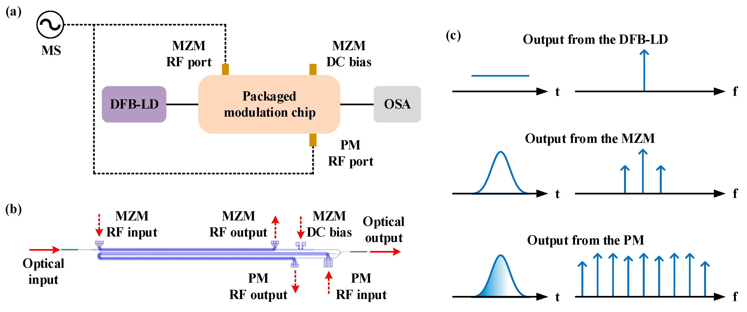
2. Operation Principle

Figure 1 shows the schematic diagram of the OFC generation based on a packaged monolithic integrated LNOI intensity and phase modulator. Thereinto, Figure 1a shows the experimental setup of the OFC generation. Figure 1b exhibits the layout of the LNOI-based modulation chip. Figure 1c presents the time-domain and the frequency-domain evolution of the light wave in the modulation chip. The LNOI modulation chip involves a push–pull MZM with an 8.5-mm-long, straight ground-signal-ground (GSG) coplanar waveguide electrode and a U-shaped PM with a 24.5-mm-long curved coplanar waveguide electrode, where the MZM and the PM are connected by a curved optical waveguide as shown in Figure 1b. The bias phase shift of the MZM is realized by applying a direct-current (DC) voltage to the heater on the LNOI optical waveguide. In addition, spot-size converters are fabricated at the input and the output ends of the LNOI modulation chip to achieve high-efficiency optical coupling to the polarization, maintaining fiber (PMF) with a core diameter of 6.5 μm [18]. The OFC is generated by injecting a continuous-wave (CW) light from a distributed feedback laser diode (DFB-LD) into the packaged LNOI modulation device, as shown in Figure 1a. In the modulation device, the CW light is, firstly, carved into a chirp-free pulse train with a repetition rate of f R F by applying a single-tone RF signal at f R F to the push–pull MZM as shown in Figure 1c. Then, the optical pulse train from the MZM is injected into the PM, where it is modulated by another high-power single-tone RF signal at f R F . The RF signal applied to the PM is synchronized with that applied to the MZM, and its phase is finely adjusted to guarantee that the peak or the valley of the single-tone RF signal aligns with each optical pulse in the PM. Therefore, a large chirp is introduced into the optical pulse train, which greatly enhances the number of the generated comb teeth. In addition, the DC bias voltage and the modulation index of the MZM are finely adjusted to optimize the flatness of the generated OFC.
Mathematically, the optical field from the MZM can be calculated as
E MZM ( t ) = α E 0 exp ( j ω 0 t ) cos ( φ D C 2 + m M Z M 2 cos ( ω R F t ) ) = α E 0 exp ( j ω 0 t ) [ n = cos ( φ D C 2 + n 2 π ) J n ( m M Z M 2 ) exp ( j n ω R F t ) ]
where E 0 and ω 0 are the amplitude and the center angular frequency of the CW light from the DFB-LD. α is the amplitude loss introduced by the fiber-to-chip coupling and the propagation in the MZM. m M Z M = π V R F 1 / V π _ M Z M and φ D C = π V b i a s / V π _ D C are the modulation index and the DC bias voltage-induced phase shift of the MZM, respectively. Thereinto, V π _ M Z M and V π _ D C are the RF half-wave voltage and the DC half-wave voltage of the MZM, respectively. V b i a s and V R F 1 are the voltage amplitudes of the DC bias and the single-tone RF signal applied to the MZM, respectively. ω R F is the angular frequency of the single-tone RF signal applied to the MZM. J n ( ) is the nth-order Bessel function of the first kind.
The optical field from the PM can be calculated as
E P M ( t ) = β E M Z M ( t ) exp ( j m P M cos ( ω R F t ) ) = α β E 0 exp ( j ω 0 t ) [ N = n = cos ( φ D C 2 + n 2 π ) J n ( m M Z M 2 ) j N n J N n ( m P M ) exp ( j ( N n ) π ) exp ( j N ω R F t ) ]
where β is the amplitude loss introduced by the propagation in the PM and the chip-to-fiber coupling. m P M = π V R F 2 / V π _ P M is the modulation index of the PM. Thereinto, V R F 2 and V π _ P M are the voltage amplitude of the single-tone RF signal applied to the PM and the half-wave voltage of the PM, respectively. It can be seen, from Equation (2), that the output optical field is an OFC with an angular frequency interval of ω R F , where the amplitude of each comb tooth is dependent on the optical power from the DFB-LD, the fiber-to-fiber insertion loss of the packaged LNOI modulation device, the DC bias phase shift of the MZM, and the modulation indices of MZM and the PM. Therefore, through finely tuning the DC bias voltage and the modulation index of the MZM, a flat OFC can be generated.

3. Results and Discussion

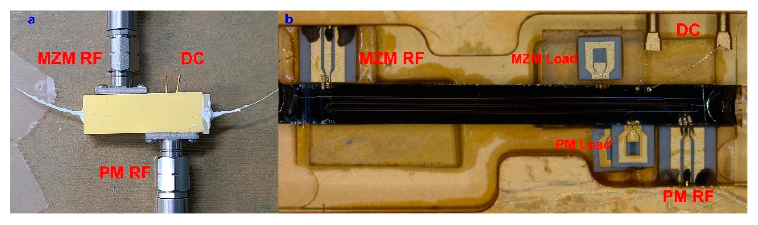
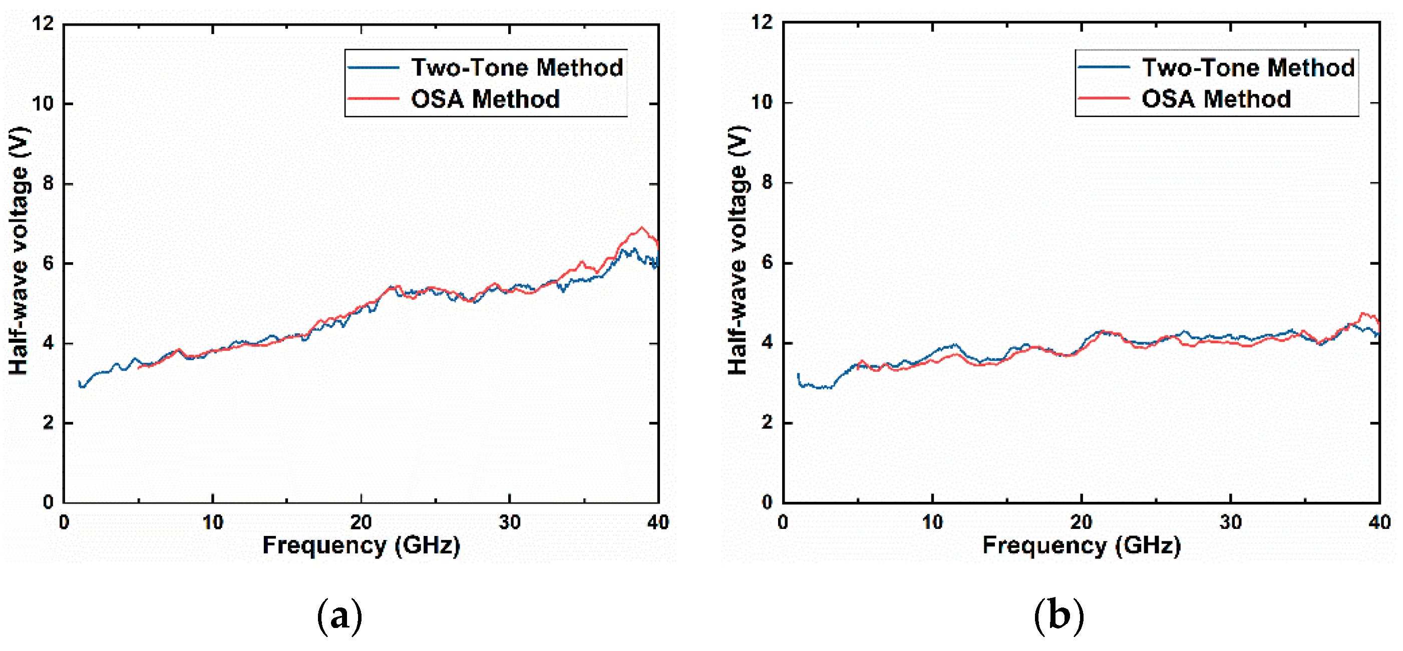
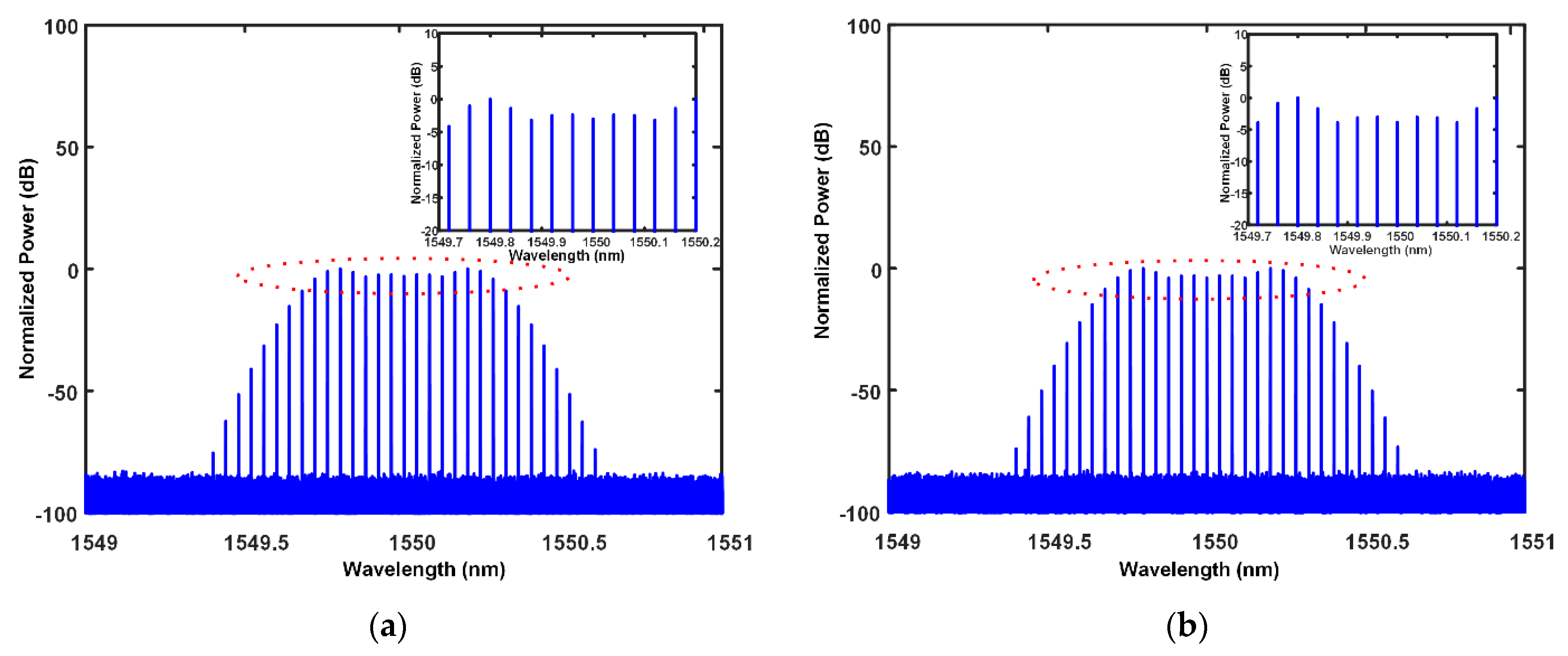
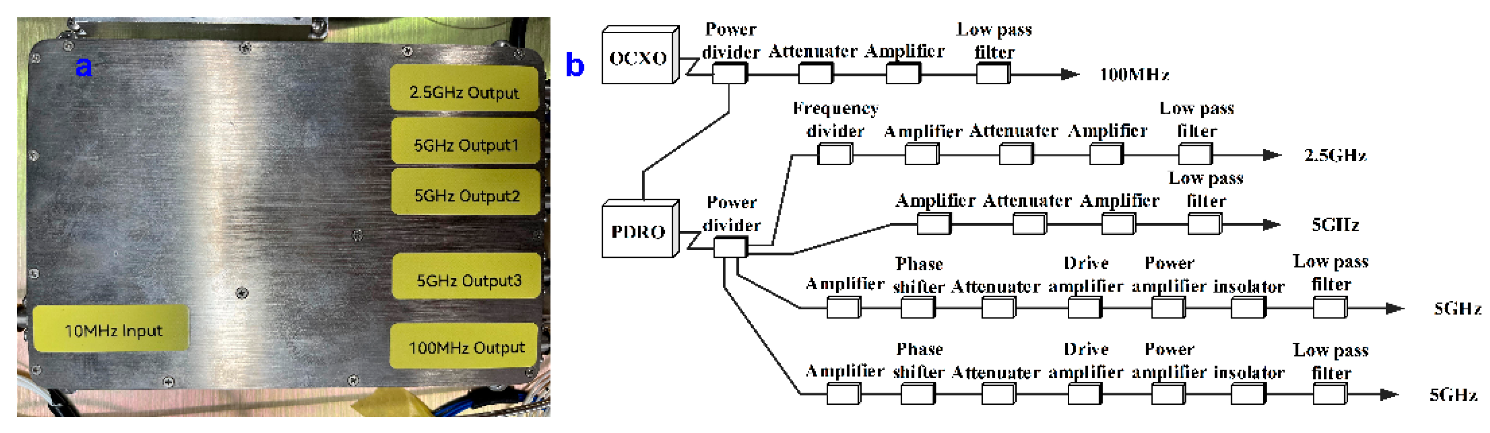
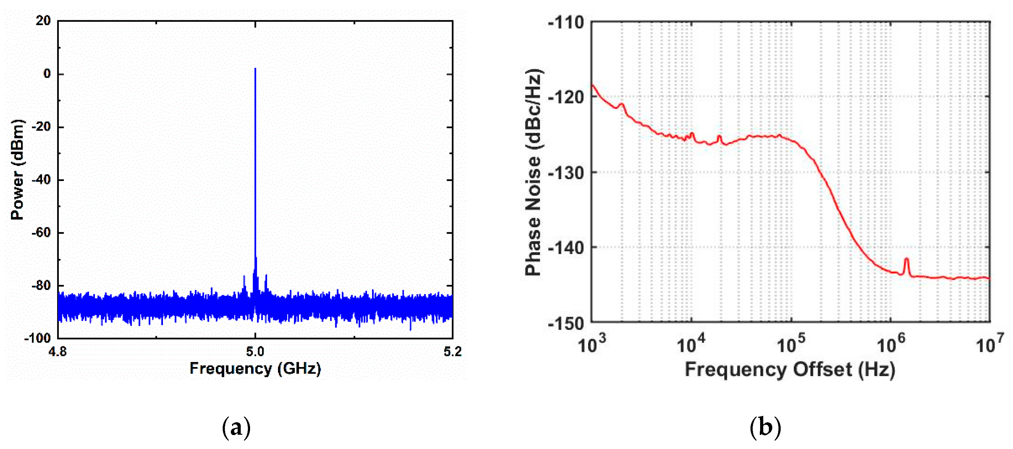
3.1. Device Characterization

Figure 2 shows the photograph of the packaged LNOI modulation device. Thereinto, Figure 2a is the exterior appearance of the packaged device, and Figure 2b is the internal layout of the device. The internal layout of the device can refer to that in Figure 1b. The LNOI modulation chip is fabricated on a commercial LNOI wafer (NANOLN), which includes 500-μm-thick silicon substrate, 4.7-μm-thick buried oxide, and 500-nm-thick LN. The LNOI waveguide is with a ridge waveguide structure, which is fabricated by using electron beam lithography (EBL). The inclination angle of the side wall is 66°. The etching depth and the width of the LNOI ridge waveguide are 260 nm and 1.5 μm, respectively. In addition, the thickness of the Au electrode is 1200 nm. A 2-μm-thick SiO2 layer covers the electrode as the upper cladding. The length and the width of the device are 38 mm and 8.5 mm, respectively. For the RF packaging, the LNOI modulation chip, with a length of 16 mm and a width of 1.4 mm, is placed into a metal tube shell, where two RF coaxial connectors fixed on the side wall of the shell are used to load the RF signals into the shell. Two ceramic transmission lines are employed to apply the RF signals to the MZM and the PM, which are connected to the two RF coaxial connectors and the electrodes of the modulation chip via gold wires and gold tapes. At the end of the MZM and the PM electrodes, there are matching resistors to reduce the RF signal reflection. For the optical packaging, customized single-channel fiber arrays (FAs) are employed to align the PMFs with the spot-size converters at the input and the output ends of the LNOI modulation chip, and they are fixed by using ultraviolet curing adhesive.
Through biasing the MZM in the packaged device at its maximum transmission point, the fiber-to-fiber insertion loss of the device is measured to be 6.97 dB, where the fiber-chip coupling loss is about 2.1 dB/facet, and the propagation loss in the waveguide is 0.8 dB/cm. This value is smaller than that introduced by cascading a LN-based MZM with a LN-based PM, which is favorable for enhancing the power of the generated OFC. The half-wave voltages of the MZM and the PM, at different modulation frequencies, are independently measured by using the optical spectrum analysis (OSA) method [19] and the two-tone modulation method [20]. In the measurement, a DFB-LD, centered at 1555.6 nm and with an output power of 12.7 dBm, is employed to generate the CW optical carrier. The DC bias voltage of the MZM is finely adjusted by using a high-accuracy power supply (Keithley 2200-30-5) to guarantee that the MZM works at its quadrature point. Figure 3a,b present the half-wave voltages of the PM and the MZM, respectively, in which the red lines are measured by using an optical spectrum analyzer (YOKOGAWA AQ6370C), and the blue lines are measured by using a four-port vector network analyzer (Keysight N5225A). The measurement results indicate that the half-wave voltages obtained by using the two methods fit in with each other. Hence, the measurement results in Figure 3 are credible, so they are used to optimize the OFC generation.

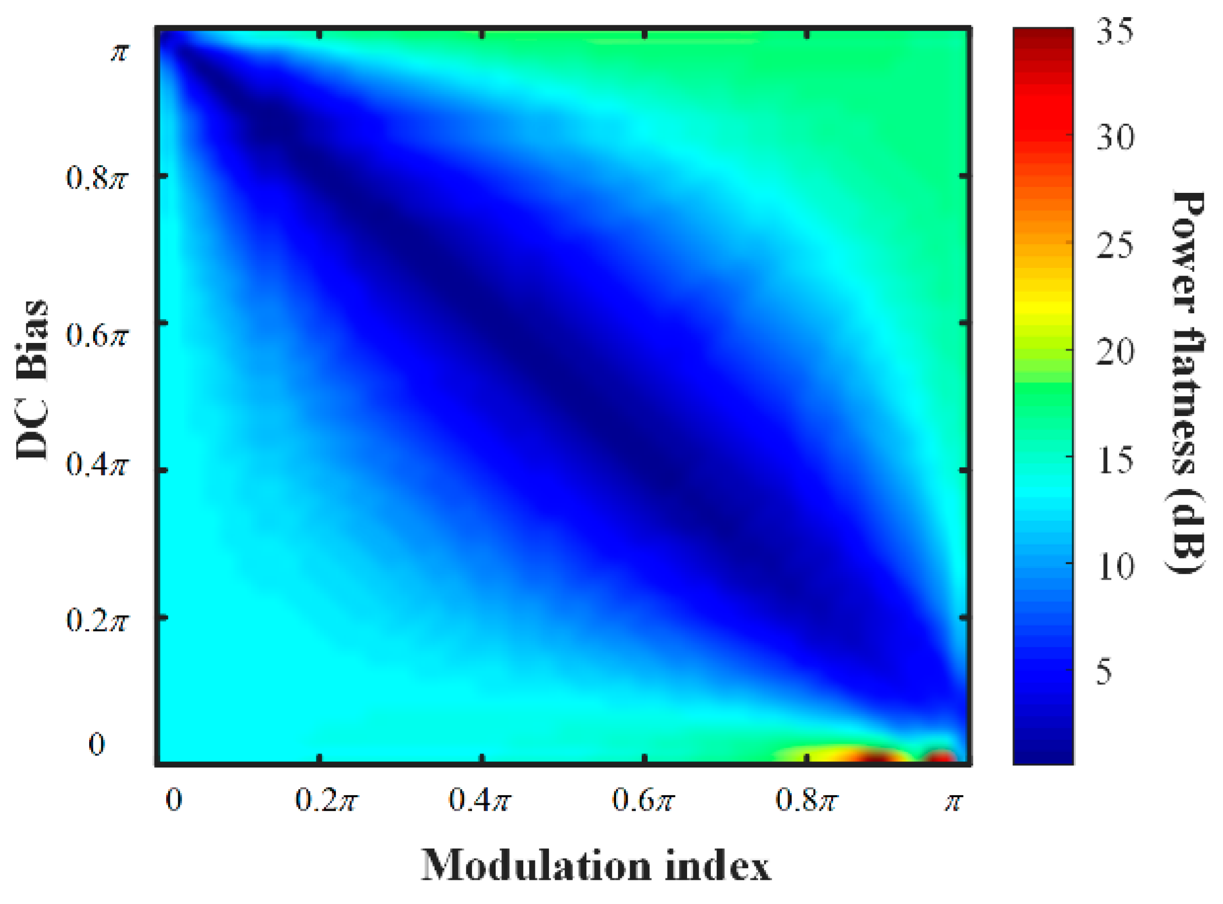
3.2. Simulation Results

Numerical simulation is implemented to optimize the OFC generation, based on cascaded MZM and PM by using the Fortran software. The simulation is based on the transmission equations of the MZM and the PM. In the simulation, the microwave signals applied to the two modulators are synchronized with each other. In addition, the spectrum of the OFC is calculated by implementing fast Fourier transform (FFT) of the temporal optical field. Figure 4 shows the power flatness of the generated OFC under a different modulation index and DC bias of the MZM. It can be seen, from Figure 4, that the combinations of modulation index and DC bias, in the dark blue area, are beneficial for enhancing the power flatness of the OFC. Figure 5 exhibits the simulated spectra of the generated OFCs. Thereinto, in Figure 5a, the MZM is biased at 0.6 π and with a modulation index of 0.4 π . In Figure 5b, the MZM is biased at 0.5 π (i.e., its quadrature point) and with a modulation index of 0.5 π . These two conditions are in the dark blue area of Figure 4. It can be seen, from the insets of Figure 5, that the power flatness of the OFC is smaller than 5 dB.

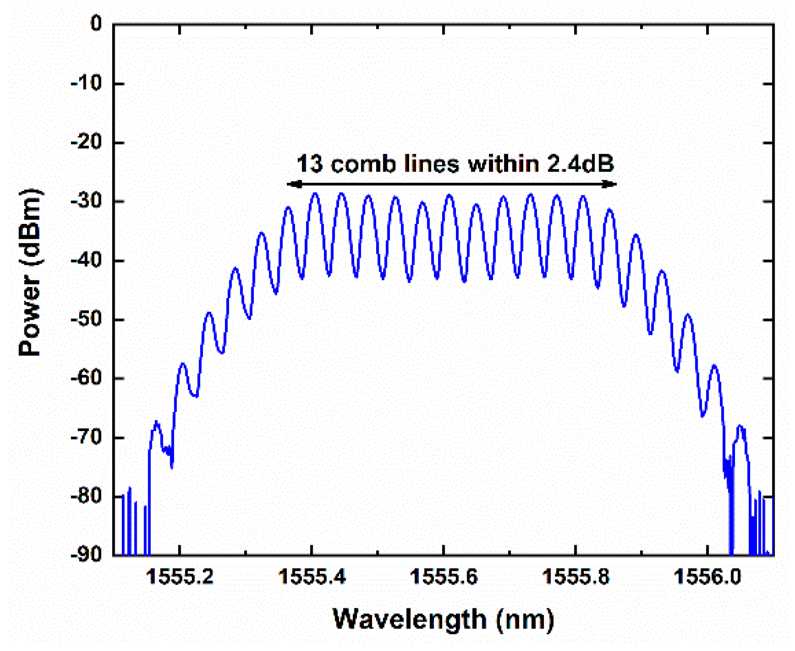
3.3. Experimental Results

In the OFC generation experiment, a DFB-LD, centered at 1555.6 nm and with an output power of 12.7 dBm, is employed to generate the CW optical carrier, whose pigtail is a polarization-maintaining fiber with a core diameter of 6.5 μm. The RF signals applied to the MZM and the PM are generated by a home-made multi-port microwave source as shown in Figure 6. Thereinto, Figure 6a exhibits the exterior appearance of the microwave source, and Figure 6b presents the internal architecture of the microwave source. The single-tone RF signals from the microwave source at 5 GHz are synchronized by using a single 100-MHz oven-controlled crystal oscillator (OCXO) integrated in the microwave source, which guarantees the stability of the generated OFC. The output RF signal power and the phase difference between the single-tone RF signals can be finely tuned via the electrically-controlled variable attenuator (VOA) and RF phase shifter integrated in the microwave source, which can help to optimize the power flatness of the generated OFC.
Figure 7a,b exhibit the spectrum and the phase noise of the output RF signal measured by using an electrical spectrum analyzer (R&S, FSU50) and a phase noise analyzer (R&S, FSWP50), respectively. The measurement results indicate that the output RF signal at 5 GHz is clear and with an excellent phase noise performance (the corresponding time jitter, integrated from the 1 kHz to 10 MHz offset frequency, is 13.8 fs), which guarantees the quality of the generated OFC. To generate a flat OFC, the MZM is biased at its quadrature point, and the phase difference between the two RF signals applied to the MZM and the PM is finely tuned to guarantee that the peak or the valley of the single-tone RF signal aligns with each optical pulse in the PM. It can be seen, from Figure 3, that the half-wave voltages of the MZM and the PM are 3.6 V and 3.4 V at 5 GHz, respectively. Therefore, the RF power applied to the MZM and the PM are set to be 11.24 dBm and 24.96 dBm in the experiment, respectively, to optimize the power flatness of the generated OFC. On this condition, the total power consumption of the LNOI modulation device is about 380 mW, which includes the RF power applied to the modulation device and the DC bias power consumption of about 50 mW in the MZM.
Figure 8 shows the measured spectrum of the generated OFC after 20-dB optical attenuation. It can be seen that 13 comb teeth with a power flatness of 2.4 dB are obtained. The power flatness is mainly limited by the relatively large power tuning step of the microwave source, i.e., 0.5 dB. If a microwave source with a higher power tuning accuracy is used, the power flatness of the OFC can be further improved. It should be noted that the number of the comb teeth can be further increased through applying a large RF signal power to the PM, which will not introduce an extra loss into the optical link. In fact, the maximum output power of the microwave source is up to 33 dBm. Nevertheless, this high power is not used in the experiment since the matching resistor at the end of the PM electrode, in the present packaged device, cannot handle such a high power. The modulation device with a higher RF signal power handling capacity is in fabrication, which is expected to generate more than 20 comb teeth with an excellent power flatness. Finally, it should be pointed out that the packaged LNOI modulation device can work in the frequency range up to 40 GHz as shown in Figure 3. Hence, it can be used to generate OFCs with comb spacing up to 40 GHz if the corresponding microwave source is employed.

4. Conclusions

In summary, we have proposed and demonstrated flat OFC generation based on a packaged, monolithic integrated LNOI intensity and phase modulator. The LNOI modulation chip involves a push–pull MZM and a U-shaped PM connected by a curved optical waveguide. After packaging, the fiber-to-fiber insertion loss of the modulation device was measured to be as low as 6.97 dB. In addition, the half-wave voltages of the MZM and the PM, in the packaged modulation device, were measured to be 3.6 V and 3.4 V at 5 GHz, respectively. This low insertion loss is beneficial for enhancing the power of the OFC generated by using a monolithic integrated LNOI intensity and phase modulator. In the OFC generation experiment, 13 comb teeth, with a power flatness of 2.4 dB and a tooth spacing of 5 GHz, were obtained. The number of comb teeth and the tooth spacing can be further enhanced since the LNOI-based electro-optic modulator is featured with a large modulation bandwidth and a low half-wave voltage. These results indicate that LNOI is an excellent platform for achieving power-efficient, chip-scale, electro-optic frequency comb generation. The future work should be focused on further decreasing the half-wave voltage of the PM and the fiber-chip coupling loss. In addition, a well-packaged matching resistor with a high-power handling capacity should be used at the end of the PM to help increase the modulation index of the PM. Under this condition, flat OFCs with increased comb number can be generated.

Author Contributions

Conceptualization, Z.Z. and C.Z.; methodology, Y.Z. (Yujia Zhang), X.W. and Z.L.; software, Z.L.; validation, Y.Z. (Yali Zhang) and S.Z.; formal analysis, Y.Z. (Yujia Zhang); investigation, Y.Z. (Yujia Zhang), X.W., Z.L., W.L. and Y.L. (Yanjia Lyu); resources, H.L.; data curation, Y.Z. (Yujia Zhang); writing—original draft preparation, Y.Z. (Yujia Zhang); writing—review and editing, Z.Z.; visualization, Y.Z. (Yujia Zhang); supervision, Y.L. (Yong Liu) and J.X.; project administration, H.L.; funding acquisition, H.L. and Y.L. (Yong Liu). All authors have read and agreed to the published version of the manuscript.

Funding

This research was funded by the National Key Research and Development Program of China (2019YFB2203800), the National Natural Science Foundation of China (61927821), and the Fundamental Research Funds for the Central Universities (ZYGX2020ZB012).

Institutional Review Board Statement

Not applicable.

Informed Consent Statement

Not applicable.

Data Availability Statement

Data underlying the results presented in this paper are not publicly available at this time but may be obtained from the authors upon reasonable request.

Conflicts of Interest

The authors declare no conflict of interest.

References

  1. Schiller, S. Spectrometry with frequency combs. Opt. Lett. 2002, 27, 766–768. [Google Scholar] [CrossRef] [PubMed] [Green Version]
  2. Parriaux, A.; Hammani, K.; Millot, G. Two-micron all-fibered dual-comb spectrometer based on electro-optic modulators and wavelength conversion. Commun. Phys. 2018, 1, 17. [Google Scholar] [CrossRef]
  3. Kang, J.; Feng, P.; Li, B.; Zhang, C.; Wei, X.; Lam, E.Y.; Tsia, K.K.; Wong, K.K.Y. Video-rate centimeter-range optical coherence tomography based on dual optical frequency combs by electro-optic modulators. Opt. Express 2018, 26, 24928–24939. [Google Scholar] [PubMed] [Green Version]
  4. Murphy, M.T.; Udem, T.H.; Holzwarth, R.; Sizmann, A.; Pasquini, L.; Araujo-Hauck, C.; Dekker, H.; D’Odorico, S.; Fischer, M.; Hänsch, T.W.; et al. High-precision wavelength calibration of astronomical spectrographs with laser frequency combs. Mon. Not. R. Astron. Soc. 2007, 380, 839–847. [Google Scholar] [CrossRef]
  5. Finot, C. 40-GHz photonic waveform generator by linear shaping of four spectral sidebands. Opt. Lett. 2015, 40, 1422–1425. [Google Scholar] [PubMed] [Green Version]
  6. Ma, Y.; Zhang, Z.; Zhang, S.; Yuan, J.; Zhang, Z.; Fu, D.; Wang, J.; Liu, Y. Self-calibrating microwave characterization of broadband Mach—Zehnder electro-optic modulator employing low-speed photonic down-conversion sampling and low-frequency detection. J. Light. Technol. 2019, 37, 2668–2674. [Google Scholar] [CrossRef]
  7. Kim, J.; Song, Y. Ultralow-noise mode-locked fiber lasers and frequency combs: Principles, status, and applications. Adv. Opt. Photon. 2016, 8, 465–540. [Google Scholar] [CrossRef]
  8. Kippenberg, T.; Gaeta, A.; Lipson, M.; Gorodetsky, M.L. Dissipative Kerr solitons in optical microresonators. Science 2018, 361, eaan8083. [Google Scholar] [CrossRef] [Green Version]
  9. Qu, K.; Zhao, S.; Li, X.; Zhu, Z.; Liang, D.; Liang, D. Ultra-Flat and broadband optical frequency comb generator via a single Mach—Zehnder modulator. IEEE Photon. Technol. Lett. 2017, 29, 255–258. [Google Scholar] [CrossRef]
  10. Sakamoto, T.; Kawanishi, T.; Tsuchiya, M. 10 GHz, 2.4 ps pulse generation using a single-stage dual-drive Mach-Zehnder modulator. Opt. Lett. 2008, 33, 890–892. [Google Scholar] [CrossRef] [PubMed]
  11. Liu, S.; Wu, K.; Zhou, L.; Lu, L.; Zhang, B.; Zhou, G.; Chen, J. Microwave pulse generation with a silicon dual-parallel modulator. J. Light. Technol. 2020, 38, 2134–2143. [Google Scholar] [CrossRef]
  12. Demirtzioglou, I.; Lacava, C.; Bottrill, K.; Thomson, D.; Reed, G.; Richardson, D.; Petropoulos, P. Frequency comb generation in a silicon ring resonator modulator. Opt. Express 2018, 26, 790–796. [Google Scholar] [CrossRef] [PubMed]
  13. Dou, Y.; Zhang, H.; Yao, M. Generation of flat optical-frequency comb using cascaded intensity and phase modulators. IEEE Photon. Technol. Lett. 2012, 24, 727–729. [Google Scholar] [CrossRef]
  14. Wu, R.; Supradeepa, V.R.; Long, C.M.; Leaird, D.E.; Weiner, A.M. Generation of very flat optical frequency combs from continuous-wave lasers using cascaded intensity and phase modulators driven by tailored radio frequency waveforms. Opt. Lett. 2010, 35, 3234–3236. [Google Scholar] [CrossRef] [PubMed]
  15. Wang, Z.; Ma, M.; Sun, H.; Khalil, M.; Adams, R.; Yim, K.; Jin, X.; Chen, L.R. Optical Frequency comb generation using CMOS compatible cascaded Mach—Zehnder modulators. IEEE J. Quantum Electron. 2019, 55, 1–6. [Google Scholar] [CrossRef]
  16. Bontempi, F.; Andriolli, N.; Scotti, F.; Chiesa, M.; Contestabile, G. Comb line multiplication in an InP integrated photonic circuit based on cascaded modulators. IEEE J. Sel. Top. Quantum Electron. 2019, 25, 1–7. [Google Scholar] [CrossRef]
  17. Xu, M.; He, M.; Zhu, Y.; Yu, S.; Cai, X. Flat optical frequency comb generator based on integrated lithium niobate modulators. J. Light. Technol. 2021, 40, 339–345. [Google Scholar] [CrossRef]
  18. Hu, C.; Pan, A.; Li, T.; Wang, X.; Liu, Y.; Tao, S.; Zeng, C.; Xia, J. High-efficient coupler for thin-film lithium niobate waveguide devices. Opt. Express 2021, 29, 5397–5406. [Google Scholar] [CrossRef] [PubMed]
  19. Shi, Y.; Yan, L.; Willner, A. High-speed electrooptic modulator characterization using optical spectrum analysis. J. Light. Technol. 2003, 21, 2358–2367. [Google Scholar]
  20. Zhang, S.; Zhang, C.; Wang, H.; Zou, X.; Liu, Y.; Bowers, J.E. Calibration-free measurement of high-speed Mach—Zehnder modulator based on low-frequency detection. Opt. Lett. 2016, 41, 460–463. [Google Scholar] [CrossRef] [PubMed]
Figure 1. Schematic diagram of the OFC generation, based on a packaged monolithic integrated LNOI intensity and phase modulator. (a) Experimental setup of the OFC generation. (b) Layout of the monolithic integrated LNOI modulation chip. DFB-LD: distributed feedback laser diode; MZM: Mach–Zehnder modulator; PM: phase modulator; MS: microwave source; OSA: optical spectrum analyzer; DC: direct-current. (c) Temporal waveforms and spectra from DFB-LD, MZM and PM.
Photonics 09 00495 g001
Figure 2. Photographs of the packaged LNOI modulation device. (a) Exterior appearance. (b) Internal layout.
Photonics 09 00495 g002
Figure 3. Half-wave voltages of (a) the PM and (b) the MZM at different modulation frequencies.
Photonics 09 00495 g003
Figure 4. Simulated power flatness of the generated OFC under a different modulation index and DC bias of the MZM.
Photonics 09 00495 g004
Figure 5. Simulated spectra of the generated OFCs. (a) The MZM is biased at 0.6 π and with a modulation index of 0.4 π . (b) The MZM is biased at 0.5 π (i.e., its quadrature point) and with a modulation index of 0.5 π .
Photonics 09 00495 g005
Figure 6. Photographs of the microwave source employed in the OFC generation. (a) Exterior appearance. (b) Internal architecture.
Photonics 09 00495 g006
Figure 7. Measurement results of the 5-GHz single-tone signal from the microwave source. (a) The spectrum. (b) The phase noise curve.
Photonics 09 00495 g007
Figure 8. Optical spectrum of the generated OFC.
Photonics 09 00495 g008
Publisher’s Note: MDPI stays neutral with regard to jurisdictional claims in published maps and institutional affiliations.

