1. Introduction
Silicon photonics has greatly pushed the development of integrated optics and provided an excellent technique to make on-chip optical circuits available, where the application fields of optical communications, optical interconnects, and data centers are benefited significantly [
1,
2,
3,
4,
5]. Silicon-on-insulator (SOI), a vital and promising platform for silicon photonics, has attracted tremendous interest to realize compact, high-yield, and energy-efficient photonic integrated circuits (PICs) due to its high refractive-index-contrast and complementary metal-oxide-semiconductor (CMOS) processing [
6,
7,
8,
9]. Based on such a material platform, the typical size of a single-mode silicon waveguide is only 220 nm × 450 nm, which poses a huge challenge for efficient light coupling between optical fiber and silicon waveguide since the mode field diameter (MFD) of single-mode fiber (lensed fiber) is about 10 μm (4 μm) [
10,
11,
12]. Therefore, high-performance fiber-to-chip couplers with features of broad bandwidth, low coupling loss, and compact size are our pursuit goals.
To satisfy these requirements, different coupling structures have been proposed which can be classified as two types, surface grating couplers [
13,
14] and edge couplers [
15,
16]. The surface grating coupler is a periodic structure on the waveguide that diffracts the injected waveguide mode according to the phase matching condition, and then the diffracted light wave will be further collected by an aligned optical fiber [
13]. We should note that such a process is also reversible, corresponding to fiber-to-chip coupling. Owing to the flexibility in use of the grating coupler, it has been employed as the main input and output couplers for wafer-level device testing at present with advantages of compact size and being able to choose arbitrary design position on the fabrication layout. However, the grating coupler also has obvious drawbacks, e.g., narrow working bandwidth, low coupling efficiency (or large coupling loss), incident angle dependence, and polarization dependence, all of which are derived from the intrinsic phase matching requirement of the grating coupler [
13,
14,
17]. By contrast, the edge coupler works as a mode evolution method where the injected light from the optical fiber is gradually coupled to the silicon waveguide through inverse tapers [
15,
16,
18]. Thus, the abovementioned drawbacks of grating couplers can be well-addressed since the phase matching condition is no longer required. On the other hand, the mode evolution mechanism also enlarges the conversion length inevitably, making the total length of edge coupler larger than 300 μm [
15]. Therefore, new waveguide structures need to be developed in order to efficiently shorten the conversion length of the edge coupler as well as to achieve broad bandwidth and reduced coupling loss.
Compared with conventionally used single-layer silicon inverse tapers for the fiber-to-chip edge coupler [
19], multi-layer taper schemes have been proposed. For example, by depositing an extra silicon nitride waveguide layer atop the silicon inverse taper sandwiched by a silicon dioxide spacer layer, the optical fiber mode can be guided through a silicon nitride waveguide and further adiabatically transferred to the bottom silicon waveguide through inverse taper structure. Using standard CMOS compatible fabrication procedures, the coupling loss from lensed fiber (MFD: 4.1 μm) to silicon waveguide (width: 440 nm) was measured to be only 0.25 dB/0.51 dB for TE/TM mode at 1550 nm, and the allowable bandwidth exceeded 60 nm with a coupling loss lower than 0.7 dB for both polarizations [
20]. Meanwhile, the key silicon inverse taper length was already 300 μm and the total conversion length would be even longer. To enhance the mode field match between optical fiber and coupler facet, multiple silicon nitride waveguides at different layers have been suggested, but the required multi-stage waveguide tapers make the total device length quite long (e.g., 895 μm [
21], 300 μm [
22]). Furthermore, the fabrication steps and complexities of such a scheme were obviously increased. These reported multi-layer taper schemes are mainly using silicon nitride waveguides located in the upper cladding region of the silicon waveguide as bridges to efficiently connect optical fiber mode and silicon waveguide mode at different thick levels. If we want to make the light coupling between optical fiber and on-chip silicon waveguide directly without assistance of other intermediate waveguides (e.g., silicon nitride waveguides [
20,
21,
22]), the mode field mismatch between optical fiber and silicon inverse taper should be reduced as far as possible. Under such conditions, Jia et al. removed the buried oxide (BOX) layer below the silicon inverse taper and formed a suspended silicon inverse taper for the fiber mode coupling, where the measured coupling loss was lower than 1.3 dB for both polarizations [
23]. However, the mechanical strength and stability of the suspended structure might pose challenges for on-chip applications. Recently, a subwavelength grating (SWG)-assisted edge coupler was proposed and the total conversion length was reduced to less than 100 μm, which is quite promising for on-chip compact integration [
24,
25,
26,
27,
28]. However, the obtained fiber-to-chip coupling loss (e.g., 1~2.5 dB [
26,
27,
28]) and working bandwidth (e.g., less than 150 nm [
26,
27,
28]) still need to be reduced and increased, respectively, which could help generate the ideal on-chip fiber-to-chip edge coupler.
In this paper, we present an ultralow-loss and large-bandwidth fiber-to-chip edge coupler based on the standard SOI wafer with a 220 nm-thick top silicon layer and a 2 μm-thick BOX layer. The conversion region is formed by a trident-shaped SWG in the center and two matched strip waveguides on both sides along the propagation direction, where different linear taper structures have been employed to reduce the coupling loss. The trident-shaped SWG structure, acting as a homogenous medium, is employed to efficiently match the input fiber mode first and then gradually convert to the silicon waveguide mode, where the coupling interface between optical fiber and proposed edge coupler has been optimized to enhance the coupling efficiency and a tapered SWG structure is employed to reduce the coupling loss. By further adding two matched strip waveguides on both sides of the central SWG waveguide, the coupled mode could be well-confined in the tapered SWG region and further converted to the silicon waveguide via SWG-wire tapered transition waveguide, where the employed matched strip waveguides are beneficial to further reduce the coupling loss. From results, we have obtained an ultralow insertion loss (IL) of 0.23 dB at 1550 nm and the working bandwidth can be extended to 390 nm (240 nm) by keeping IL < 1.5 dB (1 dB), which could well support the broadband operation of on-chip silicon devices. Note that the total conversion length of the proposed edge coupler is only 60 μm, which is quite short compared to some previous reports [
20,
21,
22,
26,
28]. Therefore, we believe such a fiber-to-chip edge coupler will be very beneficial for low-loss, broadband, compact light connection between optical fiber and on-chip silicon waveguide, and will also push the development of silicon photonics.
2. Materials and Methods
Compared with some inverse tapers used for the fiber-to-chip edge coupler, their waveguide structures are normally silicon strip waveguides whose mode effective indices and field distributions are determined by the waveguide dimensions. By contrast, the recently reported SWG structures that can suppress diffraction effects and behave as homogeneous media offer a new design degree of freedom for photonic devices, since the mode effective index can be easily engineered by changing the grating duty cycle [
24,
25]. Here, we will take full advantage of the SWG structure and combine its low-loss and broadband features into the fiber-to-chip edge coupler.
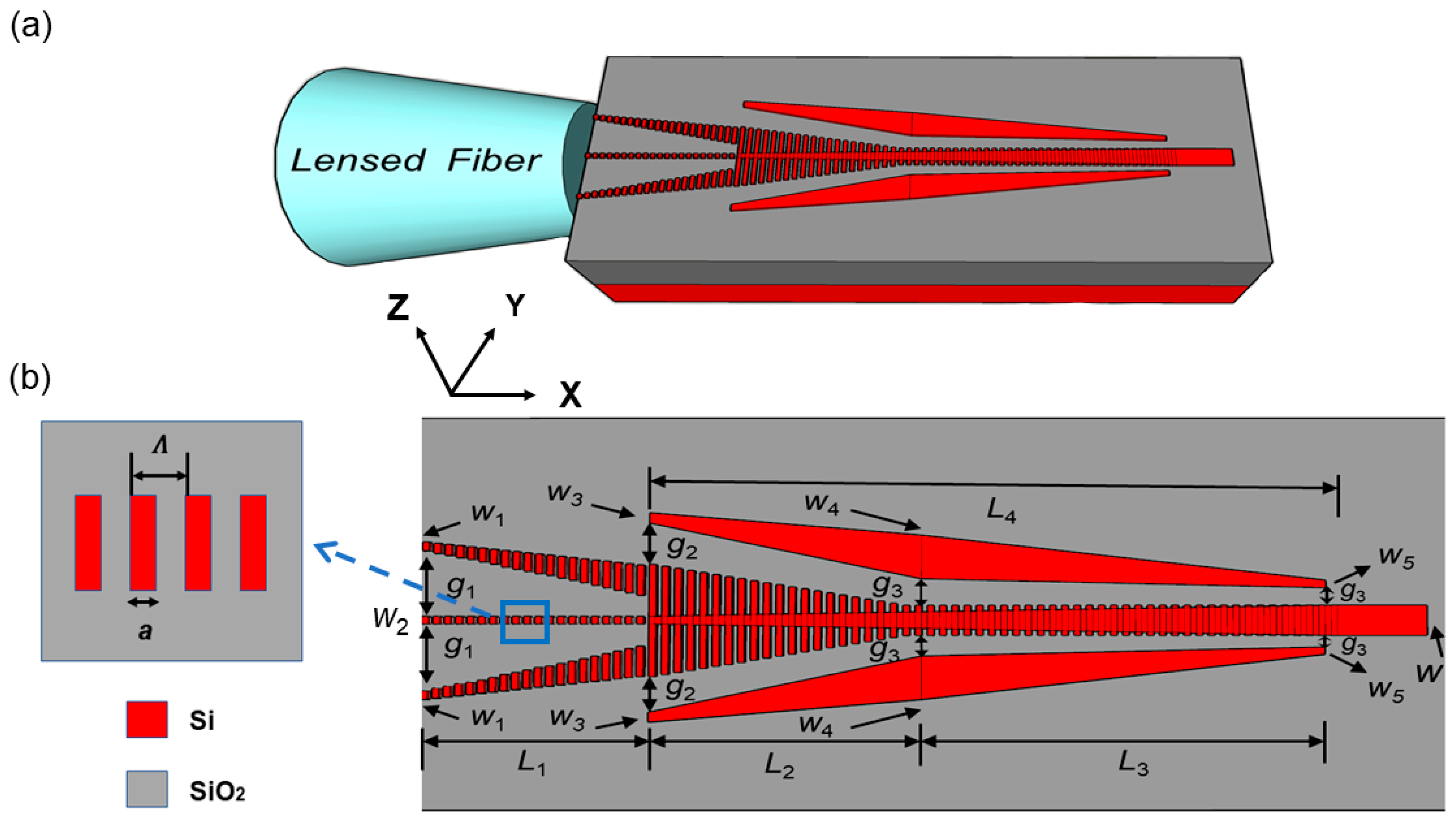
Figure 1 shows the schematic of the proposed fiber-to-chip edge coupler. The key conversion region is composed of one trident-shaped SWG in the center and two matched strip waveguides on both sides along the propagation direction (
x-direction). As the light launches into the edge coupler from the lensed fiber, it is firstly coupled and guided by the trident-shaped SWG to reduce the mode size, where the tip widths at the interface side are set as
W1 (=120 nm) and
W2 (=160 nm) with a gap width of
g1 between them and the coupling length is
L1 (part 1), respectively. At the end of coupling length
L1, the tip widths on both sides are linearly increased to 450 nm, while the tip width in the center remains unchanged (
W2 = 160 nm), where the gap width is reduced to 80 nm between them. Secondly, the trident-shaped SWG is gradually turned into the taper SWG in order to further shrink the coupled mode size together with two matched silicon waveguides on both sides, where the coupling length along the
x-direction is
L2 (part 2) and the tip width and gap width of the silicon waveguide are
W3 (
W4) and
g2 (
g3) at the left side (right side), respectively. The corresponding width of taper SWG structure is tapered from 1.22 μm to 0.45 μm. Thirdly, the SWG-wire tapered transition structures are employed to couple the optical mode from SWG waveguide to output silicon wire waveguide, and the bilateral matched strip waveguides are linearly tapered from
W4 to
W5 in a conversion length of
L3 (part 3), where the gap widths between bilateral strip waveguides and central SWG-wire tapered waveguide are kept the same (
g3 = 150 nm) along the
x-direction. Note that, to enhance the mode conversion efficiency, a tapered silicon wire waveguide is used in the central part of the tapered SWG from left side of
L2 to right side of
L3, corresponding to the waveguide width tapering from 160 nm to 450 nm. Therefore, the total conversion length is a sum of
L1,
L2, and
L3. Through these three key steps, the input fiber mode (lensed fiber, MFD: 3.2 μm [
15,
26]) can be efficiently converted to on-chip silicon waveguide mode with a typical waveguide size of 220 nm × 450 nm, which is a commonly used size for the on-chip single-mode silicon waveguide. In addition, the grating period and duty cycle of the employed SWG structure are set as Λ = 300 nm and a/Λ = 50%, respectively, which could alleviate the fabrication requirements.
Based on the abovementioned device scheme, a three-dimensional finite-difference time-domain (3D-FDTD) method is employed to design and optimize the device parameters in detail [
29,
30].
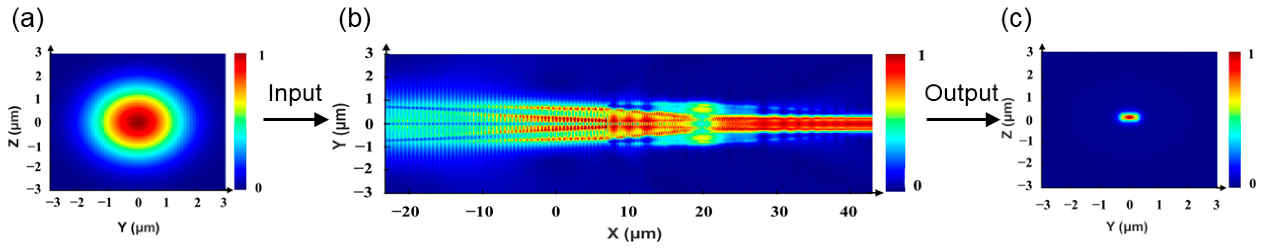
Figure 2 illustrates the calculated light field evolution through the designed device. We can clearly find that the input fiber mode is indeed converted to the silicon waveguide mode in a total conversion length of 60 μm, and the area difference between input and output modes is quite large (over 100 times) from results of the electric field distributions shown in
Figure 2a,c. Utilizing the proposed edge coupler, the input fiber mode size is gradually reduced as well as enhanced mode power density. By adding two matched strip waveguides on both sides of the central SWG waveguide, the coupled mode could be well-confined in the taper SWG region and further converted to the silicon waveguide via SWG-wire tapered transition waveguide. Finally, we can obtain an efficiently fundamental TE
0 mode of the single-mode silicon waveguide, achieving fiber-to-chip coupling requirements. Within this process, the coupling loss is mainly from the interface between the optical fiber and proposed edge coupler. To reduce such loss, the mode field match should be designed as high as possible at the interface, which is determined by the mode overlap between optical fiber and coupler facet. The mode overlap (MO) is given by [
27,
28]
where
Eo and
Ec represent the electric field distributions of optical fiber mode and waveguide mode at the interface, and
A is the 2D integral region, respectively. To achieve high coupling efficiency, the mode of the designed waveguide structure at the interface should overlap with the fiber mode to a great extent. After the mode field match, stable and low-loss light transmission and mode conversion should be required to obtain an efficient on-chip fiber-to-chip coupler. Therefore, we will perform detailed structure design and optimization to find the optimum device parameters in the following sections.
3. Results
Before we conduct the structural parameter analyses, the device performance index should be determined first. For the fiber-to-chip edge coupler, loss is a key indicator which includes coupling loss and transmission loss [
26,
27,
28]. Here, we employ IL coming from input fiber mode to output silicon waveguide mode to characterize the device performance.
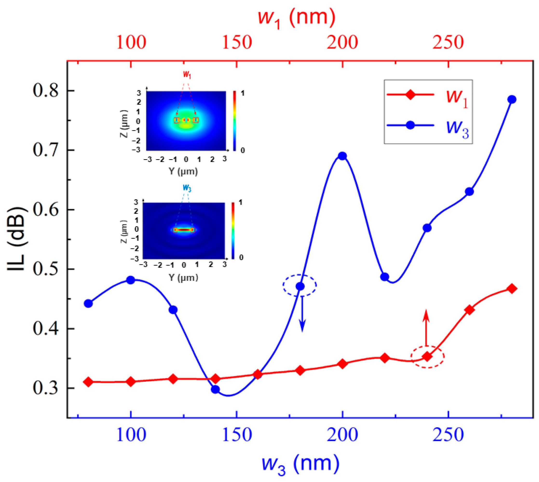
Figure 3 shows the obtained IL of the proposed edge coupler as functions of the tip widths (
W1,
W3) at the left side of part 1 and part 2. It is noted that the tip width
W3 of the matched silicon strip waveguide has more influence on the device performance than the tip width
W1 of the trident-shaped SWG, where the optimum value of
W3 is 140 nm within the calculation range. Meanwhile, we can find that the tip width
W1 will almost not affect the device performance (IL) as its value is less than 180 nm, which corresponds to a high mode overlap between optical fiber mode and waveguide mode at the coupling interface. Furthermore, the corresponding electric field distributions can be observed in the insets of
Figure 3. Therefore, by consideration of the obtained IL and fabrication linewidth requirement, we set
W1 as 120 nm in the following analyses.
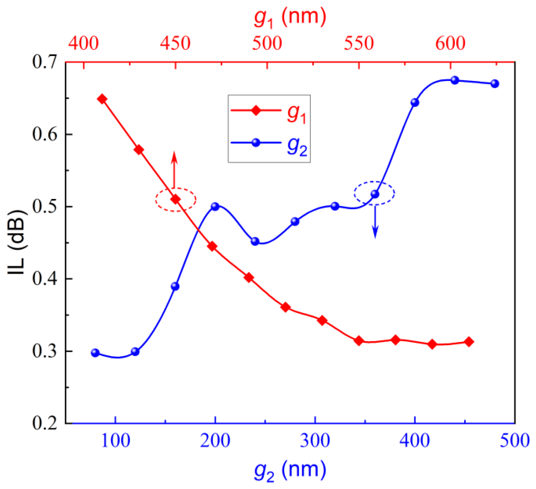
Apart from tip widths of SWG and silicon waveguide, their gap widths (
g1,
g2) are also closely related to the device performance.
Figure 4 plots the gap widths (
g1,
g2) variation affecting the IL, where
g1 and
g2 are the gap widths at the left side of part 1 and part 2, respectively. From
Figure 4, we can observe that the obtained IL is gradually reducing as
g1 increases from 420 nm to 620 nm, and the IL tends to be stable when
g1 is larger than 550 nm, revealing a high mode overlap with input fiber mode achieved at this gap position. Here, we choose
g1 as 570 nm, which could be easily realized via using current fabrication facilities [
28,
31]. However, for
g2, nearly opposite changing behavior can be found, that is, the large gap width will bring large on-chip coupling loss. To reduce IL, a small gap width of
g2 is recommended, and
g2 is set as 120 nm in the present device by consideration of the device fabrication. The corresponding device IL is about 0.3 dB at these chosen optimum positions. Moreover, the required conversion length of every part in the proposed edge coupler should be also determined, which is related to the total fiber-to-chip conversion length.
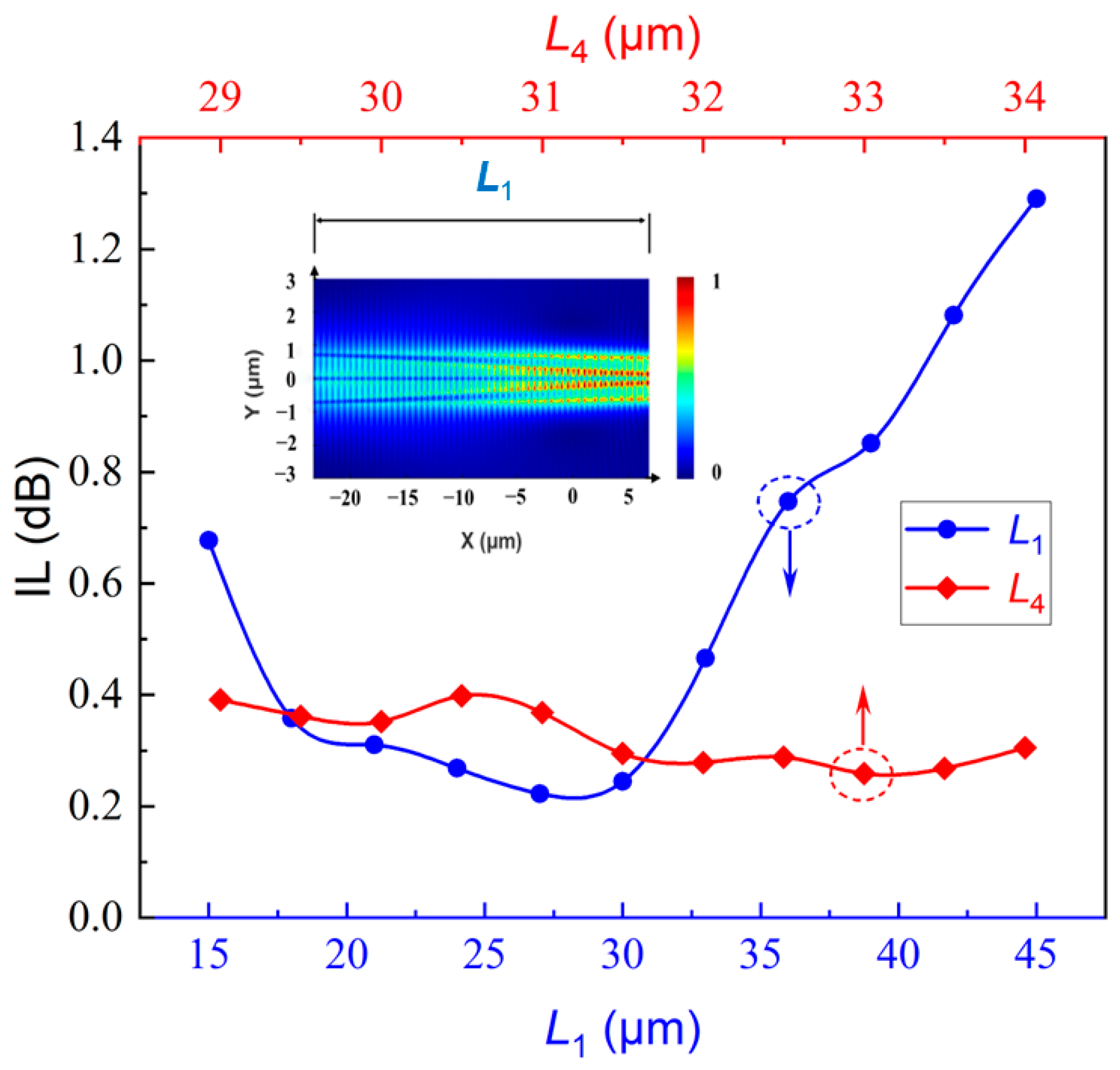
Figure 5 shows the obtained IL dependent on the conversion lengths of part 1 (
L1) and part 2 + part 3 (
L4 =
L2 +
L3) in the proposed device. Here, we consider part 2 and part 3 as a whole during calculation, and more detailed optimizations on their lengths are performed in
Figure 6. From
Figure 5, we can clearly find a low loss range for the conversion length
L1, that is, from 18 μm to 30 μm with IL lower than 0.4 dB. Within such a range, the obtained lowest IL is only 0.23 dB at the conversion length
L1 = 27 μm, which is quite promising for the low-loss fiber-to-chip coupler. Meanwhile, IL reveals relatively low dependence on the conversion length
L4 and
L4 is a combination of
L2 and
L3. As
L4 varies from 31.5 μm to 34 μm, the obtained IL is relatively stable and the lowest value is nearly 0.25 dB at the conversion length around
L4 = 33 μm. Therefore, the obtained ultralow-loss feature of the proposed edge coupler as well as quite short conversion length offers a good solution for the light coupling between optical fiber and on-chip silicon waveguide compared with previous reports [
19,
20,
21,
22,
23,
26,
27,
28].
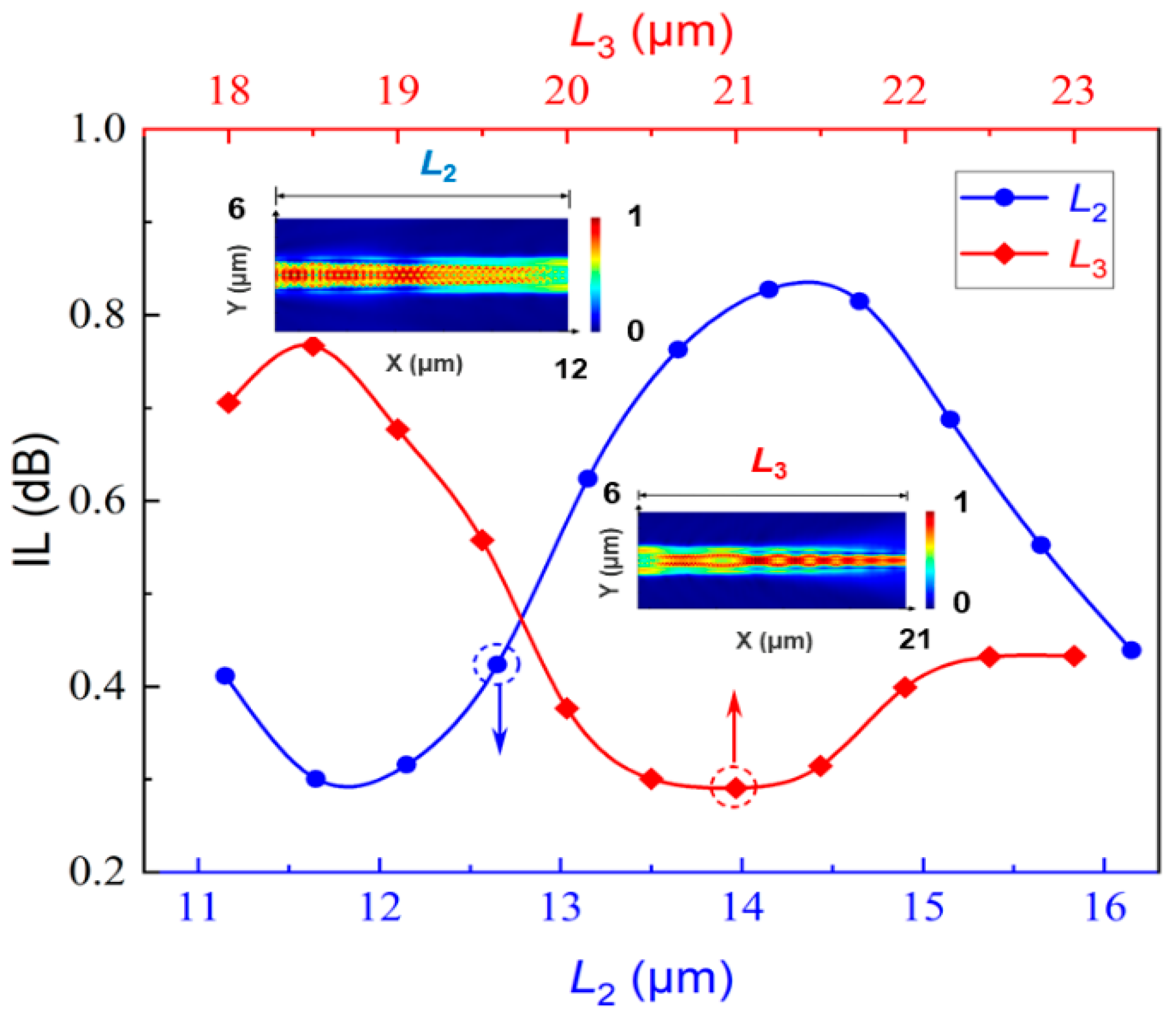
Figure 6 gives a more detailed analysis of device performance (IL) dependent on the conversion lengths
L2 and
L3 of part 2 and part 3 in the proposed device. From
Figure 6, we can find obvious fluctuations within the calculation ranges and the ranges we chose can cover the lowest value of IL. To obtain such low IL, the optimum conversion lengths are located at
L2 = 12 μm and
L3 = 21 μm, respectively. If these conversion lengths shift from their optimum values about ±1 μm, the obtained IL is still lower than 0.4 dB, revealing relatively large fabrication tolerance. Thus, the total conversion length of the silicon waveguide structure for the edge coupler is
L1 +
L2 +
L3 = 60 μm in the length direction, which can efficiently guide the light mode from input optical fiber to the on-chip silicon waveguide, realizing the compact fiber-to-chip coupling. Moreover, the reflection loss of the proposed device is less than −28 dB, which is quite low for the on-chip devices.
Table 1 lists the final determined structural parameters of the proposed fiber-to-chip edge coupler.
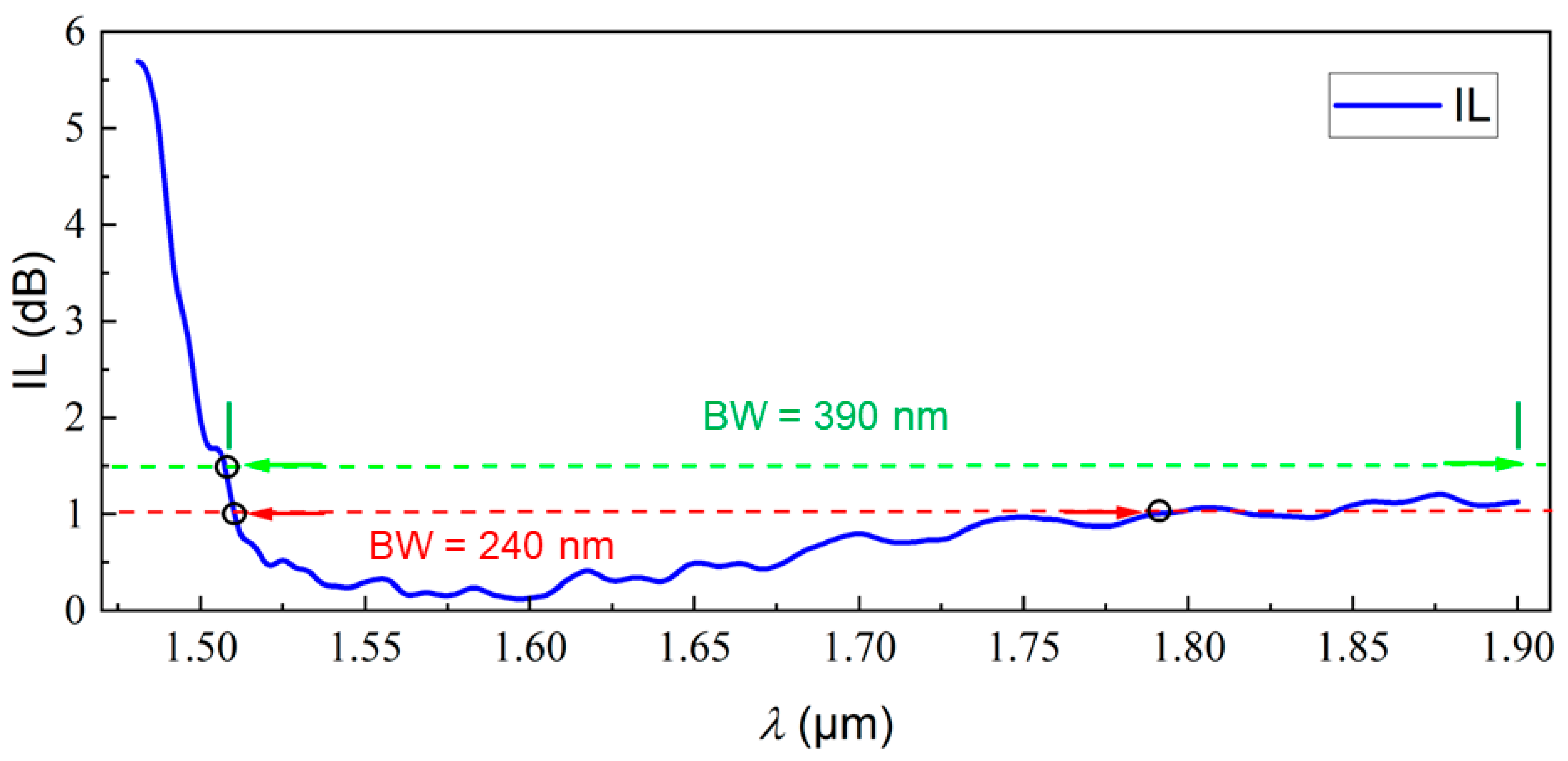
Based on the optimized structural parameters, we further study the wavelength spectrum of IL for the proposed device shown in
Figure 7, where the material dispersions of silicon and silica are also considered [
32]. Note that the device reveals better performance working at long wavelength than at the short wavelength within the calculation range from 1.48 μm to 1.9 μm. When the working wavelength is less than 1.5 μm, the device IL is quickly increased, even larger than 5 dB, which is very large for fiber-to-chip coupling loss. If we want to make IL less than 1.5 dB, the allowable working wavelength range can vary from 1510 nm to 1900 nm, corresponding to a bandwidth of 390 nm. If we further reduce the criterion of IL to 1 dB, the available working bandwidth can still reach 240 nm from 1520 nm to 1760 nm, which is superior to some previous reports [
20,
22,
23,
26,
27,
28]. Meanwhile, at the nominal wavelength of 1.55 μm, IL is quite low, only 0.23 dB. Therefore, the proposed device would be a good candidate to well support the low-loss and broadband operation of on-chip silicon devices.
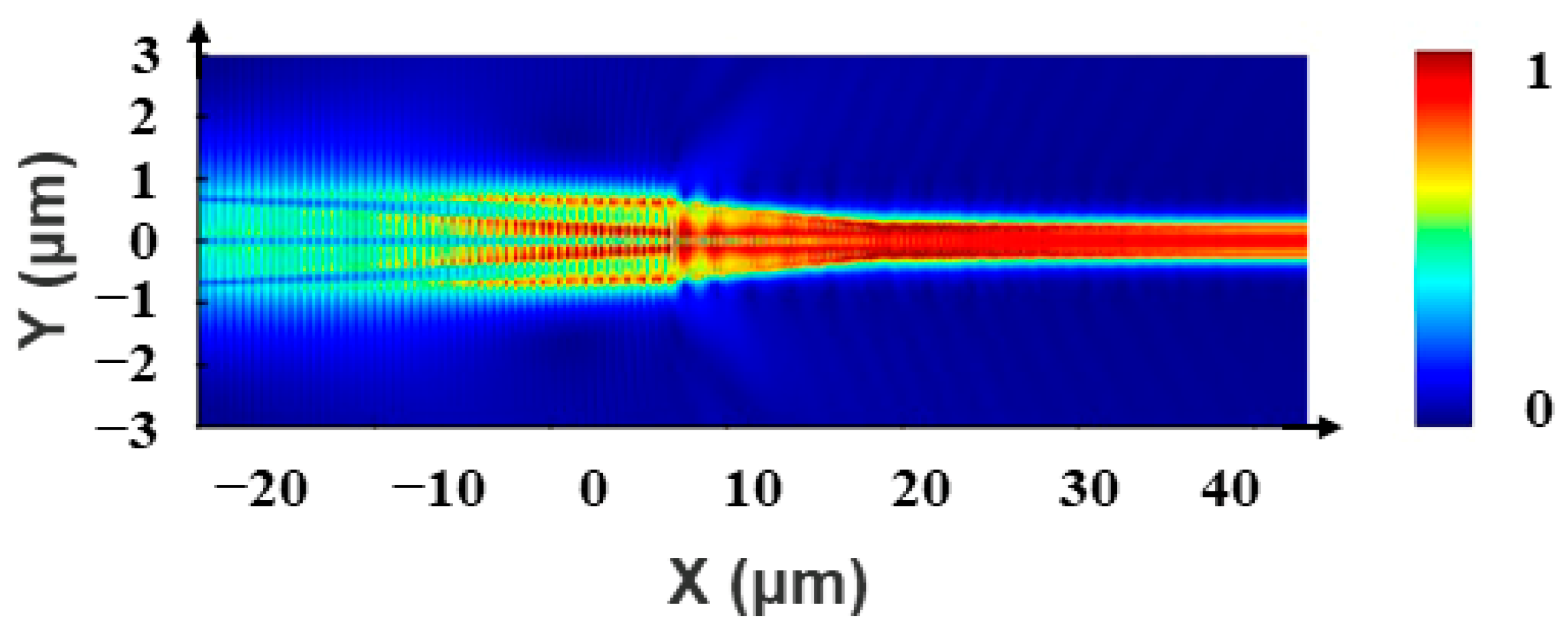
To better reveal the function of the two matched strip waveguides on both sides of the central trident-shaped SWG structure, we have made a comparison, that is, the two matched strip waveguides are missing, and the electric field evolution can be found in
Figure 8. From this figure, we can find that a slight diffraction effect can be observed at the end of part 2 and the obtained IL of such a device is 0.6 dB at the working wavelength of 1.55 μm. If we further add the designed two matched strip waveguides, such a diffraction effect can be removed as shown in
Figure 2b, and the obtained IL is reduced to only 0.23 dB at the working wavelength of 1.55 μm. Therefore, the added two matched strip waveguides can help eliminate the light diffraction effect during the mode coupling process from optical fiber to silicon waveguide through the proposed device. In addition, we also analyze the light field distribution along the waveguide thickness direction for the proposed device, where the device structural parameters are listed in
Table 1.
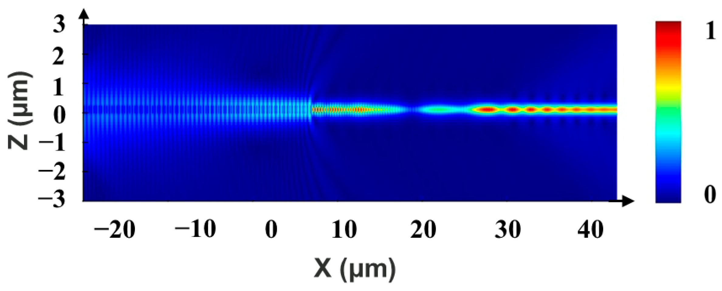
Figure 9 plots the x–z view of the electric field evolution through the designed fiber-to-chip edge coupler, where the z-direction stands for the waveguide thickness direction and both the buried oxide layer and upper cladding are silicon dioxide. From
Figure 9, we can see that the coupled light from optical fiber can be well-confined in the proposed edge coupler and no energy is leaked into the silicon substrate from our calculations.
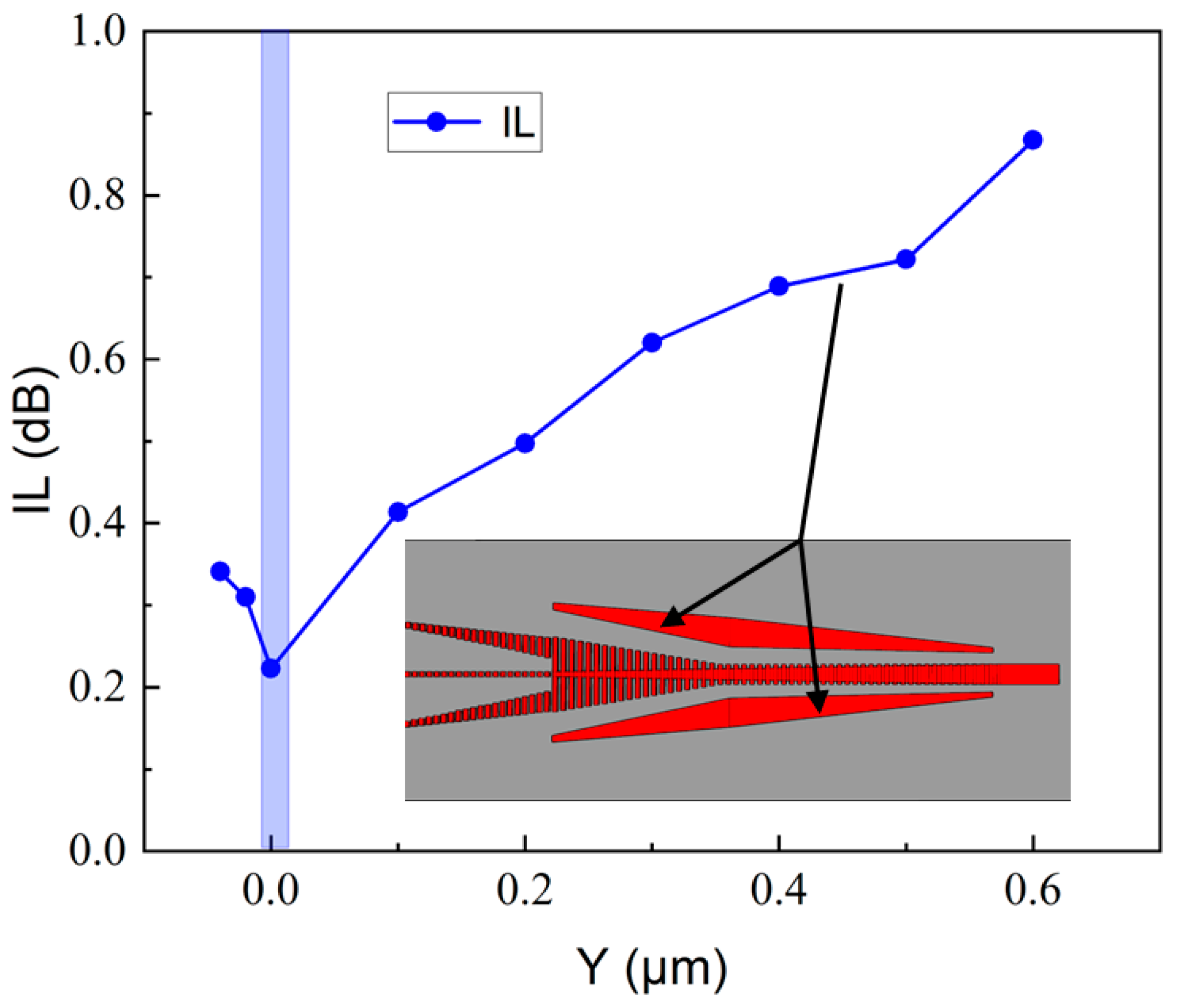
For the present device fabrication, only one-step E-beam lithography and a one-step etching process will be required since the whole device has a uniform etching depth (220 nm), which could be realized using current fabrication facilities [
15,
28,
31]. Considering fabrication imperfections in practice, we consider the lateral offset between trident-shaped SWG and two matched strip waveguides, because these two sections are separated and their relative positions are more easily affected by fabrication errors. The optimum relative positions shown in
Table 1 are derived through structural optimizations. We define Y as the lateral offset of two matched strip waveguides relative to the central trident-shaped SWG. Y = 0 stands for the optimum positions, Y > 0 stands for the two matched strip waveguides away from the central trident-shaped SWG, and Y < 0 stands for the two matched strip waveguides close to the central trident-shaped SWG, respectively, and the obtained results are shown in
Figure 10. Note that the device performance reveals significant performance deterioration when the relative positions shift from their optimum positions, particularly for Y > 0. If IL < 0.5 dB should be kept, the lateral offset range can vary from −40 nm to 200 nm according to our calculation results, which would be very friendly to the device fabrication. In addition, we have also calculated the tolerance ranges of duty cycle, tip width, and gap width of the proposed fiber-to-chip edge coupler, which are shown in
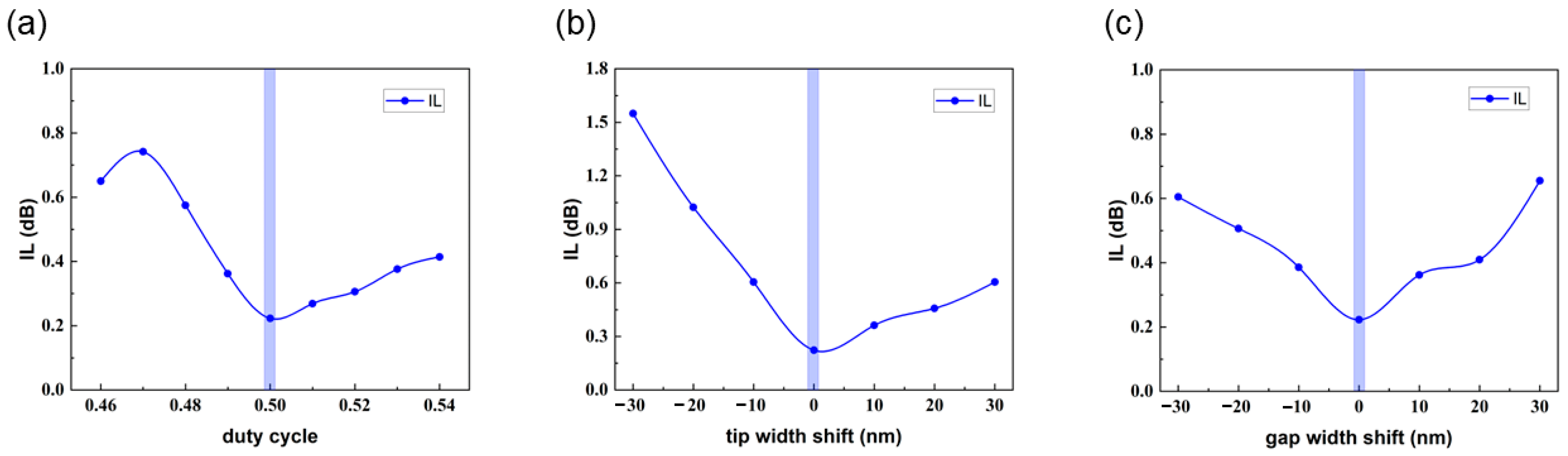
Figure 11. From this figure, we can find that the tip width of the proposed device has the smallest tolerance range compared with the duty cycle and gap width. If we set the same criterion of IL < 0.5 dB for them, the available tolerance ranges are from 0.483 to 0.540, from −8 to 24 nm, and from −20 to 25 nm for the duty cycle, tip width shift, and gap width shift, respectively. Therefore, we should carefully control the tip width of the proposed device during the device fabrication process.
Finally, we make a comprehensive comparison between previously reported fiber-to-chip edge couplers and the proposed device from total length, IL, bandwidth, and fiber mode size, as listed in
Table 2. It is indicated that the working bandwidth and IL of our proposed edge coupler are obviously better than some reported devices. Meanwhile, the total conversion length of 60 μm is also comparable to some reports and only single-step lithography and etching process will be required. With these features, we hope the proposed edge coupler could boost the development of broadband and low-loss fiber-to-chip coupler and further drive PICs towards broadband work and applications.


