An Ultra-Broadband Polarization Beam Splitter Based on the Digital Meta-Structure at the 2 µm Waveband

Abstract
:1. Introduction
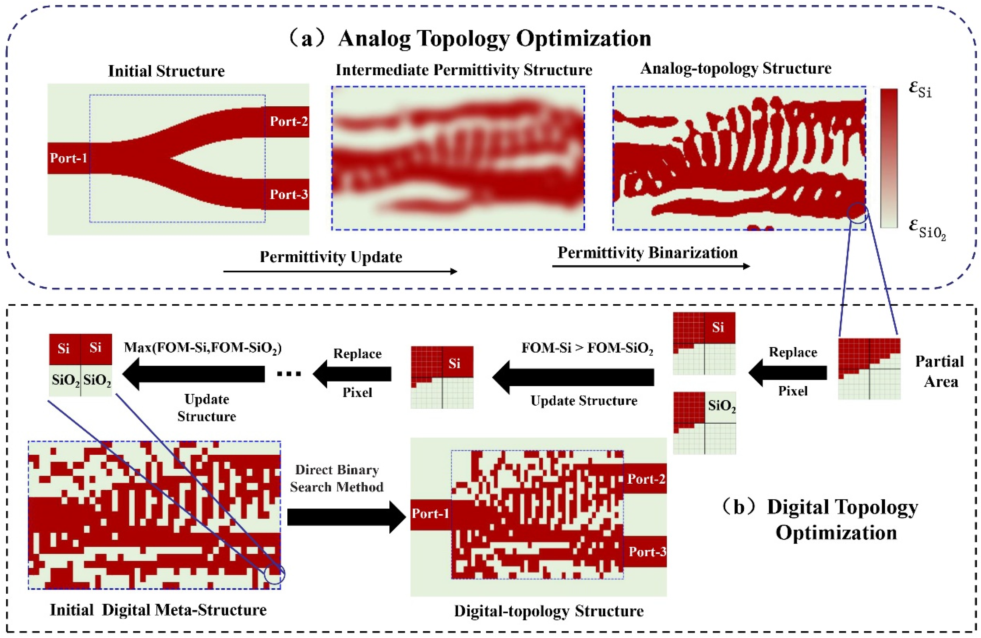
2. Device Design
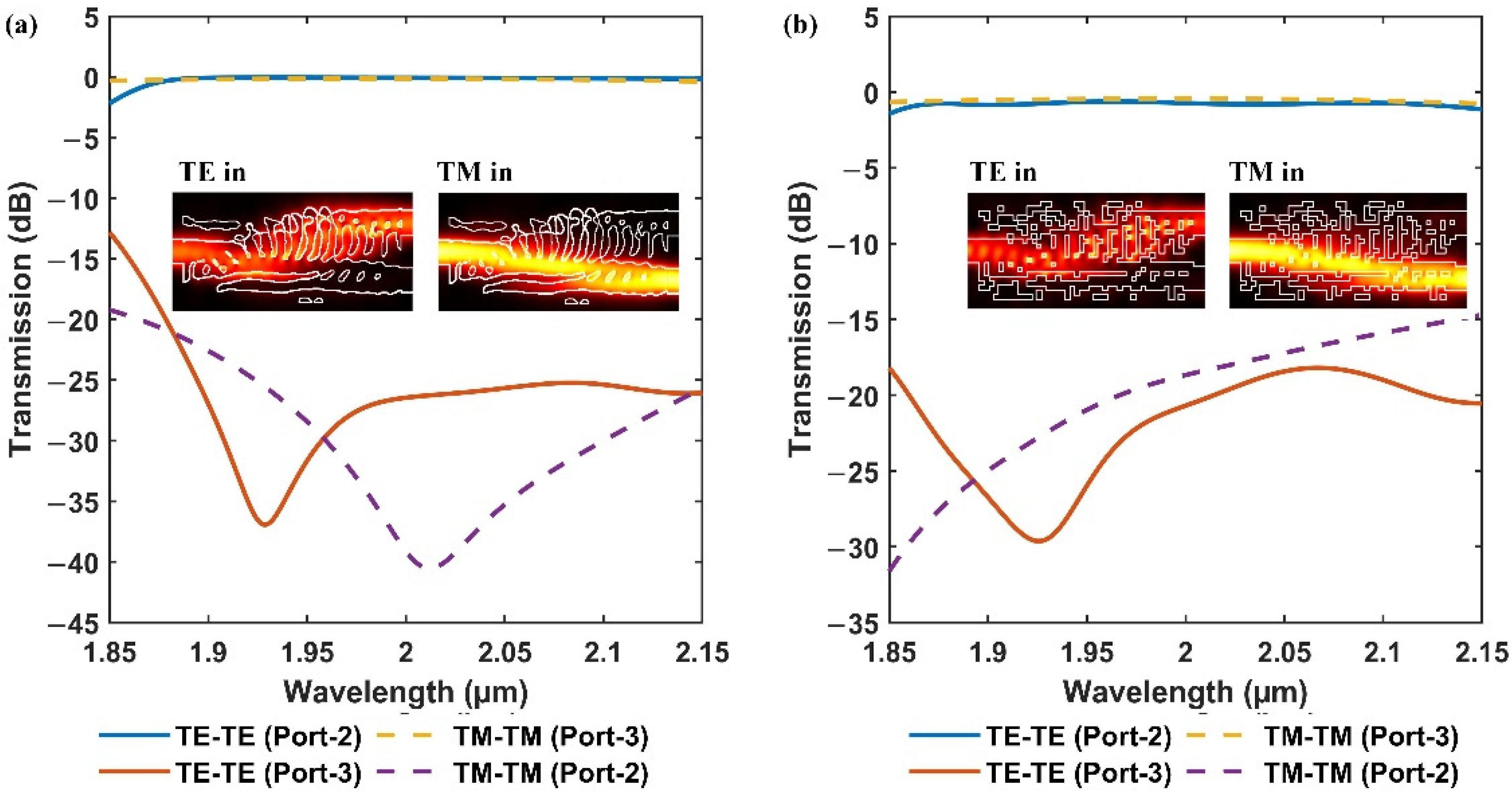
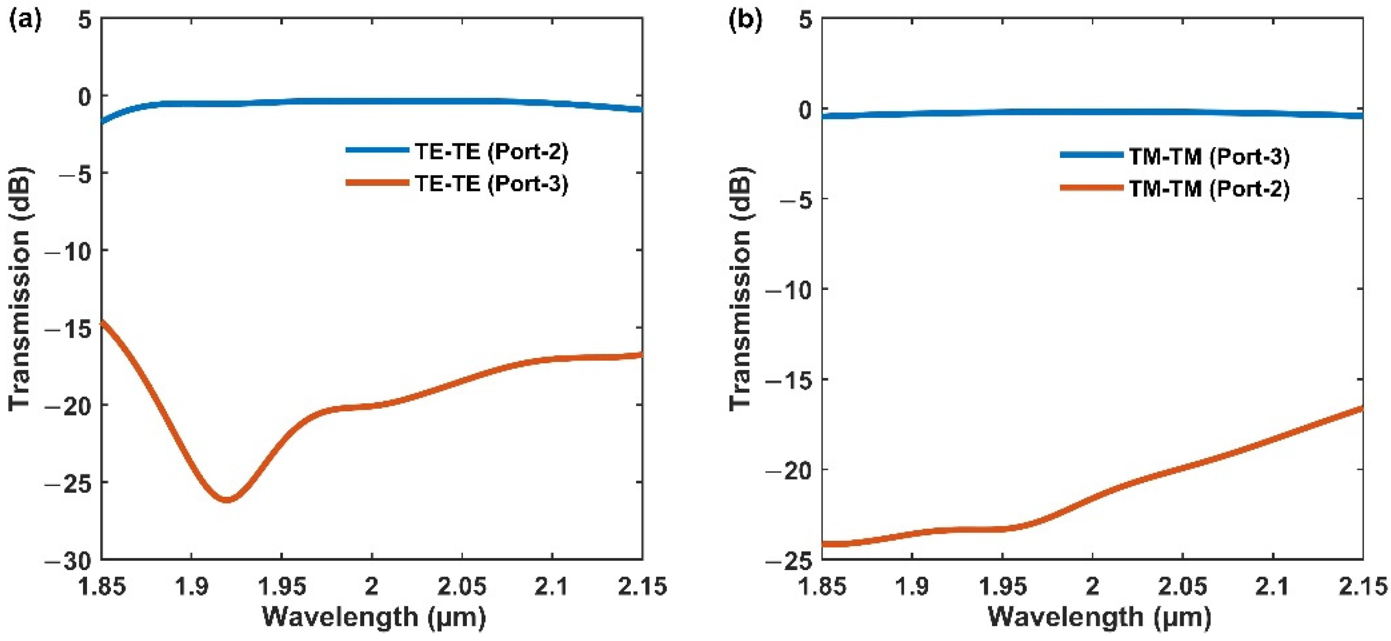
3. Results and Discussions
4. Conclusions
Author Contributions
Funding
Institutional Review Board Statement
Informed Consent Statement
Data Availability Statement
Conflicts of Interest
References
- Xu, K.; Sun, L.; Xie, Y.; Song, Q.; Du, J.; He, Z. Transmission of IM/DD signals at 2-μm wavelength using PAM and CAP. IEEE Photonics J. 2016, 8, 1–7. [Google Scholar] [CrossRef]
- Xu, K.; Wu, Q.; Xie, Y.; Tang, M.; Fu, S.; Liu, D. High speed single-wavelength modulation and transmission at 2μm under bandwidth-constrained condition. Opt. Express 2017, 25, 4528–4534. [Google Scholar] [CrossRef] [PubMed]
- Li, Z.; Heidt, A.; Simakov, N.; Jung, Y.; Daniel, J.; Alam, S.U.; Richardson, D. Diode-pumped Wideband Thulium-doped Fiber Amplifiers for Optical Communications in the 1800–2050 nm Window. Opt. Express 2013, 21, 26450–26455. [Google Scholar] [CrossRef] [PubMed] [Green Version]
- Shen, W.; Du, J.; Sun, L.; Wang, C.; Zhu, Y.; Xu, K.; Chen, B.; He, Z. Low-Latency and High-Speed Hollow-Core Fiber Optical Interconnection at 2-Micron Waveband. J. Lightwave Technol. 2020, 38, 3874–3882. [Google Scholar] [CrossRef]
- Liu, Z.; Chen, Y.; Li, Z.; Kelly, B.; Phelan, R.; O’Carroll, J.; Bradley, T.; Wooler, J.P.; Wheeler, N.V.; Heidt, A.M.; et al. High-capacity directly modulated optical transmitter for 2-μm spectral region. J. Lightwave Technol. 2015, 33, 1373–1379. [Google Scholar] [CrossRef] [Green Version]
- Dong, Y.; Wang, W.; Xu, S.; Lei, D.; Gong, X.; Guo, X.; Wang, H.; Lee, S.Y.; Loke, W.K.; Yoon, S.F.; et al. Two-micron-wavelength germanium-tin photodiodes with low dark current and gigahertz bandwidth. Opt. Express 2017, 25, 15818–15827. [Google Scholar] [CrossRef]
- Van Camp, M.A.; Assefa, S.; Gill, D.M.; Barwicz, T.; Shank, S.M.; Rice, P.M.; Topuria, T.; Green, W.M. Demonstration of electrooptic modulation at 2165nm using a silicon Mach-Zehnder interferometer. Opt. Express 2012, 20, 28009–28016. [Google Scholar] [CrossRef]
- Cao, W.; Hagan, D.; Thomson, D.J.; Nedeljkovic, M.; Littlejohns, C.G.; Knights, A.; Alam, S.U.; Wang, J.; Gardes, F.; Zhang, W.; et al. High-speed silicon modulators for the 2 μm wavelength band. Optica 2018, 5, 1055–1062. [Google Scholar] [CrossRef]
- Wang, X.; Shen, W.; Li, W.; Liu, Y.; Yao, Y.; Du, J.; Song, Q.; Xu, K. High-speed silicon photonic Mach–Zehnder modulator at 2 μm. Photonics Res. 2021, 9, 535–540. [Google Scholar] [CrossRef]
- Shen, L.; Huang, M.; Zheng, S.; Yang, L.; Peng, X.; Cao, X.; Li, S.; Wang, J. High-Performance Silicon 2 × 2 Thermo-Optic Switch for the 2-μm Wavelength Band. IEEE Photonics J. 2019, 11, 1–6. [Google Scholar]
- Ruan, Z.; Shen, L.; Zheng, S.; Wang, A.; Long, Y.; Zhou, N.; Wang, J. Subwavelength grating slot (SWGS) waveguide at 2 μm for chip-scale data transmission. Nanophotonics 2018, 7, 865–871. [Google Scholar] [CrossRef]
- Zheng, S.; Huang, M.; Cao, X.; Wang, L.; Ruan, Z.; Shen, L.; Wang, J. Silicon-based four-mode division multiplexing for chip-scale optical data transmission in the 2 μm waveband. Photonics Res. 2019, 7, 1030–1035. [Google Scholar] [CrossRef]
- Li, J.; Liu, Y.; Meng, Y.; Xu, K.; Du, J.; Wang, F.; He, Z.; Song, Q. 2 μm Wavelength Grating Coupler, Bent Waveguide, and Tunable Microring on Silicon Photonic MPW. IEEE Photonics Technol. Lett. 2018, 30, 471–474. [Google Scholar] [CrossRef]
- Xie, H.; Liu, Y.; Sun, W.; Wang, Y.; Xu, K.; Du, J.; He, Z.; Song, Q. Inversely designed 1 × 4 power splitter with arbitrary ratios at 2-μm spectral band. IEEE Photonics J. 2018, 10, 1–6. [Google Scholar] [CrossRef]
- Guan, X.; Wu, H.; Shi, Y.; Dai, D. Extremely small polarization beam splitter based on a multimode interference coupler with a silicon hybrid plasmonic waveguide. Opt. Lett. 2014, 39, 259–262. [Google Scholar] [CrossRef]
- Xu, L.; Wang, Y.; Kumar, A.; Patel, D.; El-Fiky, E.; Xing, Z.; Li, R.; Plant, D.V. Polarization beam splitter based on MMI coupler with SWG birefringence engineering on SOI. IEEE Photonics Technol. Lett. 2018, 30, 403–406. [Google Scholar] [CrossRef]
- Xu, L.; Wang, Y.; El-Fiky, E.; Mao, D.; Kumar, A.; Xing, Z.; Saber, M.G.; Jacques, M.; Plant, D.V. Compact broadband polarization beam splitter based on multimode interference coupler with internal photonic crystal for the SOI platform. J. Lightwave Technol. 2019, 37, 1231–1240. [Google Scholar] [CrossRef]
- Lin, Z.; Chen, K.; Huang, Q.; He, S. Ultra-Broadband Polarization Beam Splitter Based on Cascaded Mach-Zehnder Interferometers Assisted by Effectively Anisotropic Structures. IEEE Photonics J. 2021, 13, 1–9. [Google Scholar] [CrossRef]
- Zou, J.; Yu, Y.; Zhang, X. Two-dimensional grating coupler with a low polarization dependent loss of 0.25 dB covering the C-band. Opt. Lett. 2016, 41, 4206–4209. [Google Scholar] [CrossRef]
- Zhang, Z.; Chen, X.; Cheng, Q.; Khokhar, A.Z.; Zhang, Z.; Yan, X.; Huang, B.; Chen, H.; Liu, H.; Li, H.; et al. Two-dimensional apodized grating coupler for polarization-independent and surface-normal optical coupling. J. Lightwave Technol. 2020, 38, 4037–4044. [Google Scholar] [CrossRef]
- Zou, J.; Yu, Y.; Zhang, X. Single step etched two dimensional grating coupler based on the SOI platform. Opt. Express 2015, 23, 32490–32495. [Google Scholar] [CrossRef] [PubMed]
- Dai, D.; Bowers, J.E. Novel ultra-short and ultra-broadband polarization beam splitter based on a bent directional coupler. Opt. Express 2011, 19, 18614–18620. [Google Scholar] [CrossRef] [PubMed]
- Wang, X.; Quan, X.; Zhang, W.; Hu, J.; Shen, C.; Cheng, X. Ultra-small and fabrication-tolerant silicon polarization beam splitter using sharp bent directional coupler. IEEE Photonics J. 2018, 10, 1–7. [Google Scholar] [CrossRef]
- Fu, P.H.; Huang, T.Y.; Fan, K.W.; Huang, D.W. Optimization for ultrabroadband polarization beam splitters using a genetic algorithm. IEEE Photonics J. 2018, 11, 1–11. [Google Scholar] [CrossRef]
- Shen, B.; Wang, P.; Polson, R.; Menon, R. An integrated-nanophotonics polarization beamsplitter with 2.4 × 2.4 μm2 footprint. Nat. Photonics 2015, 9, 378–382. [Google Scholar] [CrossRef]
- Liu, X.; Liu, D.; Dai, D. Silicon polarization beam splitter at the 2 μm wavelength band by using a bent directional coupler 166 assisted with a nano-slot waveguide. Opt. Express 2021, 29, 2720–2726. [Google Scholar] [CrossRef]
- Lalau-Keraly, C.M.; Bhargava, S.; Miller, O.D.; Yablonovitch, E. Adjoint shape optimization applied to electromagnetic design. Opt. Express 2013, 21, 21693–21701. [Google Scholar] [CrossRef] [Green Version]
- GitHub. Scipy/Scipy/ at v1.8.0. Available online: https://github.com/scipy/scipy/tree/v1.8.0 (accessed on 18 April 2022).
- Zhou, M.; Lazarov, B.S.; Wang, F.; Sigmund, O. Minimum length scale in topology optimization by geometric constraints. Comp. Methods Appl. Mech. Eng. 2015, 293, 266–282. [Google Scholar] [CrossRef] [Green Version]
- Zhang, G.; Liboiron-Ladouceur, O. Scalable and low crosstalk silicon mode exchanger for mode division multiplexing system enabled by inverse design. IEEE Photonics J. 2021, 13, 1–13. [Google Scholar] [CrossRef]
- Wen, X.; Xu, K.; Song, Q. Design of a barcode-like waveguide nanostructure for efficient chip–fiber coupling. Photonics Res. 2016, 4, 209–221. [Google Scholar] [CrossRef]
- Xu, K.; Liu, L.; Wen, X.; Sun, W.; Zhang, N.; Yi, N.; Sun, S.; Xiao, S.; Song, Q. Integrated photonic power divider with arbitrary power ratios. Opt. Lett. 2017, 42, 855–858. [Google Scholar] [CrossRef] [PubMed] [Green Version]
- Taflove, A. Application of the finite-difference time-domain method to sinusoidal steady-state electromagnetic-penetration problems. IEEE Trans. Electromagn. Compat. 1980, 3, 191–202. [Google Scholar] [CrossRef]
- Lu, L.; Liu, D.; Zhou, F.; Li, D.; Cheng, M.; Deng, L.; Fu, S.; Xia, J.; Zhang, M. Inverse-designed single-step-etched colorless 3 dB couplers based on RIE-lag-insensitive PhC-like subwavelength structures. Opt. Lett. 2016, 41, 5051–5054. [Google Scholar] [CrossRef] [PubMed]
- Augenstein, Y.; Rockstuhl, C. Inverse design of nanophotonic devices with structural integrity. ACS Photonics 2020, 7, 2190–2196. [Google Scholar] [CrossRef]
- Su, L.; Piggott, A.Y.; Sapra, N.V.; Petykiewicz, J.; Vuckovic, J. Inverse design and demonstration of a compact on-chip narrowband three-channel wavelength demultiplexer. ACS Photonics 2018, 5, 301–305. [Google Scholar] [CrossRef] [Green Version]
- Piggott, A.Y.; Ma, E.Y.; Su, L.; Ahn, G.H.; Sapra, N.V.; Vercruysse, D.; Netherton, A.M.; Khope, A.S.; Bowers, J.E.; Vuckovic, J. Inverse-designed photonics for semiconductor foundries. ACS Photonics 2020, 7, 569–575. [Google Scholar] [CrossRef]
- Xu, H.; Dai, D.; Shi, Y. Ultra-broadband and ultra-compact on-chip silicon polarization beam splitter by using hetero-anisotropic metamaterials. Laser Photonics Rev. 2019, 13, 1800349. [Google Scholar] [CrossRef]
- Herrero-Bermello, A.; Dias-Ponte, A.; Luque-González, J.M.; Ortega-Moñux, A.; Velasco, A.V.; Cheben, P.; Halir, R. Experimental demonstration of metamaterial anisotropy engineering for broadband on-chip polarization beam splitting. Opt. Express 2020, 28, 16385–16393. [Google Scholar] [CrossRef]
- Li, C.; Zhang, M.; Bowers, J.E.; Dai, D. Ultra-broadband polarization beam splitter with silicon subwavelength-grating waveguides. Opt. Lett. 2020, 45, 2259–2262. [Google Scholar] [CrossRef]


| Reference | Year | Footprint (μm2) | TM Mode | TE Mode | BW * (nm) | Waveband | ||
|---|---|---|---|---|---|---|---|---|
| EL (dB) | PER (dB) | EL (dB) | PER (dB) | |||||
| Xu et al. [38] | 2019 | 12.25 × 1.9 | <0.9 | >20 | <0.2 | >20 | 215 | 1.55-µm |
| Herrero-Bermello et al. [39] | 2020 | 92.4 × 4 | <1.0 | >20 | <1.0 | >20 | 130 | 1.55-µm |
| Li et al. [40] | 2020 | 33.6 × 4.04 | <0.3 | >20 | <0.3 | >20 | 270 | 1.55-µm |
| Lin et al. [18] | 2021 | 198.3 × 2.8 | <0.5 | >20 | <0.5 | >20 | 310 | 1.55-µm |
| Liu et al. [26] | 2021 | 48 × 10 | <0.5 | >15 | <0.02 | >30 | 195 | 2-µm |
| Our Work | 5.4 × 2.52 | <0.33 | >18.1 | <0.53 | >16.5 | 216 | 2-µm | |
Publisher’s Note: MDPI stays neutral with regard to jurisdictional claims in published maps and institutional affiliations. |
© 2022 by the authors. Licensee MDPI, Basel, Switzerland. This article is an open access article distributed under the terms and conditions of the Creative Commons Attribution (CC BY) license (https://creativecommons.org/licenses/by/4.0/).
Share and Cite
Xu, J.; Liu, Y.; Guo, X.; Du, J.; Xu, K. An Ultra-Broadband Polarization Beam Splitter Based on the Digital Meta-Structure at the 2 µm Waveband. Photonics 2022, 9, 361. https://doi.org/10.3390/photonics9050361
Xu J, Liu Y, Guo X, Du J, Xu K. An Ultra-Broadband Polarization Beam Splitter Based on the Digital Meta-Structure at the 2 µm Waveband. Photonics. 2022; 9(5):361. https://doi.org/10.3390/photonics9050361
Chicago/Turabian StyleXu, Jiefeng, Yingjie Liu, Xiaoyuan Guo, Jiangbing Du, and Ke Xu. 2022. "An Ultra-Broadband Polarization Beam Splitter Based on the Digital Meta-Structure at the 2 µm Waveband" Photonics 9, no. 5: 361. https://doi.org/10.3390/photonics9050361