Article

Ultra-Sensitive Si-Based Optical Sensor for Nanoparticle-Size Traditional Water Pollutant Detection

1
Department of Electrical Engineering, University of Business and Technology, Jeddah 21432, Saudi Arabia
2
Department of Engineering Mathematics and Physics, Alexandria University, Alexandria 21544, Egypt
3
Department of Computer Science and Engineering, University of Bridgeport, 221 University Ave., Bridgeport, CT 06604, USA
*
Author to whom correspondence should be addressed.
Photonics 2022, 9(5), 289; https://doi.org/10.3390/photonics9050289
Submission received: 21 March 2022 / Revised: 17 April 2022 / Accepted: 21 April 2022 / Published: 23 April 2022
(This article belongs to the Special Issue Optical Sensing)

Abstract

:
A low-cost Si-based optical nano-sensor that monitors traditional water pollutants is introduced in this paper. The introduced sensor works in the near-infrared region, 900 nm to 2500 nm spectral range. The proposed structure consists of a Si layer with an optimized thickness of 300 nm on the top of the Al layer acting as a back reflector. On the top of the Si layer, the water pollutants are modeled as nanoparticle materials of different sizes. The finite difference time domain method is utilized to optimize the thicknesses of the Si layer by analyzing the optical light absorption considering different Si layer thicknesses and different pollutant nanoparticles’ sizes. Different interpolation techniques, including polynomials with various degrees and locally weighted smoothing quadratic regression, are used to find the best fitting model representing the simulated data points with goodness of fit analysis. Three features are proposed to identify the water pollutant with its size, peak absorption wavelength, relative amplitude, and a full width at half maximum. The device’s performance in detecting six different pollutants, silver, aluminum, copper, chromium, selenium, and ammonia, is evaluated. Sensitivity, a figure of merit, and a quality factor are used to evaluate the proposed sensor. The obtained maximum sensitivity is 11,300 nm/RIU, FOM of 740, and quality factor of 670.

1. Introduction

Human daily activities have increased water pollution, and water sources deteriorate yearly [1]. Common water pollutants include nitrate (NO3, and NH3+), fluoride (F), and heavy metals “iron (Fe), Pb (lead), Cd (cadmium), Cr (chromium), Ni (nickel), Zn (zinc), Sb (antimony), As (arsenic), Hg (mercury), etc.” [2]. As the concentration of these pollutants increases, they severely affect human health. This attracts researchers’ attention to develop techniques to monitor and treat water pollutants. There are several techniques used to detect water pollutants. One of the old methods is the separation of pollutants using the chromatography technique. It is a very sensitive method for the detection of pollutants but a very expensive technique and needs complicated tools [3,4]. Furthermore, electrochemical techniques are also used to detect pollutants, especially those that are non-UV-absorbing analytes. This technique detects an electric current in a cell generated by a chemical oxidation or reduction process [5,6]. With the rapid progress in the field of semiconductor optical devices, another technique that depends on fluorescence has been adopted because of its high sensitivity, fast detection, and low cost [7,8]. Additionally, graphene quantum dots with gold plasmonic particles are used in the pollutant detection process using localized surface plasmon resonance (LSPR) interaction between graphene and the plasmonic particles [9,10]. Gold nanoparticles with ZnO nanoparticles on the surface of tapered optical fiber are utilized to detect p-cresol in water. ZnO is a direct bandgap semiconductor material and is used to improve the biocompatibility of the sensor as it helps in binding the enzyme over the sensor [11].
Moreover, silver nanoparticles in optical sensors are used for water pollutant detection by measuring the changes in the peak wavelength and shape of the spectrum curve due to the presence of the pollutants [12]. Silver nanoparticles have a lower cost and higher extinction coefficients than gold nanoparticles. The high molar extinction coefficient of silver nanoparticles leads to improved visibility based on the difference in optical brightness and increased sensitivity of UV-visible spectroscopic detection [13].
Nanostructure-based devices are used as SPR sensors. Si-based sensors that use layers of Si, silver (Ag), and aluminum oxide (Al2O3) grating are reported to be a highly sensitive device (sensitivity of 477 nm/RIU, and FOM of 38) in an optical communication band from 1400 to 1550 nm [14]. Additionally, Si nanowire Field Effect Transistor (FET) sensors with gold nanoparticles are reported to have enhanced NH3-sensing characteristics and long-term reliability [15].
In this work, we introduced a highly sensitive Si-based water pollutant ultra-thin optical nano-sensor that operates in the NIR region, 11,300 nm/RIU. The following sections are organized as follows: first, the sensors’ performance metrics are introduced; second, the proposed sensor for water pollutant detection is presented; and finally, the simulation results, optimizing the sensor design and its performance evaluation, are discussed.

2. Sensor Performance Excellence Indicators and the Proposed Structure

As reported in the literature, the performance indicators for sensor evaluation are the refractive index sensitivity (RIS), full width at half maximum (FWHM), and figure of merit (FOM). The RIS of a sensor is defined in terms of the shift in peak wavelength (∆λ) per the change in the surrounding medium refractive index ‘refractive index (n) unit’ (RIU) [16]. The refractive index sensitivity is given by:
R I S = Δ λ Δ n
Another characterization factor to determine the quality of sensors is the spectral resolution. The resolution is determined by the linewidth and the intensity of the spectral peak and is represented by the FWHM of the spectral peak. A narrow peak helps recognize a peak shift and enhances detection accuracy. Another performance indicator is the figure of merit, which indicates the sensor’s performance by combining sensitivity and FWHM of sensing spectrum [17,18], calculated using Equation (2).
F O M = R I S F W H M
One more parameter is the quality factor (Q-factor) which is defined as the ratio of peak wavelength (λmax) to the FWHM [16,17,18]. Large Q-factor values represent the high selectivity of the sensor. The quality factor is given by:
Q = λ m a x F W H M
The peak wavelength (λmax) depends on the dielectric of the surrounded medium and relative permittivity of the nanoparticles and is given by:
λ m a x = P n ( ε P ε m ( λ m a x ) ε m + ε P ( λ m a x ) ) 1 / 2
where εm is the permittivity of the surrounding medium, εP is a plasmonic NP dielectric constant at corresponding λmax, n is an integer, and P is structural periodicity.
The dielectric permittivity can be expressed by using a multi-oscillator Drude–Lorentz model [19] as given in Equation (5):
ε p l a s m o n i c = ε ω D 2 ω 2 + j ω γ D k = 1 6 δ k ω k 2 ω 2 ω k 2 + 2 j ω γ k  
where ε is the plasmonic high frequency dielectric permittivity, ωD and γD are the plasma and collision frequencies of the free electrons, δk is the amplitude of Lorentz oscillator, ωk is the resonance angular frequencies and γk is the damping constants (k = 1,2,…, 6).
On the other hand, the proposed structure is designed, optimized, and analyzed using an electromagnetic wave solver, Lumerical Finite Difference Time Domain (FDTD) solutions software in the near-infrared region. The proposed model contains a single unit cell parametrized by a Si layer of a varying cross-section area from 1 × 10⁴ nm2 to 1 × 10⁶ nm2 and thickness, d, optimized to 300 nm. A thick Al layer is used on the bottom of the Si layer, acting as a back reflector and ohmic contact. The back reflector layer is used to enhance light trapping and reflects the transmitted light from the silicon layer to the structure for more light absorption [20,21]. The schematic diagram is shown in Figure 1. The Si layer is the platform for the water pollutants nanoparticle modeled as spherical nanoparticles (NPs) with a radius varying from 50 nm to 500 nm. The spherical shape has some advantages over other shapes as they are highly symmetrical particles with mono-dispersity and synthetic reproducibility. It is reported that the spherical shape gives the best absorption properties [22].
In the simulation of a unit cell, the boundary conditions are considered as a periodic structure in x and y directions, and the layers are perfectly matched in z-direction. A plane wave source with a wavelength band 500–3000 nm is used as a light source, and the minimum mesh size is 0.5 nm in all directions with an offset time of 7.5 fs used for the light source. The absorption of the nanoparticles is measured at different wavelengths. We started the optimization process by adding plasmonic Au NPs on the Si platform layer. Plasmonic NPs such as Au and Ag have shape- and size-dependent optical properties, so they are widely used to fabricate water pollutant sensors [23,24,25]. The absorption spectrum is measured, and accordingly, the Si layer thickness maximizing the absorption is recorded. In the results section, optimizing the layer thickness is detailed. As a result of optimization, the thickness is selected to be 300 nm, and this thickness maximizes the variation in maximum absorption wavelength shift as a function of the particle radius. The sensor’s performance depending on the absorption spectrum peak wavelength, FWHM, and absorption intensity is characterized and illustrated below.
Then, the performance of the designed sensor is studied in detecting other common water pollutants such as Ag, Al, Cu, Cr, Se, and NH3. Furthermore, the quality indicators, which are sensor sensitivity (RIS), the figure of merit (FOM), and quality factor (Q) are calculated.
The refractive indices of plasmonic NPs used in the simulation are summarized in Table 1 [26]. They are calculated using Equation (5). The refractive index of silicon is a function of the wavelength and is characterized by the Aspnes and Studna model [27], while selenium is characterized by Ciesielski et al.’s model [28]. Chromium follows Rakić et al.’s model [29], and NH3 refractive index is characterized by Clive Cuthbertson and Maude Cuthbertson’s model [30].

3. Results and Discussion

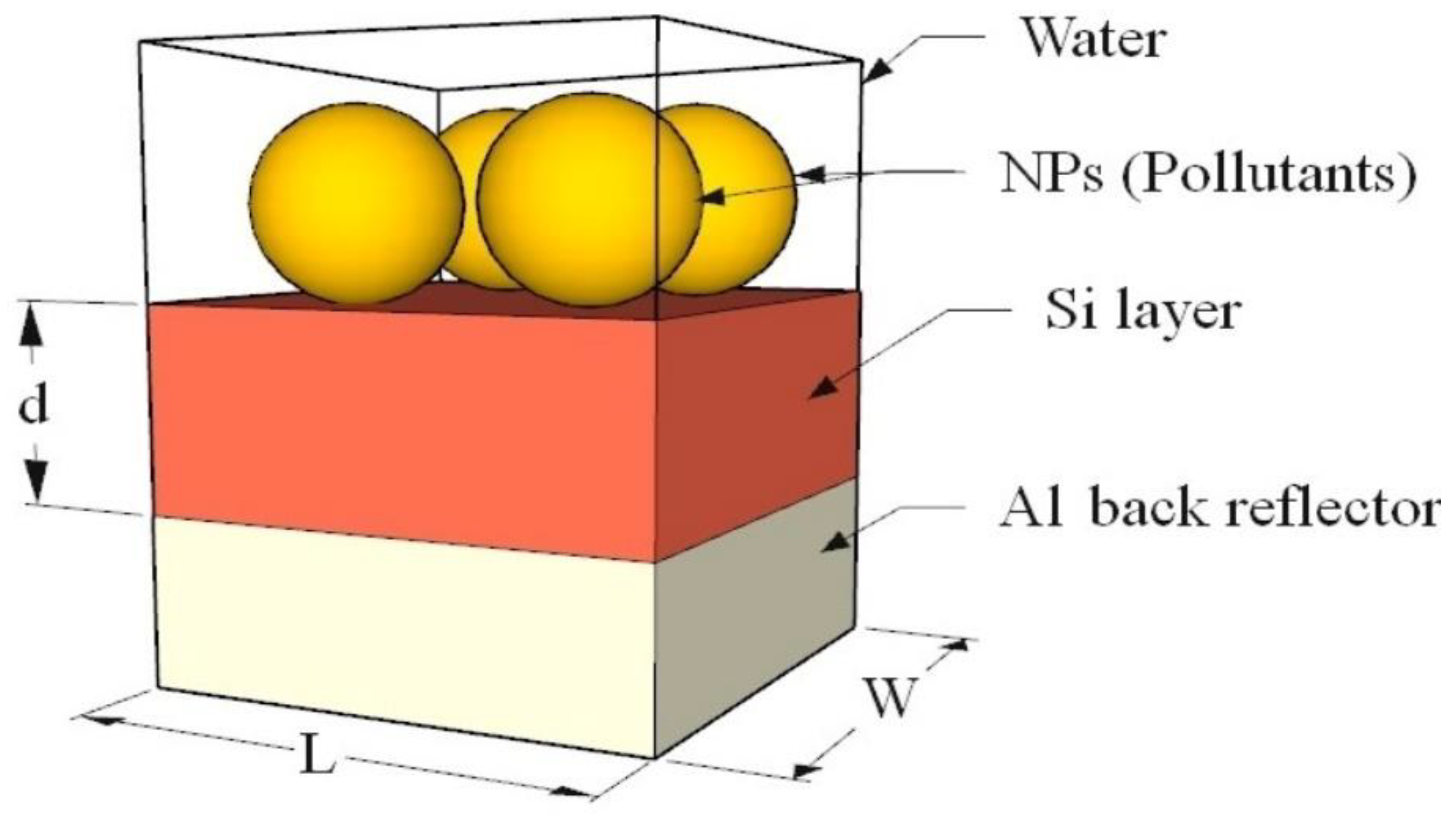
In this section, the optimization of the Si layer thickness is given, then the device’s performance in detecting various water pollutants is evaluated. Furthermore, the ability of the device to detect more than one water pollutant existing simultaneously is discussed.

3.1. Optimizing Si Layer Thickness

The device has been simulated for different thicknesses of the Si layer, d , and with different Au NP sizes. The Si layer has been changed from 100 nm to 500 nm in a step of 100 nm, while the Au NP radius, r, takes the following values (50 nm, 100 nm, 200 nm, 300 nm, 400 nm, and 500 nm). In the simulation, it is assumed that the Au spherical NPs are touching each other with no separation between them. The absorption spectrum of the device is measured, and the peak wavelength (λmax), peak amplitude (I), and the FWHM of the absorption curve have been recorded for each case.
The absorbed light spectrum is shown in Figure 2 with Au NP of radius 50 nm, 200 nm, and 400 nm when the Si layer is 300 nm thick. This is a sample of the measured spectrum where only three full-spectrum curves are selected to display the obtained absorption behavior. The absorption spectral shapes reveal that each NP size has size-dependent absorption characteristics, considering that the NP absorption cross-section depends on the Au NP size. Changing the NP size does not only change the peak wavelength but also changes the FWHM and relative intensity of the absorption spectrum. Figure 3 shows a sample of the absorbed power distribution around the Au NP and in the Si layer for NPs of radius 500 nm at its maximum absorption wavelength (λmax = 2.1 μm) and at a minimum absorption wavelength. It is clear from 
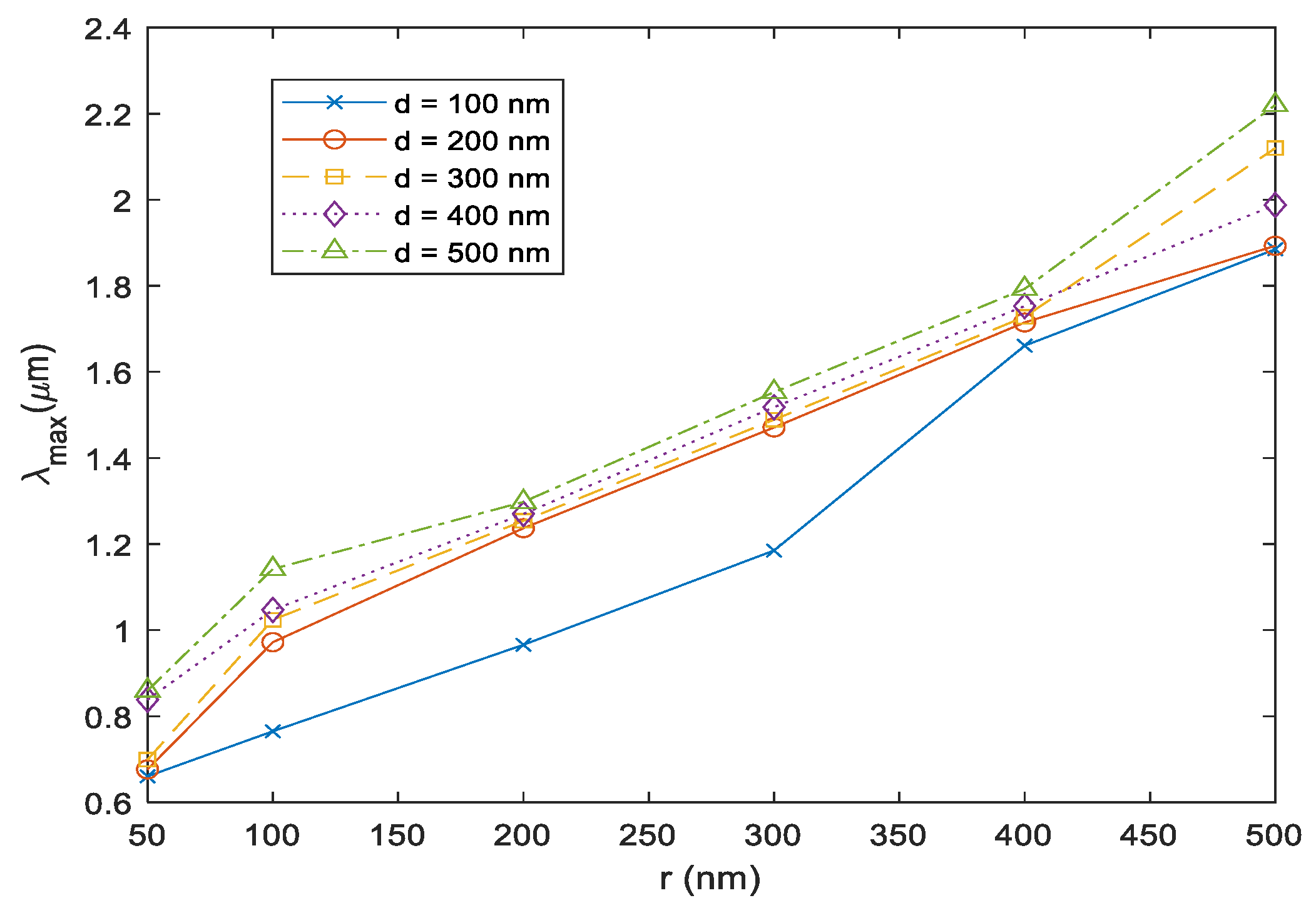
Figure 3a that the absorption power increases at the resonance wavelength of the Au NP, which increases the overall absorption of the sensor. The peak wavelength variation depending on the Au NP’s size (50 nm, 100 nm, 200 nm, 300 nm, 400 nm, and 500 nm) is shown in Figure 4 for unoptimized Si layer thickness that varies from 100 to 500 nm. The observed absorption peak wavelength (λmax) is redshifted as the size of the Au NP increases for all Si layer thickness values. This behavior is expected as the resonance wavelength of the Au plasmons is tunable depending on the particle shape, size, and number [31]. When irradiated with electromagnetic waves, the metal NPs oscillate with size-dependent Eigen frequencies. This feature results from the confinement of the electron cloud at the metal-Si layer boundary. Using the Drude–Sommerfeld model of the dielectric function of the NP metal shows that plasmons resonance wavelength shifts to a longer wavelength as the size of the NP increases [32,33]. This NP behavior eventually leads to the size-dependent optical and electronic properties that could be optimized to suit devices applications by varying the nanoparticle size.
The dependence of the FWHM and absorption intensity on the size of the Au NPs and the thickness of the Si layer is shown in Table 2. The data shows that the shape of the absorption curve varies depending on both the nanoparticle size and the thickness of the Si layer.
For all Si layer thickness values, FWHM and relative intensity seem to be distinct for each particle size, i.e., each particle size has a spectral shape that varies depending on the size. From the obtained data and encouraged by the systematic variation of the peak absorption wavelength, we elected the peak absorption wavelength as the parameter that will be used to optimize the Si layer thickness to maximize the shift in λmax as a function of the particle radius. This will increase the sensitivity of the sensor to NP size variations.
To optimize the Si layer thickness, an equation governing the peak absorption wavelength as a function of nanoparticle radius and Si layer thickness needs to be generated. Different interpolation techniques are adopted, including polynomials with various degrees and locally weighted smoothing quadratic regression (LOESS) to generate the required equation [34]. These techniques have been utilized to find the best fitting models of the simulated data points shown in Figure 4. The optimum model is selected based on the goodness of fit criterion considering the following statistics:
  • Sum of squares due to error (SSE)
SSE measures the deviation in the fitted model as defined by Equation (6):
S S E = i = 1 n w i ( y i y ^ i ) 2
where w i is the weights while y i and the y ^ are the actual data and the interpolated ones, respectively [35]. A model with good fitting is when SSE is close to 0.
2.
R-Square
The metric indicates how well the fit describes the variability. It is defined as the proportion of the sum of squares of the regression (SSR) and the total sum of squares (SST). SSR is defined as:
S S R = i = 1 n w i ( y ^ i y ¯ i ) 2
SST is defined as the sum of squares that deviated from the mean and is defined as
S S T = i = 1 n w i ( y i y ¯ i ) 2
where SST = SSR + SSE. R-square is defined as:
R - Square = S S R S S T = 1 S S E S S T
R-Square can take values between 0 and 1, with a value close to 1 representing a good fitting model.
3.
Adjusted R-Square
The adjusted R-Square is defined by:
Adjusted   R - Square = 1 S S E ( n 1 ) v
where n is defined as the number of response values and v is the residual degrees of freedom defined by the difference between n and the number of fitted coefficients estimated from the response values. The static can take any value between 0 and 1, with a value close to 1 representing a good fitting model.
4.
Root Mean Squared Error (RMSE)
It is defined as the square root of the mean square error (MSR). Again, a model with a value close to zero will represent a good fitting model.
Applying the previously mentioned interpolation techniques, the peak location of the maximum light absorption as a function of Si layer thickness d and the Au NP radius, r, is modeled by a polynomial of degree 5 as given by Equation (11):
λ m a x ( d , r ) = p 00 + p 10 × d + p 01 × r + p 20 × d 2 + p 11 × d × r + p 02 × r 2 + p 30 × d 3 + p 21 × d 2 × r + p 12 × d × r 2 + p 03 × r 3 + p 40 × d 4 + p 31 × d 3 × r + p 22 × d 2 × r 2 + p 13 × d × r 3 + p 04 × r 4 + p 41 × d 4 × r + p 32 × d 3 × r 2 + p 23 × d 2 × r 3 + p 14 × d × r 4 + p 05 × r 5
where d is normalized by a mean of 300 nm and standard deviation (std) of 143.8 nm and r is normalized by a mean of 258.3 nm and std of 161.9 nm. The goodness of fit metrics is given in Table 3. The recorded goodness of fit is the best result obtained when trying different interpolation techniques. The goodness of fit parameters is in the acceptable range, which indicates the high accuracy of the fitting equation.
The coefficients of the fitted polynomial using the adjusted R-square method with 95% confidence bounds are given in Table 4. The coefficients shown are selected in the middle of the 95% confidence interval shown.
The fitted surface of λ m a x   ( d , r ) shown in Figure 5 depicts that λ m a x is monotonically increasing as a function of both the radius and the Si layer thickness. The residuals plot in Figure 5 indicates small interpolation errors between the actual data points and the fitted surface.
The gradient of the fitted surface, δ λ m a x / δ r is calculated and plotted in Figure 6. The optimized thickness of the Si layer is determined from the maximum of the gradient. This optimum point is marked in Figure 6, and it is found that the optimum thickness is 285 nm. This is the optimum thickness to detect the smallest used Au NP, r = 50 nm with size sensitivity δ λ m a x / δ r = 8.36 . So, the proposed structure Si layer thickness was set to 300 nm. By maximizing the size sensitivity of the device, the absorption peak wavelength could be used to detect the particle size with high sensitivity as there is no overlap between the different peaks.
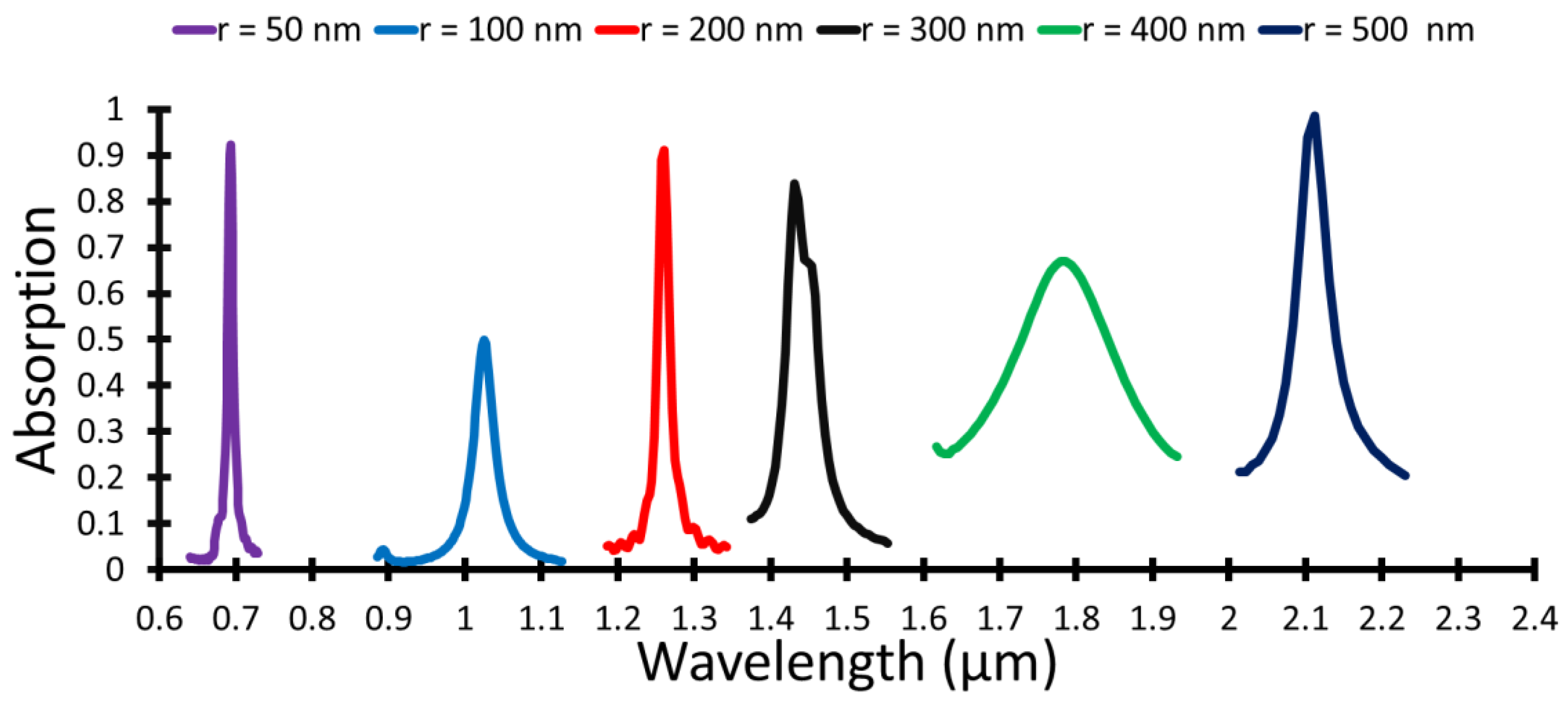
The spectral peaks shown in Figure 7 are obtained using the optimum Si layer thickness. These spectral peaks are truncated from the full absorption spectrum shown in Figure 2 to illustrate the different features of the spectral peaks for all Au NPs sizes. There is a suitable wavelength span between each spectral peak as we maximized the size sensitivity of the device.
The effect of the concentration of Au NP on the peak wavelength is investigated, and it is observed that the peak wavelength redshifts as the number of Au NP increases. Additionally, the spectrum broadens as the concentration of the Au NP increases. Figure 8 shows the dependence of the peak wavelength on the number of nanoparticles for the case where the Au NPs are of radius 200 nm and the Si layer thickness is 300 nm. The redshift of the spectrum with the increase of the number of nanoparticles is due to the coupling between different particles, which changes the electric field intensity on the surface. This causes a change in the oscillation frequency of the electrons, generating different cross-sections for the optical properties, including absorption and scattering [36,37,38]. The increased broadening in the absorption spectrum is attributed to both the surface scattering of electrons as well as increased radiation damping [33,39,40].

3.2. Sensitivity, FOM, and Q-factor

Equations (1)–(3) are utilized to calculate the sensitivity of the sensor, its FOM and Q-factor for different Au NP sizes. Maximizing the size selectivity of the device δ λ m a x / δ r = 8.36 , i.e., with a 300 nm thick Si layer, maximum sensitivity, FOM, and Q-factor are 3010 nm/RIU, 300, and 32, respectively. This sensitivity is higher than the reported values for the sensitivities of Au NP sensors [12,14,41,42]. The high value of the sensitivity enables the sensor to detect very small variations in the refractive index, and the high values of the FOM and Q-factor indicated that the device has good selectivity as it has a narrow FWHM.

3.3. Detecting Water Pollutants Using the Designed Optimized Sensor

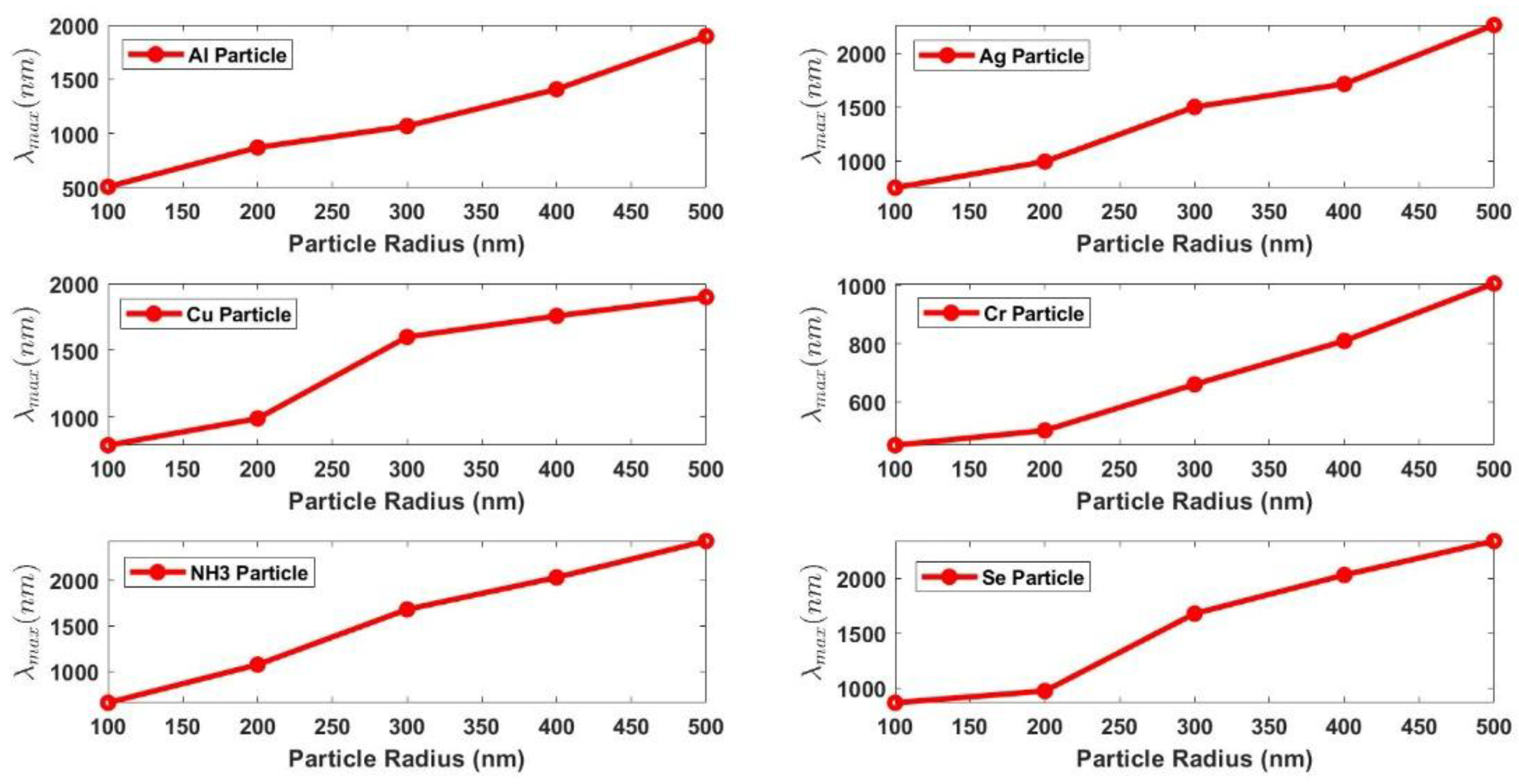
The designed Si-based sensor’s performance in detecting different sizes of water pollutants is investigated. The Au NPs on the top of the Si layer are replaced with six common water pollutants, Ag, Al, Cu, Cr, Se, and NH3. As in the case of Au NPs, the absorption spectra are measured for different sizes ranging from 100 nm to 500 nm in a step of 100 nm. The spectrum curve’s peak wavelength, FWHM, and relative intensity are observed. Figure 9 shows that the peak wavelength redshifts with the increase of the size of the pollutants. All the six pollutants’ absorption spectrum show the same behavior but with different size selectivity δ λ m a x / δ r , this is indicated by the different gradients of the six shown curves. The selectivity, δ λ m a x / δ r , takes the values from 2 to 7, which indicates the good selectivity of the sensor.
The FWHM and peak amplitude of the spectral absorption curves are shown in Table 5a,b. The results for the six pollutants show that the absorption spectral shapes have a wide variation in FWHM values that are size dependent. These variations could be favorable as pollutants could be detected depending on the peak wavelength and the shape of the absorption spectrum, FWHM, and peak relative amplitude.
Figure 10 allocates all the simulated particles with different materials and different sizes. A good separation between the detected particles with different sizes is demonstrated, and the proposed structure can differentiate between these different cases. The zooming on the plotted graph shows that there is a potential that the particles can be detected efficiently. Additionally, we have normalized the features to be from 0 to 1 and plot the 3D feature space of the detected particles along with different sizes in Figure 11. Again, it still shows a good separation between the different particles.
The sensor detection parameters are then calculated from Equations (1)–(3). The calculated values for the sensitivity, FOM, and Q-factor are presented in Table 6. Our Sensitivity is comparable with the reported value for Ag, which is about 5000 nm/RIU, but our maximum sensitivity (11,300 nm/RIU) is much higher [43]. Sharp spectral curves accompany this ultimate value of sensitivity in the case of Se that is indicated from the low values for FWHM in Table 5 and large FOM values (750) in Table 6.

3.4. More Than One Pollutant at a Time

The performance of the sensor in detecting more than one pollutant when they exist simultaneously in the water sample is studied. Pollutants are added as a couple on the surface of the Si layer, and the absorption spectral parameters, peak wavelength, FWHM, and peak wavelength relative amplitude are observed. The radius of each particle is set to 200 nm. The obtained selectivity parameters are shown in Table 7.
As the table shows, two distinct peaks at different wavelengths are observed for each couple. Each peak represents the location of one of the impurities, and each impurity has its own curve characteristics (peak location, FWHM, and peak amplitude). The first row in Table 6 shows that the peak wavelength of Au blueshifts a little from 1250 nm (peak location when Au was alone) to 1130 nm, while the Ag peak remains almost at the same location. This indicates that the peak locations could be used in the detection of pollutants even if more than one pollutant exists simultaneously.

3.5. Performance Comparision of the Proposed Sensor to Other Reported Sensors

A comparison of the performance of our sensor with the reported SPR sensors’ performance is listed in Table 8. The listed performance indicators show that the proposed sensor has much higher sensitivity than the reported values. Beside high sensitivity, the proposed sensor structure has a low cost, and it is easily fabricated.

4. Conclusions

A low-cost optical Si-based optical sensor for water pollutant detection is introduced in this paper. The device performance is optimized by maximizing the size selectivity of the device for Au NP. The optimum Si layer thickness, 300 nm, results in maximum size selectivity δ λ m a x / δ r = 8.36 . The performance parameters of the device, sensitivity, FOM, and Q-factor, are calculated. This is done for Au NP as well as other common water pollutants, Ag, Al, Cu, Cr, Se, and NH3. The optical Si-based sensor has a high sensitivity, FOM, and Q-factor of 11,300 nm/RIU, 740, and 670, respectively. These ultimate values indicate the ability of the sensor to differentiate between different nanoparticles of different sizes.

Author Contributions

Conceptualization, A.E.; methodology, A.E.; software, A.Y.; validation, A.E. and A.Y.; formal analysis, A.E.; investigation, A.Y.; data curation, A.E.; writing—original draft preparation, A.E.; writing—review and editing, K.E.; visualization, A.Y.; supervision, A.E.; project administration, K.E. All authors have read and agreed to the published version of the manuscript.

Funding

This research did not receive any funding.

Data Availability Statement

Not applicable.

Conflicts of Interest

The authors declare no conflict of interest.

References

  1. Dwivedi, A.K. Researches in water pollution: A review. Int. Res. J. Nat. Appl. Sci. 2017, 4, 118–142. [Google Scholar]
  2. Kallithrakas-Kontos, N.; Boultadaki, P.; Foteinis, S. A dataset of 112 ligands for the preconcentration of mercury, uranium, lanthanum and other pollutants and heavy metals in water. Data Brief 2020, 29, 105236. [Google Scholar] [CrossRef] [PubMed]
  3. Tian, Y.; Wei, R.; Cai, B.; Dong, J.; Deng, B.; Xiao, Y. Cationic gemini pyrrolidinium surfactants based sweeping-micellar electrokinetic chromatography for simultaneous detection of nine organic pollutants in environmental water. J. Chromatogr. A 2016, 1475, 95–101. [Google Scholar] [CrossRef] [PubMed]
  4. Portolés, T.; Pitarch, E.; López, F.J.; Hernández, F. Development and validation of a rapid and wide-scope qualitative screening method for detection and identification of organic pollutants in natural water and wastewater by gas chromatography time-of-flight mass spectrometry. J. Chromatogr. A 2011, 1218, 303–315. [Google Scholar] [CrossRef] [PubMed]
  5. Zhao, G.; Wang, H.; Liu, G. Recent advances in chemically modified electrodes, microfabricated devices and injection systems for the electrochemical detection of heavy metals: A review. Int. J. Electrochem. Sci. 2017, 12, 8622–8641. [Google Scholar] [CrossRef]
  6. Wang, L.; Peng, X.; Fu, H.; Huang, C.; Li, Y.; Liu, Z. Recent advances in the development of electrochemical aptasensors for detection of heavy metals in food. Biosens. Bioelectron. 2020, 147, 111777. [Google Scholar] [CrossRef]
  7. Gowri, A.; Kathiravan, A. Fluorescent chemosensor for detection of water pollutants. In Sensors in Water Pollutants Monitoring: Role of Material, 1st ed.; Pooja, D., Kumar, P., Singh, P., Patil, S., Eds.; Springer: Singapore, 2020; pp. 147–160. [Google Scholar]
  8. Scircle, A.; Cizdziel, J.V. Detecting and quantifying microplastics in bottled water using fluorescence microscopy: A new experiment for instrumental analysis and environmental chemistry courses. J. Chem. Educ. 2019, 97, 234–238. [Google Scholar] [CrossRef]
  9. Li, Y.; Zhu, Y.; Wang, C.; He, M.; Lin, Q. Selective detection of water pollutants using a differential aptamer-based graphene biosensor. Biosens. Bioelectron. 2019, 126, 59–67. [Google Scholar] [CrossRef]
  10. Nien, Y.H.; Su, T.Y.; Chou, J.C.; Lai, C.H.; Kuo, P.Y.; Lin, S.H.; Lai, T.Y.; Rangasamy, M. Investigation of flexible arrayed urea biosensor based on graphene oxide/nickel oxide films modified by au nanoparticles. IEEE Trans. Instrum. Meas. 2020, 70, 1–9. [Google Scholar] [CrossRef]
  11. Wang, Y.; Zhu, G.; Li, M.; Singh, R.; Marques, C.; Min, R.; Kaushik, B.K.; Zhang, B.; Jha, R.; Kumar, S. Water pollutants p-Cresol detection based on Au-ZnO nanoparticles modified tapered optical fiber. IEEE Trans. NanoBiosci. 2021, 20, 377–384. [Google Scholar] [CrossRef]
  12. Prosposito, P.; Burratti, L.; Venditti, I. Silver nanoparticles as colorimetric sensors for water pollutants. Chemosensors 2020, 8, 26. [Google Scholar] [CrossRef] [Green Version]
  13. Ratnarathorn, N.; Chailapakul, O.; Henry, C.S.; Dungchai, W. Simple silver nanoparticle colorimetric sensing for copper by paper-based devices. Talanta 2012, 99, 552–557. [Google Scholar] [CrossRef] [PubMed]
  14. Sharma, A.K.; Pandey, A.K. Metal oxide grating based plasmonic refractive index sensor with Si layer in optical communication band. IEEE Sens. J. 2019, 20, 1275–1282. [Google Scholar] [CrossRef]
  15. Kim, D.; Park, C.; Choi, W.; Shin, S.H.; Jin, B.; Baek, R.H.; Lee, J.S. Improved Long-Term Responses of Au-Decorated Si Nanowire FET Sensor for NH3 Detection. IEEE Sens. J. 2019, 20, 2270–2277. [Google Scholar] [CrossRef]
  16. Elrashidi, A. High Performance Molecular Detection Biosensor Using Plasmonic Spiral Nanoantenna Based on Optical Fiber. J. Biomed. Nanotechnol. 2020, 16, 715–720. [Google Scholar] [CrossRef]
  17. Cao, J.; Sun, Y.; Kong, Y.; Qian, W. The sensitivity of grating-based SPR sensors with wavelength interrogation. Sensors 2019, 19, 405. [Google Scholar] [CrossRef] [Green Version]
  18. Wang, X.Y.; Wang, Y.L.; Wang, S.; Li, B.; Zhang, X.W.; Dai, L.; Ma, R.M. Lasing enhanced surface plasmon resonance sensing. Nanophotonics 2017, 6, 472–478. [Google Scholar] [CrossRef]
  19. Elrashidi, A. Light harvesting in silicon nanowires solar cells by using Graphene layer and plasmonic nanoparticles. Appl. Sci. 2022, 12, 2519. [Google Scholar] [CrossRef]
  20. Li, Z.; Rusil, E.; Foldyna, M.; Wang, J.; Chen, W.; Prakoso, A.; Lu, C.; Cabarrocas, P. Nanostructured back reflectors produced using polystyrene assisted lithography for enhanced light trapping in silicon thin film solar cells. Sol. Energy 2018, 167, 108–115. [Google Scholar] [CrossRef]
  21. Hus, C.; Burkhard, G.; Mcgehee, M.; Cui, Y. Effects of nanostructured back reflectors on the external quantum efficiency in thin film solar cells. Nano Res. 2011, 4, 153–158. [Google Scholar]
  22. Mahrous, A.; Tharwat, M.; Elrashidi, A. Exploring the impact of nano-particles shape on the performance of plasmonic based fiber optics sensors. Plasmonics 2017, 12, 563–570. [Google Scholar] [CrossRef]
  23. Wang, C.; Yu, C. Detection of chemical pollutants in water using gold nanoparticles as sensors: A review. Rev. Anal. Chem. 2013, 32, 1–4. [Google Scholar] [CrossRef] [Green Version]
  24. Priyadarshini, E.; Pradhan, N. Gold nanoparticles as efficient sensors in colorimetric detection of toxic metal ions: A review. Sens. Actuators B Chem. 2017, 238, 888–902. [Google Scholar] [CrossRef]
  25. Das, M.; Shim, K.H.; An, S.S.; Yi, D.K. Review on gold nanoparticles and their applications. Toxicol. Environ. Health Sci. 2011, 3, 193–205. [Google Scholar] [CrossRef]
  26. Elrashidi, A.; Tharwat, M. Broadband absorber using ultra-thin plasmonic metamaterials nanostructure in the visible and near-infrared regions. Opt. Quantum Electron. 2021, 53, 426. [Google Scholar] [CrossRef]
  27. Aspnes, D.; Studna, A. Dielectric functions and optical parameters of Si, Ge, GaP, GaAs, GaSb, InP, InAs, and InSb from 1.5 to 6.0 eV. Phys. Rev. 1983, 27, 985. [Google Scholar] [CrossRef]
  28. Ciesielski, T.; Sonne, C.; Ormbostad, I.; Aars, J.; Lie, E.; Bytingsvik, J.; Jenssen, B. Effects of biometrics, location and persistent organic pollutants on blood clinical-chemical parameters in polar bears (Ursus maritimus) from Svalbard, Norway. Environ. Res. 2018, 165, 387–399. [Google Scholar] [CrossRef]
  29. Rakić, A.; Djurišić, A.; Elazar, J.; Majewski, M. Optical properties of metallic films for vertical-cavity optoelectronic devices. Appl. Opt. 1998, 37, 5271–5283. [Google Scholar] [CrossRef]
  30. Cuthbertson, C.; Cuthbertson, M. Info getting lost lost in the gutter on page 219—I. On the refraction and dispersion of the halogens, halogen acids, ozone, steam, oxides of nitrogen and ammonia. Philos. Trans. R. Soc. A 1914, 213, 497–508. [Google Scholar]
  31. Zheng, J.; Zhang, C.; Dickson, R.M. Highly fluorescent, water-soluble, size-tunable gold quantum dots. Phys. Rev. Lett. 2004, 93, 077402. [Google Scholar] [CrossRef]
  32. Derkachova, A.; Kolwas, K. Size dependence of multipolar plasmon resonance frequencies and damping rates in simple metal spherical nanoparticles. Eur. Phys. J. Spec. Top. 2007, 144, 93–99. [Google Scholar] [CrossRef] [Green Version]
  33. Derkachova, A.; Kolwas, K.; Demchenko, I. Dielectric function for gold in plasmonics applications: Size dependence of plasmon resonance frequencies and damping rates for nanospheres. Plasmonics 2016, 11, 941–951. [Google Scholar] [CrossRef] [PubMed] [Green Version]
  34. Talgorn, B.; Audet, C.; Le Digabel, S.; Kokkolaras, M. Locally weighted regression models for surrogate-assisted design optimization. Optim. Eng. 2018, 19, 213–238. [Google Scholar] [CrossRef]
  35. Mendenhall, A.; Sincich, T. Statistics for Engineering and the Sciences, 6th ed.; CRC Press Taylor & Francis Group: Boca Raton, FL, USA, 2016; pp. 482–640. [Google Scholar]
  36. Liu, Z.; Liu, G.; Liu, X.; Fu, G. Plasmonic sensors with an ultra-high figure of merit. Nanotechnology 2019, 31, 115208. [Google Scholar] [CrossRef] [PubMed]
  37. Danckwerts, M.; Novotny, L. Optical frequency mixing at coupled gold nanoparticles. Phys. Rev. Lett. 2007, 98, 026104. [Google Scholar] [CrossRef] [Green Version]
  38. Eustis, S.; El-Sayed, M.A. Why gold nanoparticles are more precious than pretty gold: Noble metal surface plasmon resonance and its enhancement of the radiative and nonradiative properties of nanocrystals of different shapes. Chem. Soc. Rev. 2006, 35, 209–217. [Google Scholar] [CrossRef]
  39. Hu, M.; Petrova, H.; Sekkinen, A.R.; Chen, J.; McLellan, J.M.; Li, Z.Y.; Marquez, M.; Li, X.; Xia, Y.; Hartland, G.V. Optical properties of Au−Ag nanoboxes studied by single nanoparticle spectroscopy. J. Phys. Chem. B 2006, 110, 19923–19928. [Google Scholar] [CrossRef]
  40. Balamurugan, B.; Maruyama, T. Evidence of an enhanced interband absorption in Au nanoparticles: Size-dependent electronic structure and optical properties. Appl. Phys. Lett. 2005, 87, 143105. [Google Scholar] [CrossRef] [Green Version]
  41. Wang, S.; Sun, X.; Ding, M.; Peng, G.; Qi, Y.; Wang, Y.; Ren, J. The investigation of an LSPR refractive index sensor based on periodic gold nanorings array. J. Phys. D Appl. Phys. 2018, 51, 045101. [Google Scholar] [CrossRef]
  42. Jiang, H.; Sabarinathan, J. Effects of coherent interactions on the sensing characteristics of near-infrared gold nanorings. J. Phys. Chem. C 2010, 114, 15243–15250. [Google Scholar] [CrossRef]
  43. Ahmed, A.M.; Mehaney, A. Ultra-high sensitive 1D porous silicon photonic crystal sensor based on the coupling of Tamm/Fano resonances in the mid-infrared region. Sci. Rep. 2019, 9, 6973. [Google Scholar] [CrossRef] [PubMed] [Green Version]
  44. Fu, H.; Zhang, M.; Ding, J.; Wu, J.; Zhu, Y.; Li, H.; Wang, Q.; Yang, C. A high sensitivity D-type surface plasmon resonance optical fiber refractive index sensor with graphene coated silver nano-columns. Opt. Fiber Technol. 2019, 48, 34–39. [Google Scholar] [CrossRef]
  45. Danaie, M.; Shahzadi, A. Design of a high-resolution metal–insulator–metal plasmonic refractive index sensor based on a ring-shaped Si resonator. Plasmonics 2019, 14, 1453–1465. [Google Scholar] [CrossRef]
Figure 1. Proposed sensor structure schematic diagram.
Photonics 09 00289 g001
Figure 2. Absorption spectrum for Au NP radius of 50 nm, 200 nm, and 400 nm at a Si layer thickness of 300 nm.
Photonics 09 00289 g002
Figure 3. Absorption power distribution (a) at the peak wavelength (λmax) and (b) at minimum absorption.
Photonics 09 00289 g003
Figure 4. Peak absorption wavelength (λmax) for different Si layer thicknesses.
Photonics 09 00289 g004
Figure 5. The fitting model of λmax (left: contour graph of the fitted surface; top right: the fitted surface; and bottom right: the residuals of the fitted surface).
Photonics 09 00289 g005
Figure 6. The gradient δ λ m a x / δ r as a function of d and r.
Photonics 09 00289 g006
Figure 7. Absorption peaks for different Au NP radius at a Si layer thickness of 300 nm.
Photonics 09 00289 g007
Figure 8. Peak wavelength as a function of the number of Au NPs.
Photonics 09 00289 g008
Figure 9. Peak wavelength for all particles as a function of particle size.
Photonics 09 00289 g009
Figure 10. All detected particles with different sizes with their respective measured parameters: peak wavelength, peak amplitude, and FWHM plotted.
Photonics 09 00289 g010
Figure 11. Normalized feature space of the measured parameters.
Photonics 09 00289 g011
Table 1. Plasmonic parameters used for the metallic nanoparticle.
MaterialTermStrengthPlasma FrequencyResonant FrequencyDamping Frequency
Ag00.84501.36884 × 10160.000000 × 1007.29239 × 1013
10.06501.36884 × 10161.23971 × 10155.90380 × 1015
20.12401.36884 × 10166.80775 × 10156.86701 × 1014
30.01101.36884 × 10161.24351 × 10169.87512 × 1013
40.84001.36884 × 10161.37993 × 10161.39163 × 1015
55.64601.36884 × 10163.08256 × 10163.67506 × 1015
Au00.76001.37188 × 10160.000000 × 1008.05202 × 1013
10.02401.37188 × 10166.30488 × 10143.66139 × 1014
20.01001.37188 × 10161.26098 × 10155.24141 × 1014
30.07101.37188 × 10164.51065 × 10151.32175 × 1015
40.60101.37188 × 10166.53885 × 10153.78901 × 1015
54.38401.37188 × 10162.02364 × 10163.36362 × 1015
Cu00.57501.64535 × 10160.000000 × 1004.55775 × 1013
10.06101.64535 × 10164.42101 × 10145.74276 × 1014
20.10401.64535 × 10164.49242 × 10151.60433 × 1015
30.72301.64535 × 10168.05202 × 10154.88135 × 1015
40.63801.64535 × 10161.69852 × 10166.54037 × 1015
Al00.52302.27583 × 10160.000000 × 1007.14047 × 1013
10.22702.27583 × 10162.46118 × 10145.05910 × 1014
20.05002.27583 × 10162.34572 × 10154.74006 × 1014
30.16602.27583 × 10162.74680 × 10152.05251 × 1015
40.03002.27583 × 10165.27635 × 10155.13810 × 1015
Table 2. FWHM, and peak amplitude for different nanoparticle size, and Si layer thickness.
r (nm)d = 100 nmd = 200 nmd = 300 nmd = 400 nmd = 500 nm
FWHM (nm)Peak AmplitudeFWHM (nm)Peak AmplitudeFWHM (nm)Peak AmplitudeFWHM (nm)Peak AmplitudeFWHM (nm)Peak Amplitude
50160.99180.97100.92300.84260.75
100470.93401360.44310.2350.13
200470.82281390.87260.313400.12
300231190.96550.85290.76500.26
400501380.951700.69300.93370.43
500470.96230.91410.98310.8770.26
Table 3. λmax fitting model goodness of fit.
Goodness of Fit StatisticsMeasure
SSE0.02711
R-Square0.9955
Adjusted R-square0.9868
RMSE0.05207
Table 4. λmax fitting polynomial coefficients.
Coefficients (95% Confidence Bounds)Coefficients (95% Confidence Bounds)
                p 00 = 1.408     ( 1.338 ,   1.478 )               p 40 = 0.0106     ( 0.06008 ,   0.08128 )
              p 10 = 0.006189     ( 0.1024 ,   0.1148 )               p 31 = 0.01223     ( 0.0263 ,   0.05076 )
              p 01 = 0.3939     ( 0.2278 ,   0.56 )               p 22 = 0.05302     ( 0.0147 ,   0.09135 )
              p 20 = 0.09504     ( 0.2524 ,   0.06231 )               p 13 = 0.02815     ( 0.01941 ,   0.07572 )
              p 11 = 0.07371     ( 0.1678 ,   0.0204 )               p 04 = 0.0769     ( 0.1421 , 0.01173 )
              p 02 = 0.0749     ( 0.05588 ,   0.2057 )               p 41 = 0.0732     ( 0.001308 ,   0.1451 )
              p 30 = 0.0634     ( 0.003355 ,   0.1234 )               p 32 = 0.02954     ( 0.07834 ,   0.01927 )
              p 21 = 0.1131     ( 0.2866 ,   0.06051 )               p 23 = 0.02858     ( 0.07774 ,   0.02059 )
              p 12 = 0.007015     ( 0.1565 ,   0.1424 )               p 14 = 0.02178     ( 0.03917 ,   0.08274 )
              p 03 = 0.01361     ( 0.2847 ,   0.2575 )               p 05 = 0.04427     ( 0.06033 ,   0.1489 )
Table 5. (a) FWHM, and peak amplitude for different NP size, for Ag, Al, and Cu pollutants. (b) FWHM, and peak amplitude for different nanoparticle size, for Cr, Se, and NH3 pollutants.
(a)
r (nm)AgAlCu
FWHM (nm)Peak AmplitudeFWHM (nm)Peak AmplitudeFWHM (nm)Peak Amplitude
10092118412001
2001800.9836112400.98
300500.823611000.85
4001300.82460.921150.8
500400.251930.653430.9
(b)
r (nm)CrSeNH3
FWHM (nm)Peak AmplitudeFWHM (nm)Peak AmplitudeFWHM (nm)Peak Amplitude
1004000.96490.78110.99
2001001320.84190.96
3003100.97850.870.93
4001890.98460.8830.9
5002100.96330.6150.83
Table 6. Sensitivity analysis for the detection of different pollutants.
PollutantSensitivity (nm/RIU)FOMQ-Factor
Ag530010530
Al820530
Cu15501415
Cr7603.55
Se11,30074024
NH33000150670
Table 7. Selectivity parameters (peak location, FWHM, and peak amplitude) in case of couple elements existing on the surface of the sensor.
Pollutants CouplePeak Location (nm)FWHMPeak Amplitude
Au-Ag996 and 113029 nm and 33 nm1 and 0.96
Au-Al986 and 112645 nm and 48 nm1 and 0.97
Au-Cu994 and 113035 nm and 41 nm0.97 and 0.94
Au-Cr580 and 1100240 nm and 46 nm0.95 and 0.97
Au-Se998 and 110063 nm and 59 nm1 and 0.98
Au-NH31330 and 112020 nm and 5 nm0.8 and 0.82
Table 8. Comparison of sensing performance indicators of refractive index change sensors.
TechniqueSensitivity (nm/RIU)FOMQ-FactorRef.
Si-based sensor11,30074024This work (Se detection)
Si-based sensor301030032This work (Au detection)
Si-based sensor477.5438.16N/A[14]
Gold nanoring Array5446N/A[41]
Si photonic Crystal501814772149.5[43]
Graphene silver Coated nanocolumns 8860.9N/AN/A[44]
Si resonator636211.3N/A[45]
Publisher’s Note: MDPI stays neutral with regard to jurisdictional claims in published maps and institutional affiliations.

