Communication

Flexible Silicon Dimer Nanocavity with Electric and Magnetic Enhancement

1
State Key Laboratory of Precision Spectroscopy, East China Normal University, Shanghai 200241, China
2
Collaborative Innovation Center of Extreme Optics, Shanxi University, Taiyuan 030006, China
3
Department of Optical Science and Engineering, Fudan University, Shanghai 200433, China
4
Chongqing Key Laboratory of Precision Optics, Chongqing Institute of East China Normal University, Chongqing 401120, China
*
Authors to whom correspondence should be addressed.
These authors contributed equally to this work.
Photonics 2022, 9(4), 267; https://doi.org/10.3390/photonics9040267
Submission received: 18 March 2022 / Revised: 14 April 2022 / Accepted: 14 April 2022 / Published: 18 April 2022
(This article belongs to the Topic Optical and Optoelectronic Materials and Applications)

Abstract

:
High-index dielectrics have recently been regarded as promising building blocks in nanophotonics owing to optical electric and magnetic Mie resonances. In particular, silicon is gaining great interest as the backbone of modern technology. Here, silicon dimer nanocavities with different sizes of silicon nanospheres were constructed using a probe nanomanipulation method and interacted with a few-layered R6G membrane to investigate the enhancement of electric and magnetic mode coupling. The evidence of the enhancement of fluorescence and slightly prolonged lifetime of R6G indicated the existence of nanocavities. In addition, the simulated electric and magnetic field distributions and decomposed mode of nanocavity were used to analyze the contribution of electric and magnetic modes to the R6G enhanced fluorescence. Such silicon dimer is a flexible nanocavity with electric and magnetic mode enhancement and has promising applications in sensing and all-dielectric metamaterials or nanophotonic devices.

1. Introduction

Nanocavities are gaining great interest owing to their extraordinary properties in light confinement and manipulation [1,2]. Nowadays, plasmonic nanocavities, such as metal-insulator-metal systems, nanoparticle-on-a-mirror configurations, and so on, have been demonstrated to provide an outstanding performance in light manipulation, such as sensing, enhanced spectroscopy, and meta-surface and Fano resonance [3,4,5,6,7,8]. Additionally, low-loss and high-index dielectric nanostructures have been regarded as a promising platform for nanophotonic applications owing to optical electric and magnetic Mie resonances [9]. After cooperating with plasmonic nanostructures, the hybrid metal-dielectric nanostructures also show remarkable enhancement in light–matter interactions [10]. In contrast to plasmonic nano-resonators, all-dielectric nano-resonators can exhibit similar electric counterparts to metallic nanostructures [11]. Although the energy localization in a dielectric nanocavity shows less intense near-field strength, it can support larger far-field scattering cross-sections [12]. In addition, strong optically induced magnetic resonances provide a new designing strategy for more complex all-dielectric nanostructures such as nano-antennas, meta-surfaces, and metamaterials, and can create better radiation efficiency by comparing plasmonic nanostructures [13,14,15,16,17,18]. Although the electric and magnetic modes can be achieved in some plasmonic metal-based nanostructures [4,5,6], the intrinsic electric and magnetic modes in all-dielectric nanostructures give us a more convenient way to apply a more compact design. Moreover, the interaction between inherent multipolar electric and magnetic eigenmodes in dielectric nanoparticles is also useful in tailoring the scattering resonance for the enhanced local density of electromagnetic states and offers additional routes to achieve multimodal resonant modes [19]. These features have made dielectric nanoparticles become promising building blocks in nonlinear optics, sensing, and strong optical activity [20,21,22,23].
In particular, silicon is constantly gaining significance as the backbone of modern technology. The concept of “magnetic light” was firstly proposed in 2012 by using silicon nanoparticles, and the magnetic Mie resonance has been intriguing great attention [24]. Then, the fluorescence of a single emitter located in the silicon dimer gap was theoretically analyzed and its promising application in field-enhanced spectroscopy of optical magnetism was confirmed [12]. Several years later, the hotspot of the magnetic field in silicon dimer was experimentally observed at visible wavelengths, indicating the possibility of the ultimate controlling of the magnetic field response on the subwavelength scale [13]. Herein, silicon-based nanostructures have been demonstrated to possess many novel properties in nano-photonics, such as Fano resonance, directional scattering, and nano-lens [21,25,26,27,28,29,30]. In previous works, the nanocavities in symmetric silicon dimers were the main focused [12,13,31,32,33], but the interaction between the electric and magnetic modes excited in each nanoparticle of the dimer and each mode coupling contribution in size-mismatched silicon dimer nanocavity still lack considerable concern in experiments. Rhodamine 6G (R6G) is a widely used emitter because of its stability, high fluorescence quantum efficiency, and low cost [34,35,36]. Therefore, R6G is a great candidate to serve as an efficient acceptor to detect nano-scaled local fields.
Different from plasmonic metal nanoparticles, dielectric silicon nanoparticles with sizes of tens to hundreds of nanometers are difficult to synthesize by chemical methods, and thus most silicon dimers used in previous experimental works were prepared using etching and deposition methods [13,32,33], which cause some optical loss due to the poor surface optical quality of dimers. Here, we created a nanocavity by constructing a size-mismatched silicon nanosphere dimer with different electric and magnetic mode coupling through probe nanomanipulation method. Silicon nanospheres with good optical quality were fabricated by femtosecond laser ablation in solution [27,37,38]. A few-layered R6G membrane with a monolayer thickness of approximately 0.3 nm was thermally evaporated on the silicon dimer in the vacuum chamber and served as an emitter to determine the coupling effectiveness of the silicon dimer and the energy localization of the nanocavity. The dark-field scattering spectra of silicon dimers show a great resonance overlapping between the nanocavity and excitation in 532 nm. Although the experimental enhancement is quite small, the luminescence of R6G@dimer is still stronger than that of free R6G, and the lifetime of R6G coupled with nanocavity is slightly prolonged. These results indicate the formation of the nanocavity in silicon dimers. We simulated electric and magnetic field distributions to obtain a deeper understanding of mode enhancement. Moreover, the mode decomposition was used to gain insight into the mode-coupling effect on R6G. We found that the electric and magnetic modes in nanocavities are responsible for the enhancement of R6G luminescence under longitudinal and transverse excitation relative to the dimer axis, respectively.

2. Materials and Methods

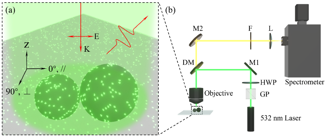
2.1. Sample Fabrication

Silicon nanospheres were fabricated using femtosecond laser ablation of a silicon wafer in deionized (DI) water [27,37,38]. The laser beam passed through the glass tube and ablated silicon surface. After fast cooling in water, the yellow suspension with spherical silicon nanoparticles was collected. We used the femtosecond laser at 1030 nm with a pulse duration of 250 fs and a repetition rate of 1 kHz. The single pulse energy was 700 μJ. Laser pulses were focused by a lens with a focal length of 100 mm. We transferred the silicon nanoparticles from the DI water into ethanol and removed the ultrasmall-sized nanoparticles by centrifugation with 1000 rpm/s for 30 min. Next, in order to obtain nanoparticles with diameters below 200 nm, multi-stage filtering with filter pore sizes of 0.8 μm, 0.45 μm, and 0.22 μm was executed. The yellow suspension became a transparent solution showing the successful filtering of large-scaled particles. After that, the monodispersed silicon nanospheres were spin-coated on a clean glass substrate with an average distribution density of 0.05 μm−2. The silicon dimer was assembled by a commercial atomic force microscope (AFM, Nanowizard II, JPK Instruments, Berlin, Germany) using nanomanipulation mode. The AFM probe in contact mode was controlled to move predetermined particles together. Once the movement was completed, the AFM was switched from the nanomanipulation mode to the image mode, and imaging particles in tapping mode were then used to examine the manipulation result. The steps were repeated until the silicon dimers were tightly compacted against each other. The few-layered R6G membrane was thermally evaporated on the substrate in the vacuum chamber. Thoroughly degassed R6G molecules (bought from Acros Organics, Waltham, MA, USA) in a homemade Knudsen cell were thermally evaporated onto the substrate in a 10−8 mbar vacuum at room temperature. The evaporation rate and the molecular coverage on a gold substrate (Figure 1a) were calibrated several times using a scanning tunneling microscope (STM) at 80 K, which demonstrated that the thickness of one monolayer is about 0.3 nm (Figure 1b). Then, an R6G membrane with a thickness of about four monolayers (~1.2 nm) was sublimated onto the silicon dimer by extending the deposition time appropriately under the same condition (0.8 V, 0.6 A).

2.2. Structural and Optical Characterization

Transmission electron microscope (TEM) images and element analysis were taken on a JEM-2100F microscopy. AFM images were acquired using the tapping mode of 1 Hz scanning speed and a resolution of 2 nm/pixel. The luminescence properties of a few-layered R6G membrane on a silicon dimer at room temperature were studied in a homemade scanning microscope. Figure 2a shows the schematic of the R6G membrane on the silicon dimer excited by a polarized laser. Here, when laser polarization is parallel or perpendicular to the dimer axis, it is defined as longitudinal (0°, //) or transverse (90°, ⊥) excitation. As illustrated in Figure 2b, a continuous-wave laser at 532 nm was used as the excitation source in the homemade scanning microscope. At the output of the laser, a Glan–Taylor prism combined with a half-wave plate was used to control the polarization direction of the excitation. The linear polarized laser was reflected by a dichroic mirror and focused using a microscope objective (×60, N.A. =0.7, LUCPlanFLN, Olympus, Tokyo, Japan) with a focal spot size of ~0.9 μm. The photoluminescence (PL) spectra, after passing through a notch filter to remove the excitation laser, were collected by a spectrometer (SpectraPro-300i, Acton Research Corporation, Acton, MA, USA) for spectrum analysis. The silicon dimers were illuminated by a white light integrated with a condenser (IX-ADUCD, Olympus), and their dark-field scattering signals were collected through the same objective and sent to the same spectrometer to record the scattering spectra.

2.3. Numerical Simulation

Numerical simulations were performed using commercial FDTD software (FDTD Solutions, Lumerical Solution, Inc. Vancouver, BC, Canada). The silicon nanosphere sizes were estimated by AFM images with diameters of 80 nm, 100 nm, 120 nm, and 160 nm. The optical constants of silicon were reported by Palik [39]. The refractive index of the surrounding medium and glass substrate were set at 1.0 and 1.5, respectively. The refractive index of R6G was not considered in the simulation because of the discontinuous coverage of R6G molecules on silicon dimers and possible energy convergence problems in such a thin membrane. A total-field scattered field (TFSF) plane–wave source ranging from 400 to 900 nm was used to illuminate the dimers with longitudinal and transverse polarization. A 3D nonuniform meshing with a grid size of 0.5 nm was applied in the total field domain, with perfectly matched layer (PML) absorption boundary conditions. The scattering cross-section was estimated by calculating the summation of net power flowing into the total and scattered field simulation domains in a set of power monitors. The electric field enhancement maps were collected using the frequency domain field profile monitors. For radiative and nonradiative rate enhancement simulations, a dipole source was located near the gap region, which was 1 nm away from the silicon sphere. Moreover, a quantum efficiency analysis group was placed 300 nm away from the dimers to obtain radiative and nonradiative rate enhancements.

2.4. Multipole Decomposition

The multipole decomposition was accomplished by calculating the displacement current contributions from different multipole moments [40]. When a resonator is illuminated by a plane wave with an electric field amplitude |Ein|= E0 at the frequency f, the induced electric current density J(r) can be expressed as: J ( r ) = i ω ε 0 ( n 2 1 ) E ( r ) , where ω is the angular frequency, ε0 is the permittivity of free space, and n is the refractive indices of the resonator. Under the long-wavelength approximation, the electric dipole p, magnetic dipole m, electric quadrupole Qe, and magnetic quadrupole Qm can be derived using J(r). In addition, the total scattering cross-section can be obtained by the sum of the contributions from different multipole moments [41]:
C sca   total   = C sca p + C sca m + C sca Q e + C sca Q m = k 4 6 π ε 0 2 | E 0 | [ ( | p | 2 + | m c | 2 ) + 1 120 ( | Q e | 2 + | k Q m c | 2 ) + ] ,
where p, m are electric and magnetic dipole moments, respectively, Qe and Qm are the electric and magnetic quadrupole moments, respectively, k is the wavenumber, and 𝑐 is the speed of light.

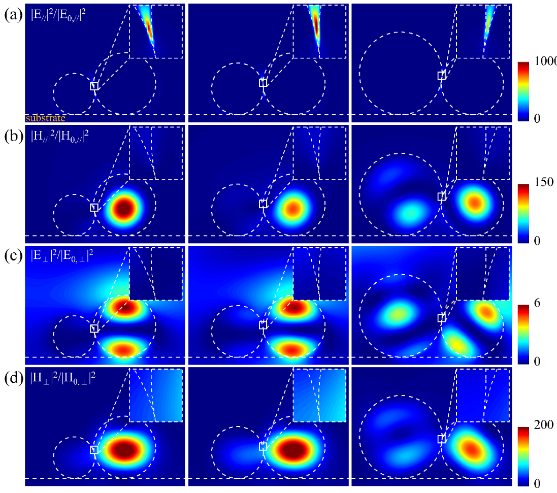
3. Results and Discussion

As depicted in Figure 3a, the representative TEM images of the silicon nanoparticles show great monodispersion and spherical shape with an average diameter of 92 nm. Additionally, the high-resolution TEM image of a silicon nanosphere in Figure 3b indicates that the silicon nanospheres are amorphous. The element analysis shows that the surface of the silicon nanospheres is partly oxidized. Figure 3c shows a typically assembled silicon dimer with nanosphere diameters of about 128.5 nm and 95.9 nm. The diameters of the silicon nanospheres were estimated by extracting the average values from the AFM cross-section analysis. The R6G molecules were thermally evaporated on the substrate in the vacuum chamber, and the thickness of R6G membrane on silicon dimers was approximately 1.2 nm.
To investigate the electric and magnetic enhancement of dimer nanocavity on the PL of R6G membrane, one of the silicon nanospheres with a diameter of approximately 120 nm (D120) was chosen, because of the good resonance overlapping of its magnetic dipolar mode to the excitation laser wavelength. Another one was tuned from 80 nm to 160 nm (D80, D100 and D160). Their measured dark-field scattering spectra are shown in Figure 4a–c. All silicon dimers show an intense resonance at 532 nm. In the dimer of 119.3&77.7, both the electric and magnetic modes of the silicon sphere with a diameter of 77.7 nm are far away from the excitation wavelength. When the diameter of the other silicon sphere is enlarged to 95.9 nm, its magnetic dipolar mode gradually approaches the excitation wavelength. The largest diameter of the silicon sphere is approximately 157.3 nm, and it has a broad electric dipolar mode at the excitation wavelength and can be used to couple with the magnetic resonant mode of the silicon sphere D120. The simulated scattering spectra of three dimers under longitudinal excitation in Figure 4d–f exhibit a great agreement with the experimental results. Additionally, the absorption intensities of all the dimers are much smaller than their scattering intensities.
After four monolayers of R6G molecules were deposited on these three silicon dimers, the laser at 532 nm was used to excite the samples under longitudinal and transverse polarizations. We tried to measure the luminescence for single silicon nanospheres and dimers, but no signal was detected when the same laser power was used to excite the R6G membrane on the dimers. Compared with the PL intensity of the R6G molecules on glass without dimers, the PL of R6G molecules on three dimers are all enhanced. Figure 5a shows the typical PL spectra of the R6G molecules with and without the silicon dimer (128.5&95.9) under longitudinal and transverse excitation, and the enhancement factors of the molecular fluorescence by the three silicon dimers in two polarizations are listed in Table 1. The enhancement factors of the samples under two excitation polarizations are quite small, but the R6G@dimer under longitudinal excitation shows a larger enhancement compared with that under transverse excitation. The enhanced fluorescence of R6G is mainly attributed to the strong scattering ability of the dimers, because of their larger scattering relative to their absorption (Figure 4d–f). This phenomenon expresses the successful formation of silicon nanocavity. In addition, the lifetime of the R6G membrane with and without dimers does not change significantly, and is only slightly prolonged, as shown in Figure 5b. It is known that various plasmonic nanocavities with a strong local enhancement field have been developed and studied, such as hybrid metal-dielectric nanostructures, hybrid plasmonic-photonic systems, and nanoparticle-on-a-mirror configurations, etc. [8,10,42,43]. Compared with these plasmonic nanocavities, the size-mismatched silicon dimer nanocavities have much weaker fluorescence enhancement effects on R6G molecules, which can be attributed to the high fluorescent quenching effect of the R6G molecules adhering to the surface of silicon dimers, which will be discussed below.
To obtain an insight of the mode coupling effect on the excitation of R6G molecules, the near-field profiles of the electric field and magnetic field under longitudinal and transverse light polarization relative to the dimer axis at 532 nm were simulated in Figure 6. Under the longitudinal excitation in Figure 6a, the electric field is extremely compressed in the gap region and produces an electric ‘hot spot’. D120&100 shows the largest electric field enhancement. However, when the incident light is along the transverse direction of the dimer axis, the electric ‘hot spot’ disappeared and there were almost no electric enhancements. This electric polarized property is similar to plasmonic metal dimers and offers a promising route towards efficient controlling in emission. Apart from the electric field enhancement, the magnetic field enhancement in all-dielectric nanostructures is another good candidate for enhancing fluorescence, and the emitter for any orientation can be efficiently excited by the magnetic dipolar resonance due to the circulation of a displacement current [44]. As illustrated in Figure 6b, under longitudinal excitation, the magnetic enhancement is mostly confined inside the silicon sphere with a diameter of 120 nm in D120&100 and D120&80. As for D120&160, high-order magnetic resonance from D160 cannot be neglected, owing to its enhancement for emitters. For the case of transverse excitation in Figure 6c, d, the magnetic dipolar resonance in D120&100 shows the largest enhancement and higher magnetic coupling effectiveness compared to longitudinal excitation and produces a magnetic-type nanocavity. Other dimers exhibit obvious weak interactions, especially for the D120&160. It is well known that the coexistence of electric and magnetic modes can be easily obtained in metal-insulator multilayer nanostructures [4,5,6], and, compared with them, size-mismatched silicon dimers are characterized by the ability to switch the electrical and magnetic mode enhancement in the nanocavities by changing the polarization of the incident light. Combining the scattering spectra in Figure 4 and experimental R6G fluorescence enhancement factors in Table 1, it can be found that, as the size of one silicon nanosphere of dimer gradually increases, when the magnetic modes of two silicon nanospheres can be coupled, the strongest electric and magnetic field enhancements are obtained in the dimer nanocavity. Meanwhile, the dimer nanocavity produces better enhancement of R6G molecules under both longitudinal and transverse polarization excitation.
From Figure 6, it can be found that the electric field enhancement in silicon dimer nanocavities under longitudinal excitation is much stronger than their magnetic field enhancements under transverse excitation. However, the PL enhancement factors of R6G molecules excited along these two polarization directions are not much different (Table 1). To clarify this puzzle and the quenching effect of silicon dimers on R6G fluorescence, the nonradiative and radiative rate enhancements of silicon dimers as a function of emission wavelength under longitudinal and transverse excitation were numerically simulated, as shown in Figure 7. The extremely high nonradiative rate under two excitation polarization directions in Figure 7a,c indicate the strong losses of silicon dimers to R6G fluorescence, which dramatically reduces the fluorescence intensity, leading to a small PL enhancement [45,46]. The radiation rate enhancement of a silicon dimer nanocavity under longitudinal excitation is much stronger than that under transverse excitation (Figure 7b,d). However, the electric mode of dimers is dipolar, and usually the electric dipole mode is radiative, resulting in significant radiation losses. This, coupled with the higher nonradiative rate enhancement of the electric mode relative to the magnetic mode, results in large R6G fluorescence quenching by the electric mode, and little difference in the fluorescence enhancement factors of R6G molecules between the electrical and magnetic modes. To achieve substantial fluorescence enhancement, it is suggested that the nonradiative quadrupole mode of silicon dimers be used [47].
Furthermore, to gain a deeper insight into the different modes’ contributions to the R6G fluorescence enhancement, the multipole decomposition approach is employed in Figure 8 [40]. The exact multipole moments are used to analyze the electric and magnetic dipolar and quadrupole mode contributions to local-field enhancement at 532 nm in dimers. Under the longitudinal excitation, a broadened electric dipolar mode is produced and shows a dominant contribution compared to the suppressed magnetic dipolar mode (Figure 8a–c). The high-order modes in D120&80 and D120&100 have little contribution and can be ignored, but the electric quadrupole in D120&160 shows a considerable enhancement at the excitation wavelength. As for transverse excitation, the electric coupling between the two silicon nanospheres in D120&100 and D120&80 is very weak, and a suppressed electric dipolar mode is obtained in D120&160 (Figure 8d–f). However, the magnetic dipolar mode is dominant, and the high-order magnetic mode becomes a considerable enhancement element at 532 nm. Due to the fact that the electric mode of D160 is resonant with excitation, the electric enhancement and the magnetic enhancement show a comparable strength. Consequently, under longitudinal excitation, the dimer exhibits a nanoscale nanocavity and the electric mode shows a stronger enhancement compared with the magnetic mode. While under transverse excitation, the primary enhancement originates from the magnetic mode.

4. Conclusions

Size-mismatched silicon dimer nanocavities were constructed and interacted with a R6G membrane to investigate the enhancement of electric and magnetic-mode coupling. The R6G fluorescence under both longitudinal excitation and transverse excitation exhibits a stronger enhancement compared with that without silicon dimers. Additionally, the lifetime of a nanocavity coupled R6G is slightly prolonged. These pieces of evidence express the successful formation of nanocavities. The simulated electric and magnetic field distributions and decomposed mode of nanocavity show primary electric mode enhancement under longitudinal excitation and dominate magnetic mode enhancement under transverse excitation. Such a silicon dimer is a promising nanocavity with flexible interaction and electric and magnetic mode enhancement and can be used in sensing and all-dielectric metamaterials or nanophotonic devices.

Author Contributions

Conceptualization, C.P. and Y.B.; methodology, C.P. and Y.B.; software, B.W.; validation, X.Z., B.W. and Q.J.; formal analysis, C.P.; investigation, C.P. and Y.B.; resources, X.Z. and B.W.; data curation, C.P., Y.B., Y.Z. and S.Z.; writing–original draft preparation, C.P. and Y.B.; writing–review and editing, X.Z. and B.W.; supervision, X.Z. and B.W.; project administration, X.Z., B.W., Q.J. and E.W.; funding acquisition, X.Z., B.W., Q.J. and E.W. All authors have read and agreed to the published version of the manuscript.

Funding

This research was funded by the National Key Research and Development Program of China (2021YFA1201503, 2017YFA0303403), the Natural Science Foundation of Shanghai (22ZR1421100), the National Natural Science Foundation of China (11874015, 12074072, 11621404), the Program of Introducing Talents of Discipline to Universities (B12024), the Natural Science Foundation Project of CQ CSTC2021JCYJ-MAXMX0356, and the Research Funds of Happiness Flower ECNU (2021ST2110).

Institutional Review Board Statement

Not applicable.

Informed Consent Statement

Not applicable.

Data Availability Statement

Data used in the text and MATLAB codes are available from corresponding authors with reasonable request.

Acknowledgments

The authors appreciate the reviewers taking time to read this manuscript and to give helpful suggestions for further improvement.

Conflicts of Interest

The authors declare no conflict of interest.

References

  1. May, M.A.; Fialkow, D.; Wu, T.; Park, K.; Leng, H.; Kropp, J.A.; Gougousi, T.; Lalanne, P.; Pelton, M.; Raschke, M.B. Nano-Cavity QED with Tunable Nano-Tip Interaction. Adv. Quantum Technol. 2020, 3, 1900087. [Google Scholar] [CrossRef]
  2. Juraschek, D.M.; Neuman, T.; Flick, J.; Narang, P. Cavity Control of Nonlinear Phononics. Phys. Rev. Res. 2021, 3, L032046. [Google Scholar] [CrossRef]
  3. Verre, R.; Maccaferri, N.; Fleischer, K.; Svedendahl, M.; Odebo Länk, N.; Dmitriev, A.; Vavassori, P.; Shvets, I.V.; Käll, M. Polarization Conversion-Based Molecular Sensing Using Anisotropic Plasmonic Metasurfaces. Nanoscale 2016, 8, 10576–10581. [Google Scholar] [CrossRef] [PubMed]
  4. Frederiksen, M.; Bochenkov, V.E.; Ogaki, R.; Sutherland, D.S. Onset of Bonding Plasmon Hybridization Preceded by Gap Modes in Dielectric Splitting of Metal Disks. Nano Lett. 2013, 13, 6033–6039. [Google Scholar] [CrossRef] [PubMed]
  5. Maccaferri, N.; Zhao, Y.; Isoniemi, T.; Iarossi, M.; Parracino, A.; Strangi, G.; De Angelis, F. Hyperbolic Meta-Antennas Enable Full Control of Scattering and Absorption of Light. Nano Lett. 2019, 19, 1851–1859. [Google Scholar] [CrossRef]
  6. Verre, R.; Yang, Z.J.; Shegai, T.; Käll, M. Optical Magnetism and Plasmonic Fano Resonances in Metal-Insulator-Metal Oligomers. Nano Lett. 2015, 15, 1952–1958. [Google Scholar] [CrossRef]
  7. Ardini, M.; Huang, J.-A.; Sánchez, C.S.; Mousavi, M.Z.; Caprettini, V.; Maccaferri, N.; Melle, G.; Bruno, G.; Pasquale, L.; Garoli, D.; et al. Live Intracellular Biorthogonal Imaging by Surface Enhanced Raman Spectroscopy Using Alkyne-Silver Nanoparticles Clusters. Sci. Rep. 2018, 8, 12652. [Google Scholar] [CrossRef]
  8. Barreda, A.I.; Zapata-Herrera, M.; Palstra, I.M.; Mercadé, L.; Aizpurua, J.; Koenderink, A.F.; Martínez, A. Hybrid Photonic-Plasmonic Cavities Based on the Nanoparticle-on-a-Mirror Configuration. Photonics Res. 2021, 9, 2398. [Google Scholar] [CrossRef]
  9. Kuznetsov, A.I.; Miroshnichenko, A.E.; Brongersma, M.L.; Kivshar, Y.S.; Luk’yanchuk, B. Optically Resonant Dielectric Nanostructures. Science. 2016, 354, aag2472. [Google Scholar] [CrossRef] [Green Version]
  10. Barreda, Á.; Vitale, F.; Minovich, A.E.; Ronning, C.; Staude, I. Applications of Hybrid Metal-Dielectric Nanostructures: State of the Art. Adv. Photonics Res. 2021, 2100286. [Google Scholar] [CrossRef]
  11. Jahani, S.; Jacob, Z. All-Dielectric Metamaterials. Nat. Nanotechnol. 2016, 11, 23–36. [Google Scholar] [CrossRef] [PubMed]
  12. Albella, P.; Poyli, M.A.; Schmidt, M.K.; Maier, S.A.; Moreno, F.; Sáenz, J.J.; Aizpurua, J. Low-Loss Electric and Magnetic Field-Enhanced Spectroscopy with Subwavelength Silicon Dimers. J. Phys. Chem. C 2013, 117, 13573–13584. [Google Scholar] [CrossRef] [Green Version]
  13. Bakker, R.M.; Permyakov, D.; Yu, Y.F.; Markovich, D.; Paniagua-Domínguez, R.; Gonzaga, L.; Samusev, A.; Kivshar, Y.; Luk’yanchuk, B.; Kuznetsov, A.I. Magnetic and Electric Hotspots with Silicon Nanodimers. Nano Lett. 2015, 15, 2137–2142. [Google Scholar] [CrossRef] [PubMed]
  14. Razdolski, I.; Chen, Y.; Giles, A.J.; Gewinner, S.; Schöllkopf, W.; Hong, M.; Wolf, M.; Giannini, V.; Caldwell, J.D.; Maier, S.A.; et al. Resonant Enhancement of Second-Harmonic Generation in the Mid-Infrared Using Localized Surface Phonon Polaritons in Subdiffractional Nanostructures. Nano Lett. 2016, 16, 6954–6959. [Google Scholar] [CrossRef] [PubMed]
  15. Kilic, U.; Hilfiker, M.; Ruder, A.; Feder, R.; Schubert, E.; Schubert, M.; Argyropoulos, C. Broadband Enhanced Chirality with Tunable Response in Hybrid Plasmonic Helical Metamaterials. Adv. Funct. Mater. 2021, 31, 2010329. [Google Scholar] [CrossRef]
  16. Krasnok, A.E.; Miroshnichenko, A.E.; Belov, P.A.; Kivshar, Y.S. All-Dielectric Optical Nanoantennas. Opt. Express 2012, 20, 20599. [Google Scholar] [CrossRef]
  17. Schmidt, M.K.; Esteban, R.; Sáenz, J.J.; Suárez-Lacalle, I.; Mackowski, S.; Aizpurua, J. Dielectric Antennas—A Suitable Platform for Controlling Magnetic Dipolar Emission: Errata. Opt. Express 2012, 20, 18609. [Google Scholar] [CrossRef]
  18. Koshelev, K.; Kivshar, Y. Dielectric Resonant Metaphotonics. ACS Photonics 2021, 8, 102–112. [Google Scholar] [CrossRef]
  19. Genevet, P.; Capasso, F.; Aieta, F.; Khorasaninejad, M.; Devlin, R. Recent Advances in Planar Optics: From Plasmonic to Dielectric Metasurfaces. Optica 2017, 4, 139. [Google Scholar] [CrossRef]
  20. Xiang, J.; Chen, J.; Lan, S.; Miroshnichenko, A.E. Nanoscale Optical Display and Sensing Based on the Modification of Fano Lineshape. Adv. Opt. Mater. 2020, 8, 2000489. [Google Scholar] [CrossRef]
  21. Liu, T.; Xu, R.; Yu, P.; Wang, Z.; Takahara, J. Multipole and Multimode Engineering in Mie Resonance-Based Metastructures. Nanophotonics 2020, 9, 1115–1137. [Google Scholar] [CrossRef]
  22. Maimaiti, A.; Patra, P.P.; Jones, S.; Antosiewicz, T.J.; Verre, R. Low-Loss Hybrid High-Index Dielectric Particles on a Mirror for Extreme Light Confinement. Adv. Opt. Mater. 2020, 8, 1901820. [Google Scholar] [CrossRef]
  23. Xu, J.; Wu, Y.; Zhang, P.; Wu, Y.; Vallée, R.A.L.; Wu, S.; Liu, X. Resonant Scattering Manipulation of Dielectric Nanoparticles. Adv. Opt. Mater. 2021, 9, 2100112. [Google Scholar] [CrossRef]
  24. Kuznetsov, A.I.; Miroshnichenko, A.E.; Fu, Y.H.; Zhang, J.; Luk’yanchuk, B. Magnetic Light. Sci. Rep. 2012, 2, 492. [Google Scholar] [CrossRef] [PubMed] [Green Version]
  25. Xiao, H.; Wu, X.; Liu, Z.; Zhao, G.; Guo, X.; Meng, Y.; Deng, L.; Chen, W.; Tian, Y.; Yang, J. Tunable Fano Resonance in Mutually Coupled Micro-Ring Resonators. Appl. Phys. Lett. 2017, 111, 091901. [Google Scholar] [CrossRef]
  26. Wang, H.; Ke, Y.; Xu, N.; Zhan, R.; Zheng, Z.; Wen, J.; Yan, J.; Liu, P.; Chen, J.; She, J.; et al. Resonance Coupling in Silicon Nanosphere-J-Aggregate Heterostructures. Nano Lett. 2016, 16, 6886–6895. [Google Scholar] [CrossRef] [PubMed]
  27. Wang, H.; Wen, J.; Wang, W.; Xu, N.; Liu, P.; Yan, J.; Chen, H.; Deng, S. Resonance Coupling in Heterostructures Composed of Silicon Nanosphere and Monolayer WS2: A Magnetic-Dipole-Mediated Energy Transfer Process. ACS Nano 2019, 13, 1739–1750. [Google Scholar] [CrossRef]
  28. Yan, J.; Liu, P.; Lin, Z.; Wang, H.; Chen, H.; Wang, C.; Yang, G. Directional Fano Resonance in a Silicon Nanosphere Dimer. ACS Nano 2015, 9, 2968–2980. [Google Scholar] [CrossRef]
  29. Miroshnichenko, A.E.; Evlyukhin, A.B.; Kivshar, Y.S.; Chichkov, B.N. Substrate-Induced Resonant Magnetoelectric Effects for Dielectric Nanoparticles. ACS Photonics 2015, 2, 1423–1428. [Google Scholar] [CrossRef]
  30. Wang, Z.; Chen, M.; Zhang, W. Sub-50 nm Control of Light at 405 Nm with Planar Si Nanolens. Opt. Express 2022, 30, 9904. [Google Scholar] [CrossRef]
  31. Zywietz, U.; Schmidt, M.K.; Evlyukhin, A.B.; Reinhardt, C.; Aizpurua, J.; Chichkov, B.N. Electromagnetic Resonances of Silicon Nanoparticle Dimers in the Visible. ACS Photonics 2015, 2, 913–920. [Google Scholar] [CrossRef] [Green Version]
  32. Caldarola, M.; Albella, P.; Cortés, E.; Rahmani, M.; Roschuk, T.; Grinblat, G.; Oulton, R.F.; Bragas, A.V.; Maier, S.A. Non-Plasmonic Nanoantennas for Surface Enhanced Spectroscopies with Ultra-Low Heat Conversion. Nat. Commun. 2015, 6, 7915. [Google Scholar] [CrossRef] [PubMed] [Green Version]
  33. Regmi, R.; Berthelot, J.; Winkler, P.M.; Mivelle, M.; Proust, J.; Bedu, F.; Ozerov, I.; Begou, T.; Lumeau, J.; Rigneault, H.; et al. All-Dielectric Silicon Nanogap Antennas to Enhance the Fluorescence of Single Molecules. Nano Lett. 2016, 16, 5143–5151. [Google Scholar] [CrossRef] [PubMed] [Green Version]
  34. Bian, Y.; Liu, S.; Zhang, Y.; Liu, Y.; Yang, X.; Lou, S.; Wu, E.; Wu, B.; Zhang, X.; Jin, Q. Distance-Dependent Plasmon-Enhanced Fluorescence of Submonolayer Rhodamine 6G by Gold Nanoparticles. Nanoscale Res. Lett. 2021, 16, 90. [Google Scholar] [CrossRef] [PubMed]
  35. Hu, F.; Gao, S.; Zhu, L.; Liao, F.; Yang, L.; Shao, M. Tunable Fluorescence Enhancement Based on Bandgap-Adjustable 3D Fe3O4 Nanoparticles. Nanotechnology 2016, 27, 245709. [Google Scholar] [CrossRef] [PubMed]
  36. Roy, S.; Sharbirin, A.S.; Lee, Y.; Kim, W.B.; Kim, T.S.; Cho, K.; Kang, K.; Jung, H.S.; Kim, J. Measurement of Quantum Yields of Monolayer TMDs Using Dye-Dispersed PMMA Thin Films. Nanomaterials 2020, 10, 1032. [Google Scholar] [CrossRef]
  37. Fu, Y.H.; Kuznetsov, A.I.; Miroshnichenko, A.E.; Yu, Y.F.; Luk’yanchuk, B. Directional Visible Light Scattering by Silicon Nanoparticles. Nat. Commun. 2013, 4, 1527. [Google Scholar] [CrossRef] [Green Version]
  38. Zywietz, U.; Evlyukhin, A.B.; Reinhardt, C.; Chichkov, B.N. Laser Printing of Silicon Nanoparticles with Resonant Optical Electric and Magnetic Responses. Nat. Commun. 2014, 5, 3402. [Google Scholar] [CrossRef]
  39. Palik, E.D. Handbook of Optical Constants of Solids; Academic Press: Cambridge, MA, USA, 1998. [Google Scholar]
  40. Alaee, R.; Rockstuhl, C.; Fernandez-Corbaton, I. An Electromagnetic Multipole Expansion beyond the Long-Wavelength Approximation. Opt. Commun. 2018, 407, 17–21. [Google Scholar] [CrossRef] [Green Version]
  41. Jackson, J.D. Classical Electrodynamics, 3rd ed.; Wiley: Hoboken, NJ, USA, 1998. [Google Scholar]
  42. Akselrod, G.M.; Argyropoulos, C.; Hoang, T.B.; Ciracì, C.; Fang, C.; Huang, J.; Smith, D.R.; Mikkelsen, M.H. Probing the Mechanisms of Large Purcell Enhancement in Plasmonic Nanoantennas. Nat. Photonics 2014, 8, 835–840. [Google Scholar] [CrossRef] [Green Version]
  43. Benz, F.; Schmidt, M.K.; Dreismann, A.; Chikkaraddy, R.; Zhang, Y.; Demetriadou, A.; Carnegie, C.; Ohadi, H.; Nijs, B.D.; Esteban, R.; et al. Single-Molecule Optomechanics in “Picocavities”. Science 2016, 354, 726–729. [Google Scholar] [CrossRef] [PubMed] [Green Version]
  44. Stamatopoulou, P.E.; Tserkezis, C. Role of Emitter Position and Orientation on Silicon Nanoparticle-Enhanced Fluorescence. OSA Contin. 2021, 4, 918. [Google Scholar] [CrossRef]
  45. Delga, A.; Feist, J.; Bravo-Abad, J.; Garcia-Vidal, F.J. Quantum Emitters Near a Metal Nanoparticle: Strong Coupling and Quenching. Phys. Rev. Lett. 2014, 112, 253601. [Google Scholar] [CrossRef] [PubMed]
  46. Kongsuwan, N.; Demetriadou, A.; Chikkaraddy, R.; Benz, F.; Turek, V.A.; Keyser, U.F.; Baumberg, J.J.; Hess, O. Suppressed Quenching and Strong-Coupling of Purcell-Enhanced Single-Molecule Emission in Plasmonic Nanocavities. ACS Photonics 2018, 5, 186–191. [Google Scholar] [CrossRef] [Green Version]
  47. Sugimoto, H.; Fujii, M. Magnetic Purcell Enhancement by Magnetic Quadrupole Resonance of Dielectric Nanosphere Antenna. ACS Photonics 2021, 8, 1794–1800. [Google Scholar] [CrossRef]
Figure 1. (a) STM image of monolayer R6G. The blue line marks the location of the cross-section analysis. (b) Corresponding cross-section analysis result for line in (a).
Photonics 09 00267 g001
Figure 2. (a) Schematic of silicon dimer excited by a continuous-wave laser at 532 nm with controlled polarization. The straight arrows indicate the direction and polarization of the incident laser, and the curved arrow indicates the emission of R6G. (b) Schematic of the experimental setup. A homemade scanning microscope was used. GP: Glan prism, HWP: half-wave plate, M: silver mirror, DM: dichroic mirror, F: filter, L: lens.
Photonics 09 00267 g002
Figure 3. (a) TEM image of silicon nanospheres with an average diameter of 92 nm. (b) High-resolution TEM image of a silicon nanosphere. (c) Typical AFM topographic image of the silicon dimer with diameters of about 128.5 nm and 95.9 nm and corresponding cross-section analysis along the longitudinal axis of silicon dimer.
Photonics 09 00267 g003
Figure 4. (ac) The experimental dark-field scattering spectra of three silicon dimers. Inset: AFM topographic images of the silicon dimers and corresponding diameters. Scale bar: 100 nm. (df) The simulated scattering and absorption spectra of the corresponding nanostructures under longitudinal excitation and related dimers in simulation.
Photonics 09 00267 g004
Figure 5. (a) Typical PL spectra of the R6G molecules with and without the silicon dimer under longitudinal and transverse excitation. (b) Decay curves of R6G@dimers under longitudinally polarized laser excitation.
Photonics 09 00267 g005
Figure 6. Simulated electric and magnetic field enhancement distributions of silicon dimers under (a,b) longitudinal and (c,d) transverse excitation at 532 nm.
Photonics 09 00267 g006
Figure 7. (a,c) nonradiative and (b,d) radiative rate enhancements of silicon dimers as a function of emission wavelength under longitudinal and transverse excitation.
Photonics 09 00267 g007
Figure 8. Simulated light-scattering spectra with mode decomposition under (ac) longitudinal excitation and (df) transverse excitation. (a,d) D120&80, (b,e) D120&&100, (c,f) D120&160. ED: electric dipole; MD: magnetic dipole; EQ: electric quadrupole; MQ: magnetic quadrupole.
Photonics 09 00267 g008
Table 1. Enhancement Factors of R6G@Dimers under Longitudinally and Transversely Polarized Laser Excitation.
SampleEnhancement Factors
//
R6G@119.3&77.72.461.02
R6G@128.5&95.92.091.58
R6G@123.9&157.32.321.21
Publisher’s Note: MDPI stays neutral with regard to jurisdictional claims in published maps and institutional affiliations.

