Communication

Tunable Triple Plasmonically Induced Transparency in Triangular Cavities Coupled with an MDM Waveguide

1
School of Electronic Engineering, Heilongjiang University, Harbin 150080, China
2
Heilongjiang Provincial Key Laboratory of Metamaterials Physics and Device, Heilongjiang University, Harbin 150080, China
*
Author to whom correspondence should be addressed.
Photonics 2022, 9(2), 100; https://doi.org/10.3390/photonics9020100
Submission received: 10 January 2022 / Revised: 27 January 2022 / Accepted: 6 February 2022 / Published: 9 February 2022

Abstract

:
In this paper, a side-coupled triangle cavity in a plasmonic waveguide structure is proposed and numerically analyzed by the finite-difference time-domain (FDTD) method and coupled mode theory (CMT). Triple plasmonically induced transparency (PIT) was achieved when an extra triangle was added into the structure, and the transmission characteristics were investigated. This novel structure has a maximal sensitivity of 933 nm/RIU when used as a sensor and a contrast ratio of 4 dB. Moreover, the tunability of PIT can be realized by filling the nematic liquid crystal (NLC) E7 into the triangles. The refractive index of E7 changes with the applied electric field. Given that E7 is also sensitive to temperature, this structure can be used as a temperature sensor with a sensitivity of 0.29 nm/°C. It is believed that this tunable structure with PIT may have potential applications in highly integrated optical circuits.

1. Introduction

Surface plasmon polaritons (SPPs), as special electromagnetic evanescent waves, propagate along the metal–dielectric interface and exponentially attenuate perpendicular to the interface [1]. SPPs are considered to be the most promising information carriers owing to their advantages, such as manipulating light at the nanoscale and overcoming the classical limit [2]. With many advantages, SPPs are widely used in optical communication and biochemical sensing [3]. Huifang Ai et al. devised a metasurface which realizes multi-beam steering to meet the demand of indoor directional 6G communications [4]. Fatemeh et al. designed a multifunctional sensor which can be used to detect various biological analytes with ultra-low concentrations [5]. Furthermore, using an analogous strategy, Xie et al. proposed a plasmonic metasurface consisting of a series of arrays on a silicon substrate, in order to detect the changes in kanamycin sulfate amounts at a relatively low concentration [6]. Lee and coworkers studied a highly sensitive and tunable method to detect the decrease in carbohydrate molecules with a sensing THz metasurface based on nanoantennas. They stated that the metasurface was able to recognize different carbohydrate molecules even at very low concentrations [7].
There are many different methods which can be used to excite SPPs. Prisms in the Turbadar–Kretschmann–Raether structure and the Turbadar–Otto structure are employed to excite SPPs [8]. Furthermore, the excitation of SPPs can be accomplished using a parallel waveguide [9], a coupler [10], or a grating [11], although these methods suffer from low efficiency when transferring free-space radiation energy to the SPP. As for metal–dielectric–metal (MDM) waveguides, they are widely used in optical devices as a result of their capabilities, such as strong light confinement, high efficiency, and easy fabrication [12].
The electromagnetically induced transparency (EIT) effect, a narrow transparency window in the absorption band observed in atomic media [13], provides a solution for devices in slow light and data storage [14]. However, because the application of EIT is limited by extreme experimental conditions [15], plasmonically induced transparency (PIT) is preferable as it can be easily realized in plasmonic structures [16]. In fact, PIT is an analogous phenomenon to EIT which manifests as a sharp peak in the intrinsic band-stop filtering transmission dip. Thus, PIT attracts a significant amount of attention and can be achieved in many different plasmonic structures, e.g., graphene nanostrips [17], MDM waveguides [18], and metamaterials [19]. Among these structures, various PIT devices based on an MDM waveguide have been proposed such as optical switches [20], sensors [21], and filters [22]. In addition, the tunability of PIT is mostly realized by employing graphene, whose permittivity varies depending on the applied voltage [23,24]. However, although graphene can conduct electricity, its unstable conductivity cannot be ignored, and it can only be used in combination with other substances which are also unstable when exposed to air and water [25]. Furthermore, graphene is not sensitive to changes in temperature, and sensing applications based on PIT are seldom focused on temperature sensing [26].
Nematic liquid crystals (NLCs) consist of rod-like molecules that are aligned parallel to a specific angle in space. Therefore, NLCs show strong electrical and optical anisotropy. The extraordinary refractive index along the molecule axis is much higher than the ordinary refractive index. The structure of NLCs leads to large and controllable birefringence [23], which shows great advantages, including reliability and low power consumption. Moreover, NLC components are designed into polarization rotators, switches, sensors, etc. [24,27].
In this work, we realized triple PIT based on two triangles coupled with an MDM waveguide. With a liquid crystal added, tunability and high sensitivity towards the temperature change of the triple PIT were achieved. Firstly, a simple plasmonic structure is proposed, consisting of a triangular cavity and an MDM waveguide. The transmission characteristics of the structure were analyzed by the finite-difference time-domain (FDTD) method and coupled mode theory (CMT). Another triangular cavity was added into the structure to realize a PIT effect. The transmission spectra can be adjusted by changing the geometrical parameters of the topological structure, which provides a good sensitivity ( S ) of 933 nm/RIU and a contrast ratio ( C R ) of 4 dB. In addition, when NLC E7 is added into the triangular cavities, the transparency window can be manipulated by the director angle of E7. Furthermore, this structure can be employed as a temperature sensor with a sensitivity of 0.29 nm/°C because E7 is sensitive to temperature change. It is believed that this compact structure with tunable PIT can be used in other plasmonic devices.

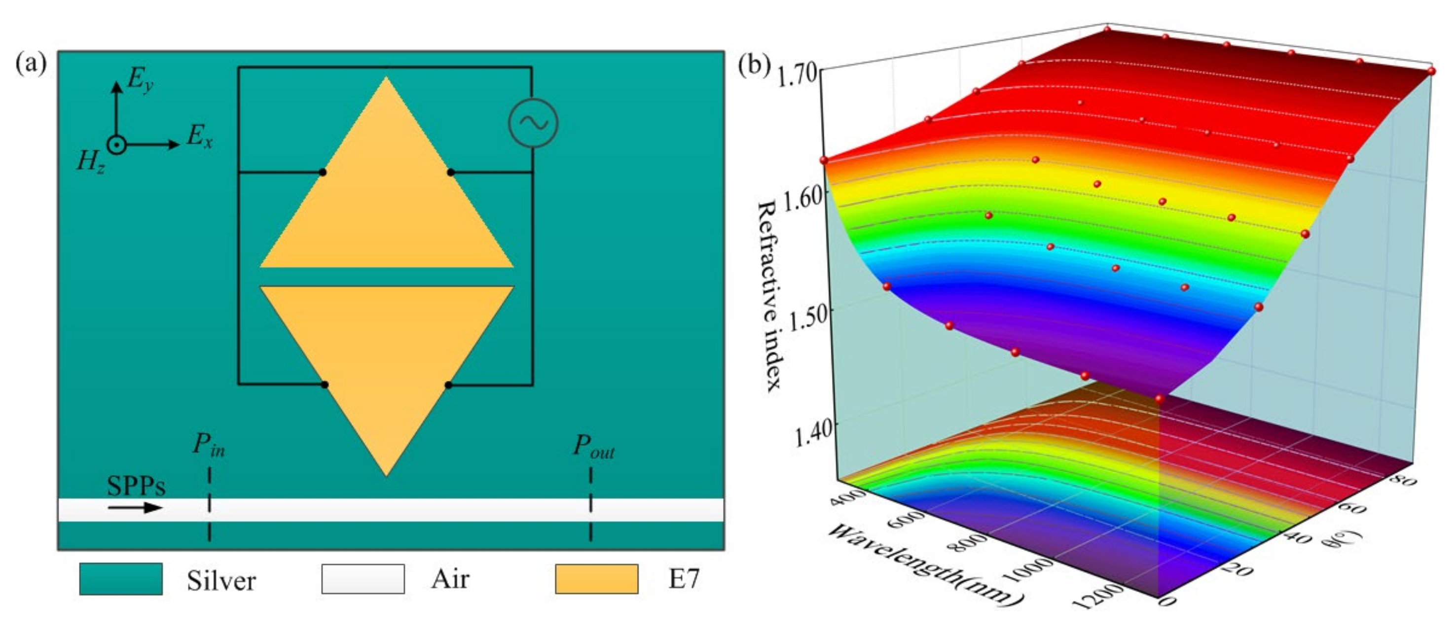
2. Materials and Methods

Figure 1a illustrates the three-dimensional schematic of the proposed MDM waveguide structure. The structure can be etched on a silver surface deposited on a silicon substrate. The equilateral triangular side length is L = 484 nm, and the distance between the triangle and the waveguide is D1 = 30 nm. The width of the waveguide (W) is 50 nm, which ensures that the waveguide only supports the fundamental mode [28,29].
In the simulation, calculated by the Lumerical FDTD Solutions software 8.15.736, the three-dimensional model was substituted with a two-dimensional model to dramatically decrease the computational time. Four perfectly matched layers were used to absorb the escaping energy of the structure with minimal reflection. Johnson and Christy’s model [30] was chosen to describe the optical characteristics of the silver.
The dispersion relation of the fundamental mode in the MDM waveguide can be written as [31,32]
β 2 ε m k 0 2 / ε m β 2 ε d k 0 2 / ε d = tanh ( L β 2 ε d k 0 2 2 )
where β is the propagation constant, ε m is the permittivity of the metal, ε d is the dielectric permittivity, and k 0 is the wave vector. The resonance wavelengths λ r of the structure can be obtained from the following equation:
λ r = 3 L e f f β / k 0 α ψ / 2 π
where α is an integer, L e f f is the effective length of the triangle, equal to the height of the triangle, and ψ = 0 is the total phase shift when the light is coupled into the triangle and back to the waveguide. Combining Equations (1) and (2), λ r can be obtained at 506 nm, 598 nm, and 936 nm, which are consistent with the resonance wavelengths calculated by FDTD in Figure 1b.
CMT was also used to illustrate the transmission spectra of the structure in Figure 1b. The amplitudes of the input and output lights are expressed as S 11 + , S 11 , S 12 + , S 12 , S 21 + , and S 21 , which are shown in Figure 1a. When light with an angular frequency ω is injected into the structure ( S 12 + = 0), the time evolution of the amplitude a q ( q = 1, 2, and 3) can be represented as follows:
d a q d t = ( j w q 1 / τ c q 1 / τ i q ) a q + 1 / τ c q S 11 + exp ( j θ 1 ) + 2 / τ i q S 21 + exp ( j θ 2 )
S 21 + = δ S 21 exp ( j φ )
S 12 = S 11 + a q 1 / τ c q exp ( j θ 1 )
S 21 = S 21 + + a q 2 / τ i q exp ( j θ 2 )
Here, j is the imaginary part ( j 2 = 1 ) and ω q denotes the resonance angular frequency of the structure. τ c q is the decay time due to light escaping into the waveguide, and τ i q is the decay time because of the triangular intrinsic loss. These two parameters satisfy 1 / τ c q = ω q / 2 Q c q and 1 / τ i q = ω q / 2 Q i q , respectively. The phase of the coupling coefficient is expressed as θ i ( i = 1, 2). δ and φ denote the amplitude attenuation and phase shift between input and output lights.
Combining Equations (3)–(6), the transmittance can be deduced as
T ( w ) = S 12 S 11 + 2 = j ( w q w ) + ( 1 / τ i q ) 1 δ exp ( j φ ) / 1 + δ exp ( j φ ) j ( w q w ) + ( 1 / τ c q ) + ( 1 / τ i q ) 1 δ exp ( j φ ) / 1 + δ exp ( j φ ) 2
φ ( w ) = w n e f f L e f f / c + θ
Here, θ = 0 expresses the additional phase change of the MDM waveguide [33,34]. The result obtained by CMT is depicted in Figure 1b by the red dotted line. The result has the same tendency as the result of FDTD. The values of the parameters are w 1 = 3.72 × 10¹⁵ rad/s, w 2 = 3.15 × 10¹⁵ rad/s, w 3 = 2.01 × 10¹⁵ rad/s, τ c 1 = 0.33 ps, τ i 1 = 0.21 ps, τ c 2 = 0.85 ps, τ i 2 = 0.21 ps, τ c 3 = 0.20 ps, τ i 3 = 0.23 ps, and δ = 0.971.

3. Results and Discussion

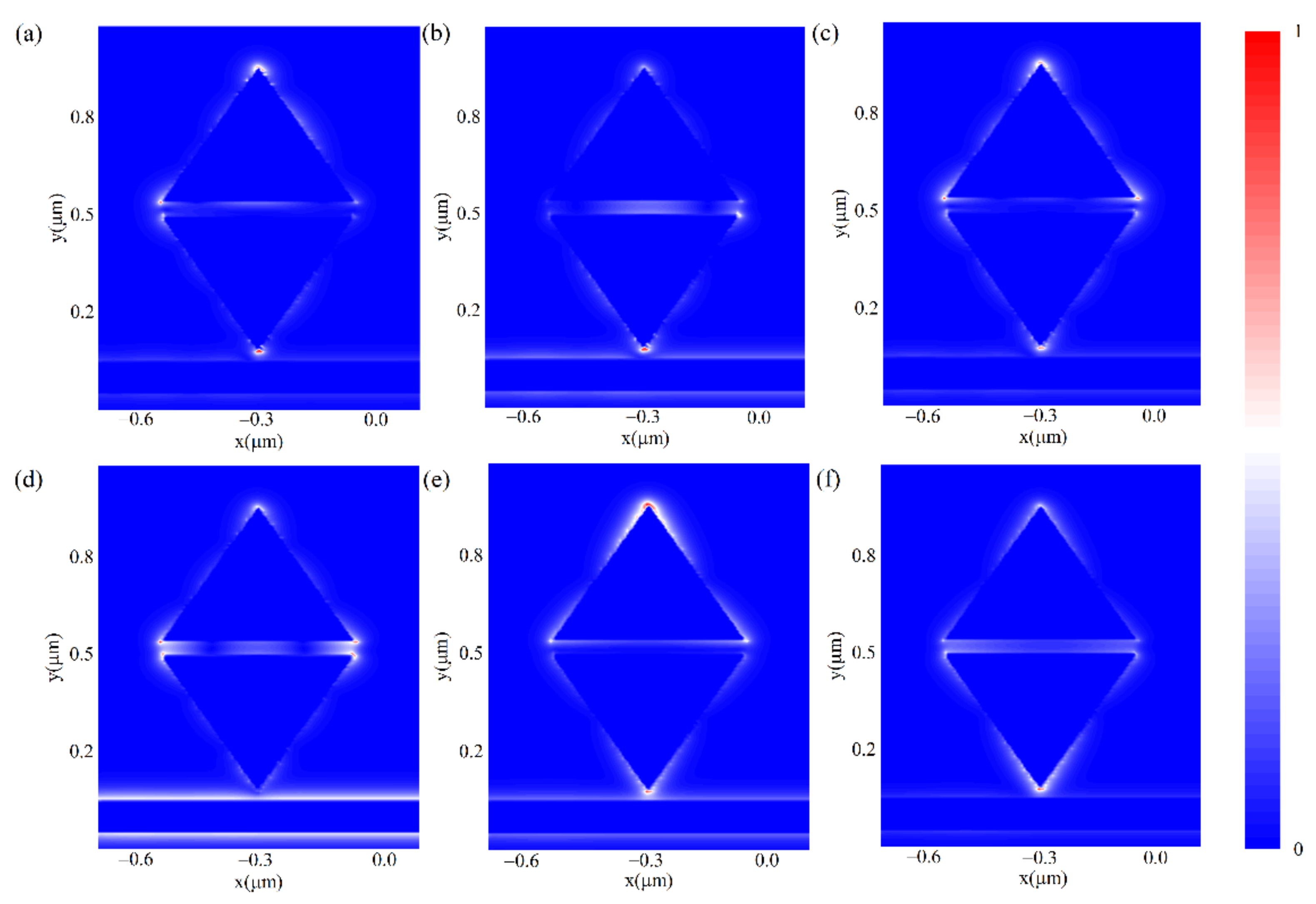
3.1. Theoretical Analysis of Structure

In Figure 2a, the transmission spectra of the structure are changed by varying L. The resonance wavelength at each dip of the structure has a redshift when L changes from 435.6 nm to 508.2 nm. Moreover, the transmittance shows an obvious decrease from 435.6 nm to 459.8 nm, whereas the transmittance has a slight change from 459.8 nm to 508.2 nm. L = 484 nm was chosen due to the slight change in transmittance and the regular change in the resonance wavelengths from 459.8 nm to 508.2 nm, in order to obtain a relatively high fault tolerance in real manufacturing [35]. Figure 2b illustrates the influence on transmission spectra with different D1 values. With an increase in D1 from 10 nm to 40 nm, the transmittance at each dip reduces with a slight blueshift in each resonance wavelength.

3.2. Theoretical Design of PIT

The configuration of the MDM waveguide structure coupled with triangles is shown in Figure 3a. The geometric parameters of the two triangles are the same. The distance between the two triangles (D2) is 40 nm, and the distance between the inverted triangle and the waveguide is 30 nm. The transmittance of the structure is expressed as T = P o u t / P i n . To highlight the transmission characteristics of PIT, the transmission spectra with/without the upper triangle are depicted in Figure 3b. Three dips at the resonance wavelengths in Figure 1b are replaced by peaks when the upper triangle is introduced, accompanied by the emergence of six sharp absorption dips.
Three-level atomic theory is introduced to explain the mechanism of the PIT effect. The waveguide, the radiant inverted triangle with a bright mode, and the subradiant upper triangle with a dark mode serve as the ground state |1>, excited state |2>, and metastable state |3>, respectively. The PIT effect is formed owing to the destructive interference between two pathways (|1>→|2>→|3>→|2> and |1>→|2>). The first PIT, related to the positions H1, I1, J1, and K1, is formed by the destructive interference between the first pathway, in which light propagates from the waveguide to the inverted triangle and escapes into the upper triangle and back to the inverted one, and the second pathway, in which light is injected into the inverted triangle and is not coupled into the upper triangle. The magnetic field distribution of the first PIT is shown in Figure 4a–d. Figure 4a,c show that energy mainly exists in the vertices of the two triangles. Figure 4b denotes that a small amount of energy exists in the vertex of the upper triangle, and most passes through the waveguide. Figure 4d shows that energy concentrates on the vertex of the inverted triangle. As for the second PIT, similar destructive interference occurs, related to the positions H2, I2, J2, and K2. Figure 4e,g demonstrate that the energy is trapped at the corners of the two triangles. A small amount of energy exists at the corners of the upper triangle, and most propagates through the waveguide in Figure 4f, while energy is found in the corners of the inverted triangle in Figure 4h. For the third PIT, interference is related to positions H3, I3, J3, and K3. Figure 4i,k show that strong energy stays in the vertices of the two triangles. Figure 4j displays strong energy concentrating in the vertex of the upper triangle and the waveguide. Finally, Figure 4l shows that strong energy is found at the vertex of the inverted triangle. Three destructive interferences happen at different positions with different magnetic field distributions to form the triple PIT phenomenon.
Additionally, the current densities are calculated in Figure 5a–f corresponding to the six dips shown in Figure 3b. In Figure 5a,b, current densities are relatively high in the vertices of the two triangles. Moreover, currents mainly concentrate in all of the corners of the two triangles in Figure 5c,d, while currents exist in the vertices of the two triangles in Figure 5e,f.
Subsequently, in Figure 6a, the adjustment of PIT is studied by varying D1 without any other changes to the geometric parameters in Figure 3a. The transmittance at each dip of PIT increases when D1 changes from 40 nm to 10 nm, but the resonance wavelengths of dips are unchanged. Figure 6b displays the effects on transmission spectra with different D2 values. With an increase in D2 from 20 nm to 50 nm, each transparency window of PIT reduces.
PIT can be used as an all-optical switch which is essential in the design of highly integrated optical circuits. In Figure 3b, the dips without the upper triangle (“off state”) rise to the PIT peaks when adding the upper triangle (“on state”). As an important characteristic in evaluating the performance of the switch, the contrast ratio (CR) is proposed:
C R = 10 × log T max T min
Herein, T max and T min are the transmittance of PIT peaks and dips, respectively. According to Equation (9), the CR of PIT is obtained as 4 dB at 506 nm.
Figure 7a shows the evolution of the transmission spectra when we change the refractive index (n) of the material in the two triangles. There is an obvious redshift in the whole waveform with a growth in n from 1 to 1.12. In Figure 7b, different amounts of redshifts in the resonance wavelengths are exhibited with an increase in n from 1 to 1.12, with a step of 0.03. The shift in the resonance wavelength per unit change of n, defined as sensitivity ( S = Δ λ / Δ n ), is an important factor in evaluating the sensing effect of the structure. The sensitivities can be calculated as 433 nm/RIU, 466 nm/RIU, 566 nm/RIU, 567 nm/RIU, 900 nm/RIU, and 933 nm/RIU at dip 1, dip 2, dip 3, dip 4, dip 5, and dip 6, corresponding to the different resonance wavelengths from left to right in Figure 7a, respectively.
With the improvement in micro-electro-mechanical systems (MEMSs) and micro-opto-electro-mechanical systems (MOEMSs), many devices can be used to control the presence or absence of the upper triangle to realize an all-optical switch, such as gyroscopes and micromirrors [36,37,38]. Furthermore, from Figure 6b, we can conclude that the transmittance at each dip decreases when D2 begins to increase, which is tunable, dividing the upper triangle and the inverted triangle into two independent parts. Therefore, when D2 is too large to affect the transmission spectra of the structure in Figure 1a, we believe that the upper triangle is absent.

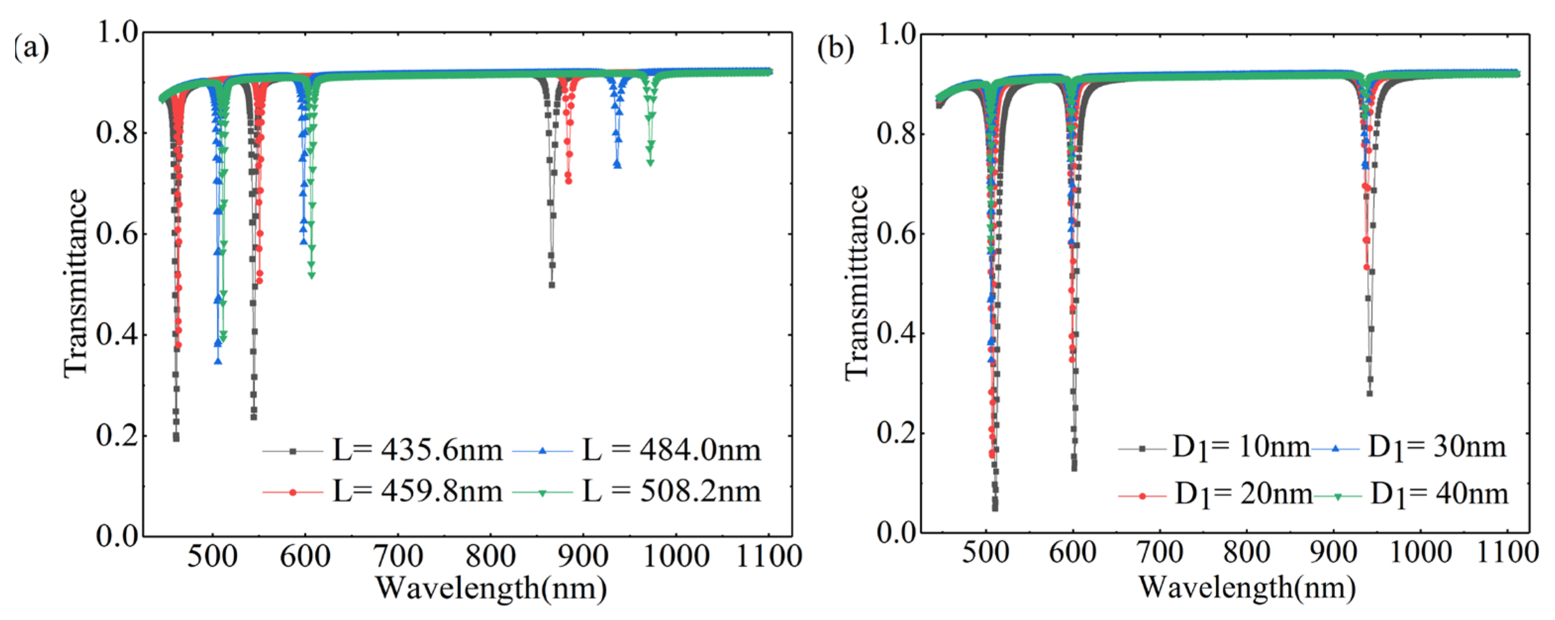
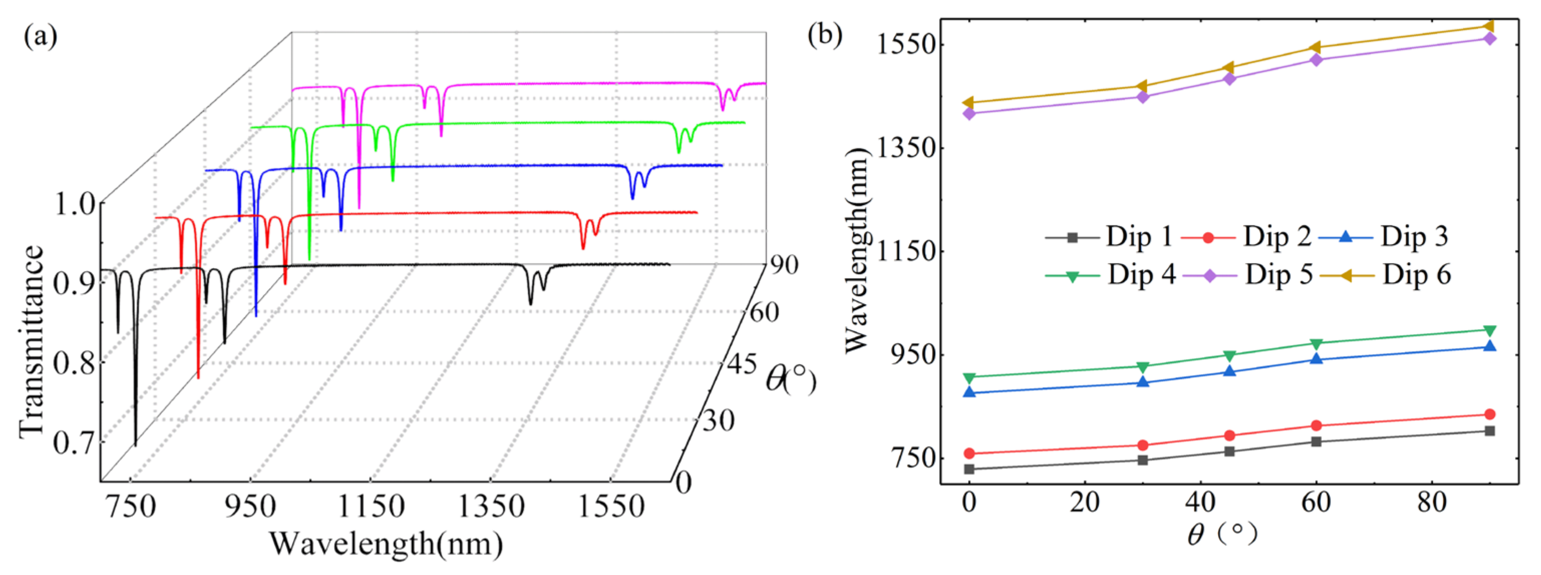
3.3. Realization of Tunable PIT

In Figure 8a, an applied altering current is added to both sides of the two triangles which are filled with NLC E7. As an anisotropic uniaxial crystal, the ordinary refractive index ( n o ) and the extraordinary refractive index ( n e ) of E7 can be fitted into the extended Cauchy equations according to the previous work of Li et al. [39]:
n e , o = A e , o + B e , o λ 2 + C e , o λ 4
Herein, λ is the wavelength of the incident light, and the coefficients at 25 °C are A e = 1.754, B e = 10.08, C e = 0.1709, A o = 1.527, B o = 10.16, and C o = 0.4898. Furthermore, the effective refractive index can be calculated as follows [40]:
n = n e n o n e 2 cos 2 θ + n o 2 sin 2 θ
where θ means the director angle between E7 and the left side of the waveguide. According to Equations (9) and (10), n as a function of λ and θ is shown in Figure 8b. n rises with the decreasing λ and increasing θ .
In Figure 9a, it is shown that there is a redshift at each resonance wavelength, with the transmittance being almost unchanged when θ is increased from 0° to 90°. Figure 9b shows that six dips corresponding to the resonance wavelengths from left to right in Figure 9a have the same tendency with the increase in θ . The characteristics indicate that the transmission spectra can be manipulated by rotating θ to vary the n of E7.
According to [31], the rise time τ r (the time E7 turns to a specific angle with an altering current applied), the decay time τ d (the time E7 turns back to its original state with the electric field removed), and the threshold voltage V t can be expressed as the following equations:
τ d = γ 1 d 2 K 22 π 2
τ r = τ d ( V / V t ) 2 1
V t = π K 22 ε 0 Δ ε
where γ 1 is the rotational viscosity, d is the thickness of the layer, K 22 is the bend elastic constant, and Δ ε is the dielectric anisotropy. The response time of E7 can be obtained from the sum of τ r and τ d . When the applied voltage V exceeds V t , the angle of E7 is linear to V [38]. In general, the response time of the NLC is within a range of milliseconds. However, it is reported that the response time can be up to 100 μ s in nanoscale voids.

3.4. Temperature Analysis of PIT

Given that E7 is sensitive to temperature change, the effects of temperature on the performance of the structure in Figure 8a were studied. In Table 1, the values of the coefficients of the liquid crystal are shown, corresponding to different temperatures [40].
The detection range was set as 25–45 °C. Owing to the extremely small thermal expansion of silver and silicon, the detection range does not cause an apparent deformation of the structure. The variations of the n of E7, which lead to a shift in resonance wavelengths, can be affected by the temperature change. In Figure 10, the shift in each dip from left to right has a linear relationship with the temperature change. Expressed as S T = Δ λ / Δ T , the maximal temperature sensitivity of this structure is 0.29 nm/°C at dip 6. There is a comparison between this work and previous works in Table 2. The structure we propose displays a high refractive index sensitivity and temperature sensitivity compared with other works, which suggests that it can be employed as a multifunctional sensor with good performance.
The structures can be fabricated by focused ion beam (FIB) lithography, using the focused ion beam to write the pattern above onto the silicon substrate. A FIB can be applied to produce three-dimensional hierarchical plasmonic nanostructures because of its high spatial resolution and smaller beam size compared with electron beam lithography. The FIB technique guarantees the reproducibility and tunability of plasmonic nanostructures [41,42,43,44,45,46,47,48,49].
Table 2. Comparison between previous works and this work.
ReferenceStructureS (nm/RIU)ST (nm/°C)
[50]Side-coupled hexagonal cavities9170.45
[51]All-metal metasurface-0.27
[52]Elliptical plasmonic waveguide resonator9500.01
[53]Defect resonator coupled with a waveguide6520.225
[5]Side-coupled rectangular cavity12710.47
[54]Plasmonic waveguide system13300.12
This workTwo triangles coupled with waveguide9330.29

4. Conclusions

In conclusion, a triangle-coupled waveguide structure with a PIT effect is proposed. The transmission characteristics of the structure were studied numerically by FDTD. In addition, NLC E7, whose effective refractive index varied with the external electric field, was added into the triangles to realize the tunability of PIT. The sensitivities of the proposed structure were calculated as 960 nm/RIU and 0.29 nm/°C. Hence, these results offer us possibilities in the realization of photonic devices in highly integrated circuits for the propagation and control of light.

Author Contributions

Conceptualization, J.Z. and H.F.; methodology, J.Z.; software, J.Z.; validation, J.Z., H.F. and Y.G.; formal analysis, J.Z.; investigation, J.Z.; resources, J.Z.; data curation, J.Z.; writing—original draft preparation, J.Z.; writing—review and editing, C.L., D.F., J.W., L.W., Z.Z. and L.R.; visualization, J.Z.; supervision, Y.G.; project administration, Y.G.; funding acquisition, Y.G. All authors have read and agreed to the published version of the manuscript.

Funding

This research was funded by the Natural Science Foundation of Heilongjiang Province (Grant No. LH2019F047), the Project of the Central Government Supporting the Reform and Development of Local Colleges and Universities (Grant No. 2020YQ01), the Heilongjiang University Outstanding Youth Science Fund of Heilongjiang University (JCL201404), the Heilongjiang University Youth Science Fund Project (QL201301), and The Science and Technology Research Project of the Education Department of Heilongjiang Province (12541633).

Institutional Review Board Statement

Not applicable.

Informed Consent Statement

Not applicable.

Data Availability Statement

The available data have already been stated in the article.

Acknowledgments

Structure numerical simulation was provided by Lumerical Solutions, Inc.

Conflicts of Interest

The authors declare no conflict of interest.

References

  1. Barnes, W.L.; Dereux, A.; Ebbesen, T.W. Surface plasmon subwavelength optics. Nature 2003, 424, 824–830. [Google Scholar] [CrossRef] [PubMed]
  2. Gramotnev, D.K.; Bozhevolnyi, S.I. Plasmonics beyond the diffraction limit. Nat. Photonics 2010, 4, 83–91. [Google Scholar] [CrossRef]
  3. Jeong, J.; Goldflam, M.D.; Campione, S.; Briscoe, J.L.; Vabishchevich, P.P.; Nogan, J.; Sinclair, M.B.; Luk, T.S.; Brener, I. High Quality Factor Toroidal Resonances in Dielectric Metasurfaces. ACS Photonics 2020, 7, 1699–1707. [Google Scholar] [CrossRef]
  4. Ai, H.; Kang, Q.; Wang, W.; Guo, K.; Guo, Z. Multi-Beam Steering for 6G Communications Based on Graphene Metasurfaces. Sensors 2021, 21, 4784. [Google Scholar] [CrossRef] [PubMed]
  5. Moradiani, F.; Farmani, A.; Mozaffari, M.H.; Seifouri, M.; Abedi, K. Systematic engineering of a nanostructure plasmonic sensing platform for ultrasensitive biomaterial detection. Opt. Commun. 2020, 474, 126178. [Google Scholar] [CrossRef]
  6. Xie, L.; Gao, W.; Shu, J.; Ying, Y.; Kono, J. Extraordinary sensitivity enhancement by metasurfaces in terahertz detection of antibiotics. Sci. Rep. 2015, 5, 8671. [Google Scholar] [CrossRef] [PubMed]
  7. Lee, D.-K.; Kang, J.-H.; Lee, J.-S.; Kim, H.-S.; Kim, C.; Hun Kim, J.; Lee, T.; Son, J.-H.; Park, Q.H.; Seo, M. Highly sensitive and selective sugar detection by terahertz nano-antennas. Sci. Rep. 2015, 5, 15459. [Google Scholar] [CrossRef]
  8. Naheed, M.; Faryad, M. Excitation of surface plasmon–polariton waves at the interface of a metal and an isotropic chiral material in the prism-coupled configurations. Eur. Phys. J. Plus 2020, 135, 1–15. [Google Scholar] [CrossRef]
  9. Jeon, T.-I.; Grischkowsky, D. THz Zenneck surface wave (THz surface plasmon) propagation on a metal sheet. Appl. Phys. Lett. 2006, 88, 061113. [Google Scholar] [CrossRef] [Green Version]
  10. Saxler, J.; Rivas, J.G.; Janke, C.; Pellemans, H.P.M.; Bolívar, P.H.; Kurz, H. Time-domain measurements of surface plasmon polaritons in the terahertz frequency range. Phys. Rev. B 2004, 69, 155427. [Google Scholar] [CrossRef]
  11. Martl, M.; Darmo, J.; Unterrainer, K.; Gornik, E. Excitation of terahertz surface plasmon polaritons on etched groove gratings. J. Opt. Soc. Am. B 2009, 26, 554–558. [Google Scholar] [CrossRef]
  12. Fang, Y.; Sun, M. Nanoplasmonic waveguides: Towards applications in integrated nanophotonic circuits. Light. Sci. Appl. 2015, 4, e294. [Google Scholar] [CrossRef] [Green Version]
  13. Fleischhauer, M. Electromagnetically induced transparency and coherent-state preparation in optically thick media. Opt. Express 1999, 4, 107–112. [Google Scholar] [CrossRef] [PubMed]
  14. Fleischhauer, A.; Lukin, M.D.; Mair, A.; Phillips, D.F.; Walsworth, R.L. Storage of Light in Atomic Vapor. Phys. Rev. Lett. 2001, 86, 783–786. [Google Scholar]
  15. Zhang, B.; Guo, F.; Wang, J.; Bai, H.; Guo, R.; Zhang, L.; Huang, Y. Plasmonically induced reflection in MIM plasmonic waveguide resonator system. Optik 2018, 171, 161–166. [Google Scholar] [CrossRef]
  16. Zhang, Z.D.; Wang, R.B.; Zhang, Z.Y.; Tang, J.; Zhang, W.D.; Xue, C.Y.; Yan, S.B. Electromagnetically Induced Transparency and Refractive Index Sensing for a Plasmonic Waveguide with a Stub Coupled Ring Resonator. Plasmonics 2017, 12, 1007–1013. [Google Scholar] [CrossRef]
  17. Ruan, B.; You, Q.; Zhu, J.; Wu, L.; Guo, J.; Dai, X.; Xiang, Y. Improving the Performance of an SPR Biosensor Using Long-Range Surface Plasmon of Ga-Doped Zinc Oxide. Sensors 2018, 18, 2098. [Google Scholar] [CrossRef] [Green Version]
  18. Fang, Y.-T.; Hu, J.-X.; Wang, J.-J. Double-Frequency Filter Based on Coupling of Cavity Modes and Surface Plasmon Polaritons. IEEE Photonics J. 2014, 6, 4800307. [Google Scholar] [CrossRef]
  19. Kwon, M.-S. Metal Stripe Waveguide Based Interferometer-Type Sensor Working in an Aqueous Solution With a Low Refractive Index. J. Light. Technol. 2012, 30, 2035–2041. [Google Scholar] [CrossRef]
  20. Ma, F.S.; Lee, C. Optical Nanofilters Based on Meta-Atom Side-Coupled Plasmonics Metal- Insulator-Metal Waveguides. J. Light. Technol. 2013, 31, 2876–2880. [Google Scholar] [CrossRef] [Green Version]
  21. Chen, J.; Li, Y.; Chen, Z.; Peng, J.; Qian, J.; Xu, J.; Sun, Q. Tunable Resonances in the Plasmonic Split-Ring Resonator. IEEE Photonics J. 2014, 6, 1–6. [Google Scholar] [CrossRef]
  22. Bahadori, M.; Eshaghian, A.; Mehrany, K. A Circuit Model for Analysis of Metal-Insulator-Metal Plasmonic Comple-mentary Split-Ring Resonators. J. Light. Technol. 2014, 32, 2659–2665. [Google Scholar] [CrossRef]
  23. Xiao, S.; Wang, T.; Liu, T.; Yan, X.; Li, Z.; Xu, C. Active modulation of electromagnetically induced transparency analogue in terahertz hybrid metal-graphene metamaterials. Carbon 2018, 126, 271–278. [Google Scholar] [CrossRef] [Green Version]
  24. Xia, S.; Zhai, X.; Wang, L.-L.; Sun, B.; Liu, J.-Q.; Wen, S.-C. Dynamically tunable plasmonically induced transparency in sinusoidally curved and planar graphene layers. Opt. Express 2016, 24, 17886–17899. [Google Scholar] [CrossRef] [PubMed]
  25. Rigosi, A.F.; Liu, C.-I.; Wu, B.Y.; Lee, H.-Y.; Kruskopf, M.; Yang, Y.; Hill, H.M.; Hu, J.; Bittle, E.G.; Obrzut, J.; et al. Examining epitaxial graphene surface conductivity and quantum Hall device stability with Parylene passivation. Microelectron. Eng. 2018, 194, 51–55. [Google Scholar] [CrossRef] [PubMed]
  26. Kasani, S.; Curtin, K.; Wu, N.Q. A review of 2D and 3D plasmonic nanostructure array patterns: Fabrication, light man-agement and sensing applications. Nanophotonics 2019, 8, 2065–2089. [Google Scholar] [CrossRef]
  27. Kao, Y.-Y.; Chao, P.C.-P. A New Dual-Frequency Liquid Crystal Lens with Ring-and-Pie Electrodes and a Driving Scheme to Prevent Disclination Lines and Improve Recovery Time. Sensors 2011, 11, 5402–5415. [Google Scholar] [CrossRef]
  28. Chao, C.-T.C.; Chau, Y.-F.C.; Huang, H.J.; Kumara, N.T.R.N.; Kooh, M.R.R.; Lim, C.M.; Chiang, H.-P. Highly Sensitive and Tunable Plasmonic Sensor Based on a Nanoring Resonator with Silver Nanorods. Nanomaterials 2020, 10, 1399. [Google Scholar] [CrossRef]
  29. Kekatpure, R.D.; Hryciw, A.C.; Barnard, E.S.; Brongersma, M.L. Solving dielectric and plasmonic waveguide dispersion relations on a pocket calculator. Opt. Express 2009, 17, 24112–24129. [Google Scholar] [CrossRef] [Green Version]
  30. Johnson, P.B.; Christy, R.W. Optical Constants of the Noble Metals. Phys. Rev. B 1972, 6, 4370–4379. [Google Scholar] [CrossRef]
  31. Wang, S.; Zhao, T.; Yu, S.; Ma, W. High-Performance Nano-Sensing and Slow-Light Applications Based on Tunable Multiple Fano Resonances and EIT-Like Effects in Coupled Plasmonic Resonator System. IEEE Access 2020, 8, 40599–40611. [Google Scholar] [CrossRef]
  32. Hu, F.; Yi, H.; Zhou, Z. Band-pass plasmonic slot filter with band selection and spectrally splitting capabilities. Opt. Express 2011, 19, 4848–4855. [Google Scholar] [CrossRef]
  33. Chen, J.; Badioli, M.; Alonso-González, P.; Thongrattanasiri, S.; Huth, F.; Osmond, J.; Spasenović, M.; Centeno, A.; Pesquera, A.; Godignon, P.; et al. Optical nano-imaging of gate-tunable graphene plasmons. Nature 2012, 487, 77–81. [Google Scholar] [CrossRef] [PubMed] [Green Version]
  34. Xia, S.; Zhai, X.; Huang, Y.; Liu, J.-Q.; Wang, L.-L.; Wen, S.-C. Multi-band perfect plasmonic absorptions using rectangular graphene gratings. Opt. Lett. 2017, 42, 3052–3055. [Google Scholar] [CrossRef] [PubMed]
  35. Shi, H.; Yan, S.; Yang, X.; Su, H.; Wu, X.; Hua, E. Nanosensor Based on Fano resonance in a metal-insulator-metal waveguide structure coupled with a half-ring. Results Phys. 2021, 21, 103842. [Google Scholar] [CrossRef]
  36. Shen, X.; Zhao, L.; Xia, D. Research on the Disc Sensitive Structure of a Micro Optoelectromechanical System (MOEMS) Resonator Gyroscope. Micromachines 2019, 10, 264. [Google Scholar] [CrossRef] [PubMed] [Green Version]
  37. Pallapa, M.; Yeow, J.T.W. Design, Fabrication and Testing of a Polymer Composite Based Hard-Magnetic Mirror for Bi-omedical Scanning Applications. J. Electrochem. Soc. 2013, 161, B3006–B3013. [Google Scholar] [CrossRef]
  38. Yong, Y.K.; Moheimani, S.O.R.; Kenton, B.J.; Leang, K.K. Invited Review Article: High-speed flexure-guided nanopositioning: Mechanical design and control issues. Rev. Sci. Instrum. 2012, 83, 121101. [Google Scholar] [CrossRef] [PubMed]
  39. Shao, H.; Guan, B.; Cui, L.; Cui, N.; Zhang, Y.; Zeng, Y. Transverse-mode control in VCSELs by electrically tunable liquid crystal mode filters. AIP Adv. 2021, 11, 015225. [Google Scholar] [CrossRef]
  40. Chiang, L.-Y.; Wang, C.-T.; Lin, T.-S.; Pappert, S.; Yu, P. Highly sensitive silicon photonic temperature sensor based on liquid crystal filled slot waveguide directional coupler. Opt. Express 2020, 28, 29345–29356. [Google Scholar] [CrossRef]
  41. Li, J.; Wen, C.-H.; Gauza, S.; Lu, R.; Wu, S.-T. Refractive Indices of Liquid Crystals for Display Applications. J. Disp. Technol. 2005, 1, 51–61. [Google Scholar] [CrossRef]
  42. Khan, K.R.; Mnaymneh, K.; Awad, H.; Hasan, I. Slow light propagation in tunable nanoscale photonic crystal cavity filled with nematic liquid crystal. Opt. Eng. 2014, 53, 102705. [Google Scholar] [CrossRef]
  43. Nie, X.; Xianyu, H.; Lu, R.; Wu, T.X.; Wu, S.-T. Pretilt Angle Effects on Liquid Crystal Response Time. J. Disp. Technol. 2007, 3, 280–283. [Google Scholar] [CrossRef]
  44. Hu, J.; Zhang, H.; Li, Z.; Zhao, C.; Xu, Z.; Pan, Q. Object traversing by monocular UAV in outdoor environment. Asian J. Control 2020, 23, 2766–2775. [Google Scholar] [CrossRef]
  45. Qiao, G.; Ding, L.; Zhang, L.; Yan, H. Accessible tourism: A bibliometric review (2008–2020). Tour. Rev. 2021. (ahead-of-print). [Google Scholar] [CrossRef]
  46. Wang, M.; Jiang, C.; Zhang, S.; Song, X.; Tang, Y.; Cheng, H.-M. Reversible calcium alloying enables a practical room-temperature rechargeable calcium-ion battery with a high discharge voltage. Nat. Chem. 2018, 10, 667–672. [Google Scholar] [CrossRef] [PubMed]
  47. Yan, Y.; Feng, L.; Shi, M.; Cui, C.; Liu, Y. Effect of plasma-activated water on the structure and in vitro digestibility of waxy and normal maize starches during heat-moisture treatment. Food Chem. 2020, 306, 125589. [Google Scholar] [CrossRef]
  48. Zhang, X.; Tang, Y.; Zhang, F.; Lee, C.-S. A Novel Aluminum-Graphite Dual-Ion Battery. Adv. Energy Mater. 2016, 6, 1502588. [Google Scholar] [CrossRef] [Green Version]
  49. Mu, S.; Liu, Q.; Kidkhunthod, P.; Zhou, X.; Wang, W.; Tang, Y. Molecular grafting towards high-fraction active nanodots implanted in N-doped carbon for sodium dual-ion batteries. Natl. Sci. Rev. 2020, 8, 7. [Google Scholar] [CrossRef]
  50. Xie, Y.; Huang, Y.; Xu, W.; Zhao, W.; He, C. A Plasmonic Temperature-Sensing Structure Based on Dual Laterally Side-Coupled Hexagonal Cavities. Sensors 2016, 16, 706. [Google Scholar] [CrossRef] [Green Version]
  51. Chen, J.; Zhang, H.; Liu, G.; Liu, J.; Liu, Y.; Tang, L.; Liu, Z. High-quality Temperature Sensor Based on the Plasmonic Resonant Absorber. Plasmonics 2018, 14, 279–283. [Google Scholar] [CrossRef]
  52. Dehghan, B.; Sadeghi, M.; Adelpour, Z. Refractive Index, Temperature and Pressure of Elliptical Plasmonic Waveguide Resonator. Rev. Geintec-Gestao Inov. E Tecnol. 2021, 11, 2029–2037. [Google Scholar] [CrossRef]
  53. Chen, F.; Li, J. Refractive index and temperature sensing based on defect resonator coupled with a MIM waveguide. Mod. Phys. Lett. B 2019, 33, 126178. [Google Scholar] [CrossRef]
  54. Kong, Y.; Qiu, P.; Wei, Q.; Quan, W.; Wang, S.; Qian, W. Refractive index and temperature nanosensor with plasmonic waveguide system. Opt. Commun. 2016, 371, 132–137. [Google Scholar] [CrossRef]
Figure 1. (a) Three-dimensional configuration of the triangle-coupled MDM waveguide structure; (b) transmission spectra of the structure calculated by CMT and FDTD.
Photonics 09 00100 g001
Figure 2. Transmission spectra of the structure with variables: (a) L; (b) D1.
Photonics 09 00100 g002
Figure 3. (a) Two-dimensional configuration of the side-coupled MDM waveguide structure with two triangles; (b) transmission spectra of the structure with and without the upper triangle.
Photonics 09 00100 g003
Figure 4. Magnetic field distributions corresponding to positions at: (a) H1; (b) I1; (c) J1; (d) K1; (e) H2; (f) I2; (g) J2; (h) K2; (i) H3; (j) I3; (k) J3; (l) K3, in Figure 3b.
Photonics 09 00100 g004
Figure 5. Current densities corresponding to positions at: (a) H1; (b) J1; (c) H2; (d) J2; (e) H3; (f) J3, in Figure 3b.
Photonics 09 00100 g005
Figure 6. Transmission spectra of PIT with variables: (a) D1; (b) D2.
Photonics 09 00100 g006
Figure 7. (a) Transmission spectra of the structure when changing the refractive index (n) of the material in two triangles; (b) the shifts in resonance wavelengths with different n values.
Photonics 09 00100 g007
Figure 8. (a) Two-dimensional configuration of the structure with NLC E7 added into the triangles; (b) the dependence of the n of E7 on its director angle ( θ ) and the wavelength of incident light.
Photonics 09 00100 g008
Figure 9. (a) Transmission spectra with different θ values of E7; (b) dependence of the resonance wavelength on θ .
Photonics 09 00100 g009
Figure 10. (a) Transmission spectra with different T values of E7; (b) dependence of resonance wavelength on T.
Photonics 09 00100 g010
Table 1. Coefficients of the liquid crystal at different temperatures.
T (°C)AeBeCeAoBoCo
251.75410.080.17091.52710.160.4898
301.74610.930.48541.52710.620.1626
351.73710.630.03571.52810.670.2551
401.72610.570.17121.53010.050.2575
451.71310.660.31711.53210.130.2511
Publisher’s Note: MDPI stays neutral with regard to jurisdictional claims in published maps and institutional affiliations.

