Article

Implementation of Logic Gates in an Erbium-Doped Fiber Laser (EDFL): Numerical and Experimental Analysis

by
Samuel Mardoqueo Afanador Delgado
1,
José Luis Echenausía Monroy
1,2,
Guillermo Huerta Cuellar
1,
Juan Hugo García López
1 and
Rider Jaimes Reátegui
1,*
1
Dynamical Systems Laboratory, CULagos, Universidad de Guadalajara, Centro Universitario de los Lagos, Enrique Díaz de León 1144, Paseos de la Montaña, Lagos de Moreno 47460, Mexico
2
Applied Physics Division, Center for Scientific Research and Higher Education at Ensenada (CICESE), Carr. Ensenada-Tijuana 3918, Zona Playitas, Ensenada 22860, Mexico
*
Author to whom correspondence should be addressed.
Photonics 2022, 9(12), 977; https://doi.org/10.3390/photonics9120977
Submission received: 16 November 2022 / Revised: 5 December 2022 / Accepted: 6 December 2022 / Published: 12 December 2022
(This article belongs to the Special Issue Lasers and Dynamic of Systems)

Abstract

:
At a time when miniaturization and optimization of resources are in the foreground, the development of devices that can perform various functions is a primary goal of technological development. In this work, the use of an Erbium-Doped Fiber Laser (EDFL) is proposed as a basic system for the generation of an optical logic gate. Taking advantage of the dynamic richness of this type of laser and its use in telecommunication systems, the dynamic response is analyzed when the system is perturbed by a digital signal. The emission response of the system is controlled by the intensity of the digital signal, so that it is possible to obtain different logic operations. The numerical results are in good agreement with the experimental observations. The presented work raises new aspects in the use of chaotic systems as a means of obtaining optical logic gates.

1. Introduction

In optical fibers doped with rare earths (also called laser fibers), absorption processes take place, both spontaneous and stimulated emission, when excited with certain energies [1,2,3,4,5]. These characteristics give this type of fibers the necessary properties for their use as optical amplifiers, lasers, sensors, to name a few. The ability of the fibers to generate light in different wavelengths by doping with rare earths has been used in fields such as telecommunications, signal processing, medicine, study of meteorological phenomena and modeling of real multistable systems, all this with the help of various pumping methods and laser resonators.
The research and commercialization of Erbium-Doped Fiber Lasers has recently intensified. Reasons include their long pumping interaction with active ions, high gain margin, transverse mode of operation, tiny size equivalent to the width of a hair, high threshold for damage, excellent heat dissipation, and the fact that they have no bandwidth limitation, leading to better efficiency in laser pumping applications [6,7,8]. Although their properties are diverse and rich, this type of laser is also relevant from the perspective of nonlinear systems, as they are very sensitive to external disturbances that lead to destabilization of the laser dynamics, causing them to oscillate in a nonlinear regime, leading to chaotic behavior [9,10].
Taking advantage of the dynamic properties of chaotic systems, the so-called “chaos computing” has become popular. It is essentially based on the use of an analog chaotic oscillator that emulates the behavior of various logic gates, allowing it to switch between different modes of operation and thus the resolution of various arithmetic operations [11]. In this sense, many proposals on chaotic logic gates have been made, such as in [12], where a SR (Set-Reset) flip-flop has been developed based on NOR gates implemented by a Chua circuit. In [13] it is described how to implement fundamental logic gates based on a logistic map. In [14] the fundamental NOR gate is implemented based on threshold control of chaotic systems. The use of a nonlinear system with noise is discussed in [15], where logic functions are obtained by changing the nonlinearity of the model, and in [16] a circuit with dynamic logic architecture is presented, showing NOR, NAND and XOR logic gates. Potential applications of chaos computing can be approached by changing the pump inputs in time in a CO 2 laser with modulated losses, where changing the modulation depth of the periodic losses leads to different chaotic and periodic attractors [17,18].
Most of the logic gates described above are based on the use of chaotic systems with two attractors located at different equilibrium points. This allows for a dynamic discretization that takes into account the response of the system to a bias and the change in behavior due to the position of the attractor [19,20,21]. Considering the possible application of a chaotic system that can function as a logic gate based on a telecommunication system, and the few works that deal with this topic from the optical systems point of view [22,23], the present work deals with the generation of AND and NOR logic gates using an Erbium-Doped Fiber Laser as a dynamic system. By perturbing the system with a bias signal, it is possible to change the operating regime of the laser, obtaining a completely different logic state that is stable in time. The numerically obtained results are experimentally validated and largely agree.
The remainder of the paper deals with the following topics: Section 2 describes the EDFL mathematical system. The implemented experimental setup and the natural dynamics of the system are also described in this section. The obtained results are described in detail in Section 3. The discussion of the obtained results is given in Section 4. Section 5 describes the conclusions, implications, and future work.

2. Materials and Methods

2.1. Numerical Model

The dynamics of an EDFL pump diode are described by Equation (Section 2.1), and better described in [24,25,26,27].
d P d t = 2 L T r P { r w α 0 [ N ( ξ 1 ξ 2 ) 1 ] α t h } + P s p , d N d t = σ 12 r w P π r 0 2 ( N ξ 1 1 ) N τ + P p u m p ,
where P is the power of the laser in the cavity, N = ( 1 / n 0 L ) 0 L N 2 ( z ) d z is the average of the upper level of the laser potential, where N 2 is the upper plane in the z-coordinate, (propagation direction of the laser emission), n 0 is the refractive index of the cold core of the erbium-doped fiber, ξ 1 and ξ 2 define the relationship between the cross sections and the ground absorption state. The variable T r is the complete travel time of a photon in the cavity, α 0 is the absorption coefficient of the erbium-doped fiber, α t h is the threshold loss counter of the laser cavity, where τ is the lifetime of an excited erbium ion, and r w is the factor comprising the coincidence between the fundamental mode of the laser and the volume of the erbium-doped core.
The spontaneous emission within the fundamental mode of the laser is defined as:
P s p = N 10 3 T r τ λ g ω 0 2 r 0 2 α 0 L 4 π 2 σ 12 ,
where λ g is the wavelength of the laser, 1.5   μ m . The pump power is equivalent to:
P p u m p = P p 1 exp [ α 0 β L ( 1 N ) ] N 0 π r 0 2 L , P p = p [ 1 m sin ( 2 π f m t ) ] .
In Equation (3), P p is the pump power at the fiber input and β is a dimensionless coefficient. When the input current of the laser diode is modulated with a harmonic signal, the EDFL describes the behavior given in Equation (1), which represents the coexistence of up to four attractors defined as periods one, three, four, and five (P 1 , P 3 , P 4 , and P 5 ), as shown by the red dashed line in Figure 1a.
To understand the dynamics of the EDFL, the bifurcation diagram of the local maxima of the laser intensity as a function of the pump modulation frequency f m is calculated. To perform numerical simulation, the equations described in Equation (1) are normalized to obtain Equation (4). The normalization procedure and further details can be found in the appendix of reference [5,28], and the system coefficients are described in Table 1.
x ˙ = a x y b x + c ( y + r w ) , y ˙ = d x y ( y + r w ) + e 1 exp β α 0 L ( 1 y + r w ξ 2 r w ) .
At a modulation amplitude m = 1 , the laser system exhibits dynamic richness by varying the modulation frequency, showing a bifurcation diagram as in Figure 1a. The sequence of periodic orbits (P3, P4, P5, etc.) in the periodically modulated EDFL in Figure 1 is known as Period-Adding Cascades (PAC) and typically arises as a saddle-node bifurcation in which there is a homoclinic to a periodic orbit. In the context of infrared lasers, PAC has also been observed in simulations, and by numerical continuation in bifurcation analysis in the CO 2 laser with a saturable absorber in [29,30].

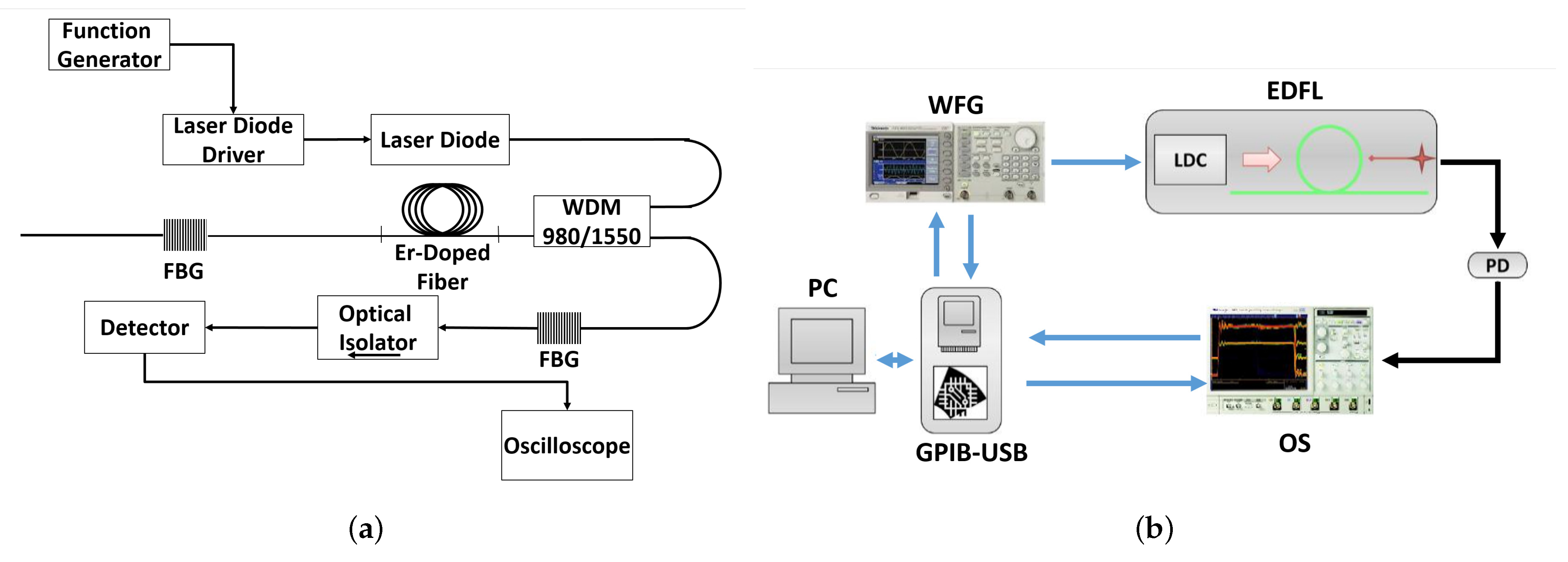
2.2. Experimental Set-Up

The experimental setup used in this work, shown in Figure 2, consists of a 1560 nm EDFL pumped by a 977 nm Laser Diode (LD). The laser cavity consists of an erbium-doped fiber of approximately 88 cm long with a core diameter of 2.7 µm and two fiber Bragg gratings (FBG1 and FBG2) with reflectivities of 100 % and 95.88 % , respectively. All components are interconnected with a monomode fiber. The laser diode is controlled by the pump controller (LDC). For all experiments performed, the pump current is set to 145.5 mA (20 nW). The choice of the pump current is to ensure a relaxation frequency of the laser close to F r = 30 kHz. To control the dynamics of the laser and to achieve the different logic gates, both the harmonic modulation and the bias signal are injected into the pump diode via a function generator (WFG) and a digital interface, respectively.
Figure 1b shows the bifurcation diagram of the experimental system, which agrees with the numerical estimate.

2.3. Methods

For the implementation of the logic gate, a modulation frequency range 40 f m 60 kHz was defined, and the modulation amplitude remains fixed A m = 1 . The frequency selection results in the laser response being at P 2 , as shown in Figure 3. In this case, the bias signal is added to the modulation signal and causes a shift in the laser response that allows switching between different periodic regimes of the system.
Remark 1.
In this work, the dynamic response of the laser is referred to as “period N (P N )”, i.e., N R + . The EDFL system is modulated with a periodic sinusoidal signal that determines the laser emission. A P 1 type output response indicates that the laser emission occurs sequentially with respect to the modulation period. A type P 3 output response, in turn, indicates that three periods of the periodic signal were injected for each pulse of the laser response. Figure 2 illustrates the relationship with the superposition of the laser modulation (black line), the laser response in P 2 (red line) and the type P 1 emission (blue line).
To characterize the response of the EDFL to logic gate generation, we need to define a reference signal I d that represents the bias voltage that is injected into the pumping process, as shown in Equation (5). Consider an input signal I d defined as the sum of two digital decorrelated signals I d = I 1 + I 2 . Since I i are digital signals, i.e., can only take the values 0 and 1, the combination of these signals can only result in four possible logical inputs ( I 1 , I 2 ) : ( 0 , 0 ) , ( 0 , 1 ) , ( 1 , 0 ) , ( 1 , 1 ) .
P p = A m sin ( 2 π f m t ) + A d I d .
Remark 2.
Note that the logical input combinations ( 0 , 1 ) and ( 1 , 0 ) result in the same signal I d , so combining the logical signals ( I 1 , I 2 ) yields only three possible combinations. Thus, the sum of two decorrelated logic signals results in an aperiodic signal with three states, as shown in Figure 4.. For a set of inputs ( 0 , 0 ) , there is a value of I d = 0 . For a combination ( 0 , 1 ) / ( 1 , 0 ) the value of I d = 1 , and finally for ( 1 , 1 ) we have I d = 2 . In our implementation, we propose a digital gain ( A d ) to control the amplification of the generated signal.
Remark 3.
The approach considered in this paper is based on the shift between P 2 and P 1 . P 2 is considered as a logical 1, while the shift to P 1 is a logical 0.

3. Results

The following section describes the results obtained, both for the numerical simulation and for the experimental implementation.

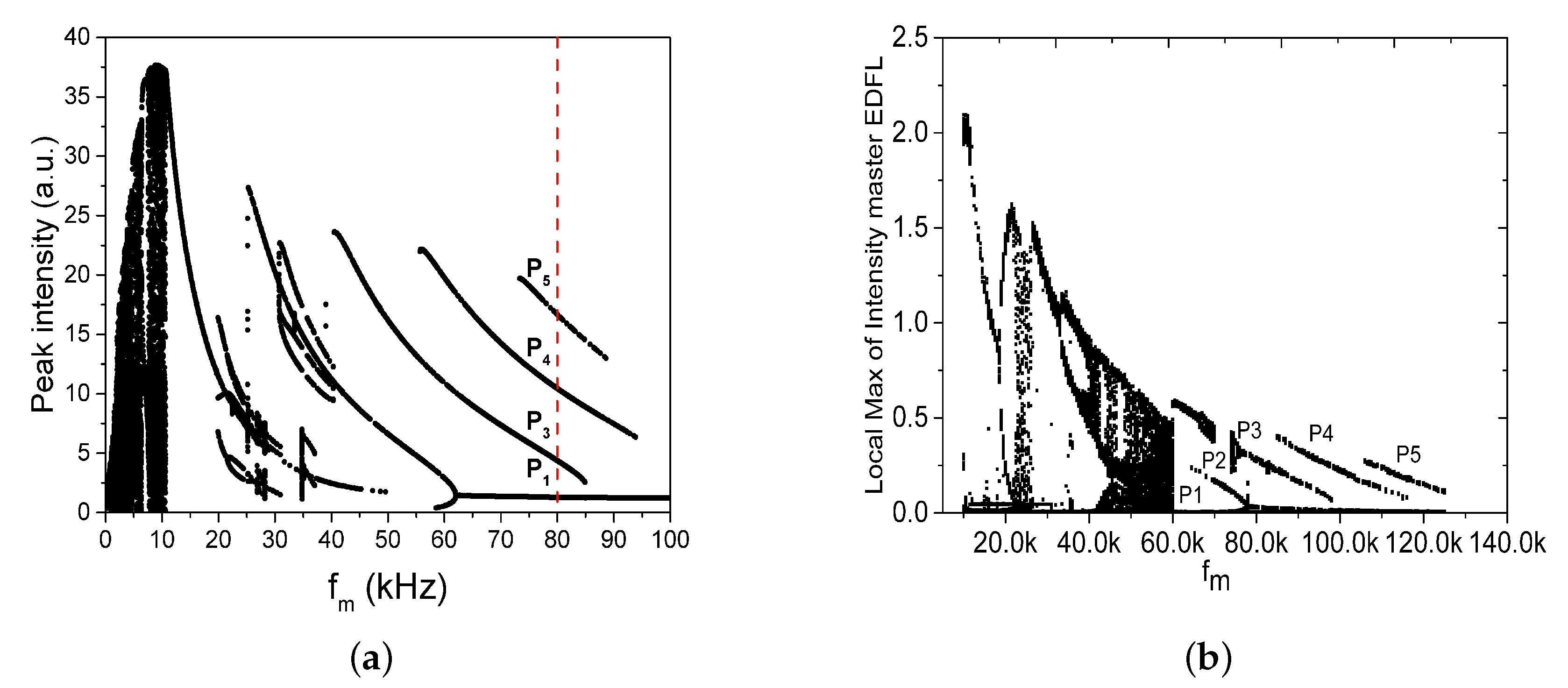
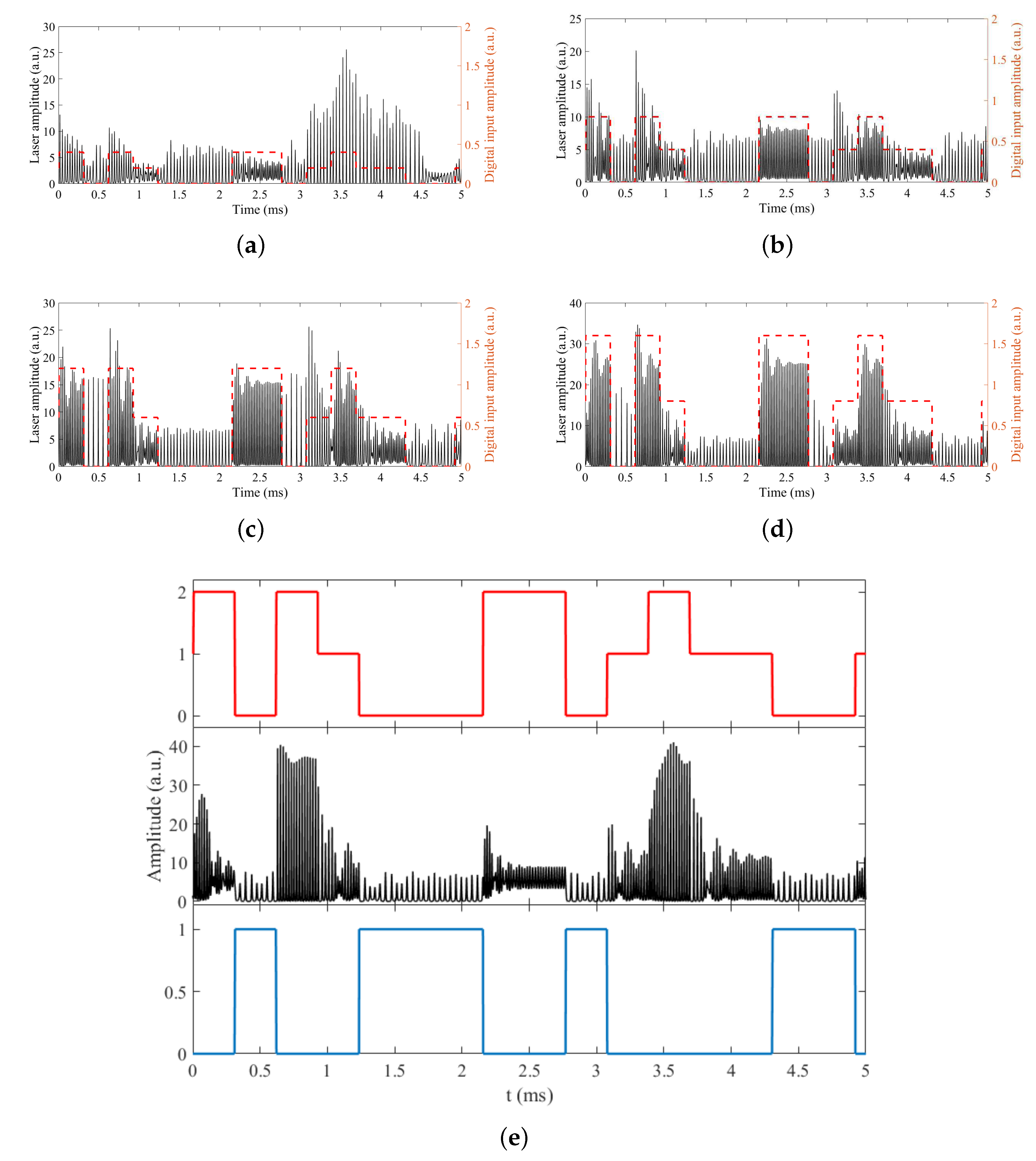
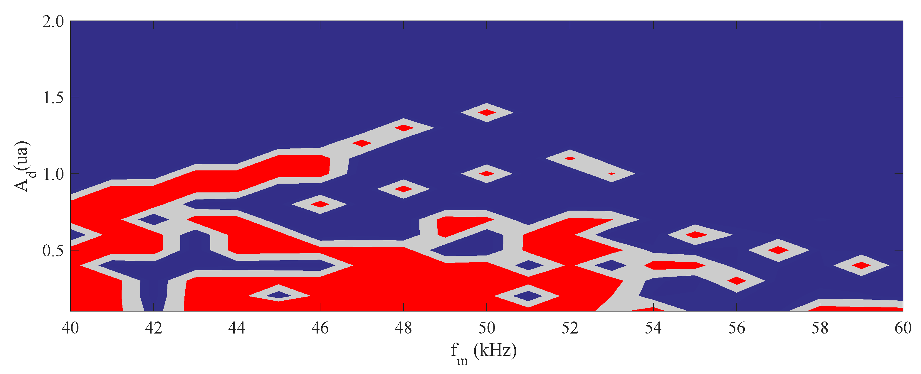
3.1. Numerical Results

Any dynamic system changes its behavior when it is perturbed with the necessary energy. In this case, we assume that the laser changes its behavior when a bias signal is added to the modulation. In our implementation, a square wave signal ( I d ) was added to the laser modulation.
Figure 5a–e shows the effects of the bias signal on the dynamic response of the laser when a fixed modulation frequency is used and the gain of the digital signal is varied. If we use the signal shown in Figure 5e as example, in Figure 5f again shows the digital input signal I d , in which we can observe the three states given by the arithmetic sum of the two decorrelated digital inputs. In Figure 5e we see the behavior of the laser changing its behavior into different periods due to the bias voltage, and in Figure 5g we can see the output of the logic gate, where the states are defined by the change of the period, as mentioned above. Thus, P 2 is assigned a high value and a P 1 is assigned a low value.
Having confirmed the original hypothesis that the system changes its dynamics by injecting a digital signal into the laser pump, a characterization of the laser dynamics was performed using a frequency sweep in the range defined by 40 f m 60 kHz, which was varied in steps of 1 kHz, and the amplitude of the digital signal 0.2 A d 1 was changed in steps of Δ A d = 0.1 (a.u.). For each set of parameters A d , f m , a time series analysis was performed to discretize the laser dynamics taking into account the period changes, resulting in the behavior shown in Figure 6.
On the color map shown in Figure 6, it is possible to distinguish different color regions corresponding to the emission regime of the laser. The gray region has no defined period, the red region corresponds to P 2 , and the blue region corresponds to P 1 . Thus, if we are at a frequency of f m = 44 kHz and the amplitude of the signal is A d = 0.2 (a.u.), the laser will respond with P 2 , while at A d = 0.8 (a.u.) it will respond with P 1 . In this way we can build the logic gates.

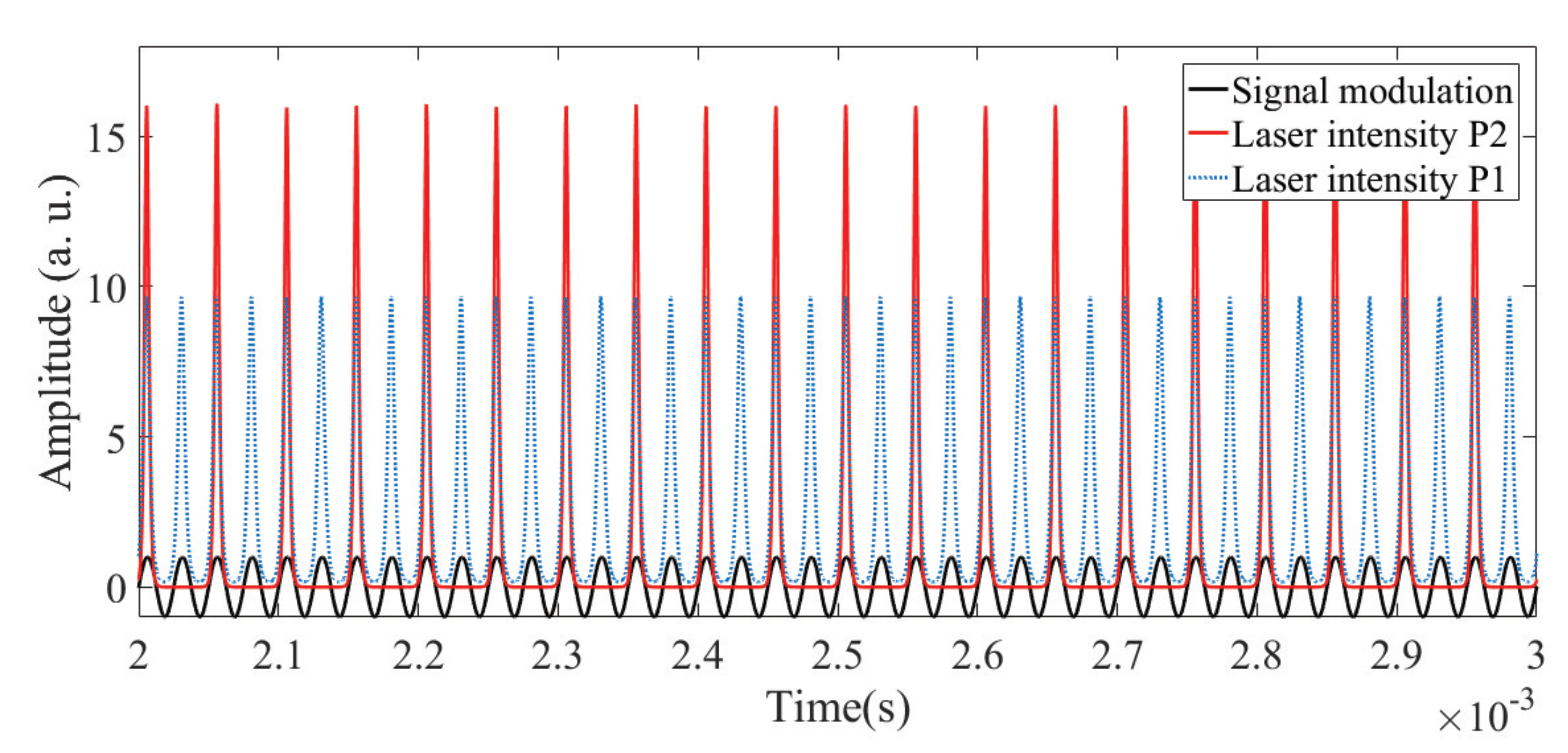
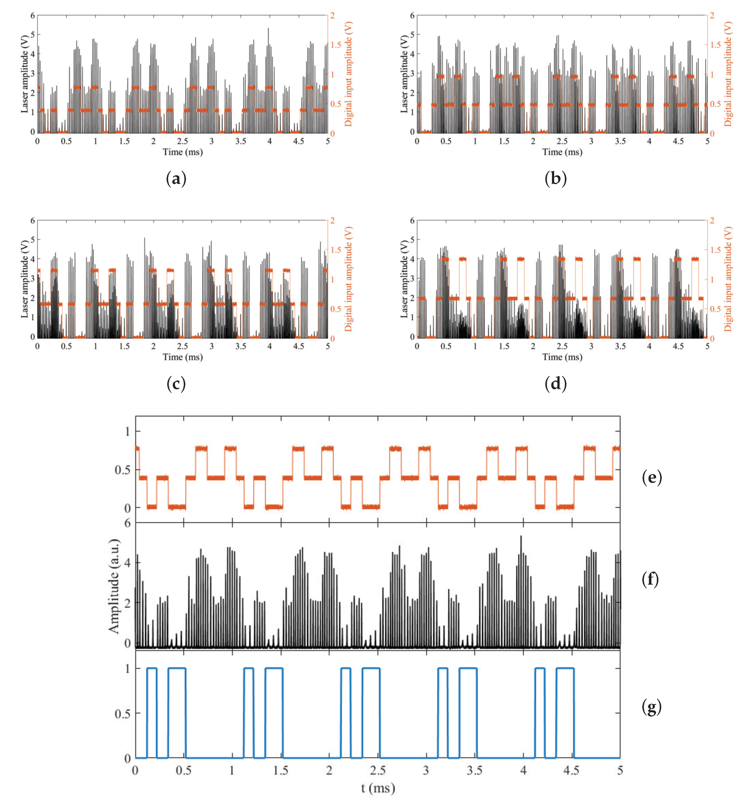
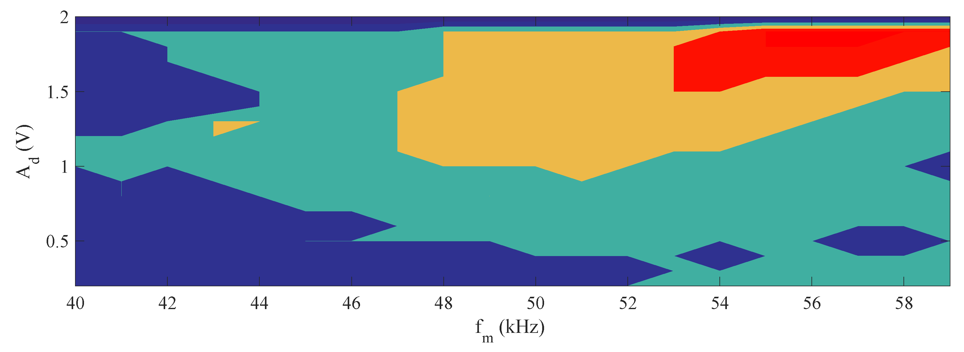
3.2. Experimental Results

To experimentally verify the results of the numerical EDFL model, the following parameters are used: the modulation amplitude remains fixed A m = 1 V, the modulation frequency was varied from 40 f m 60 kHz, the amplitude of the bias 0.2 A d 1 V. The digital inputs I d = I 1 + I 2 were generated using a data acquisition board (DAQ), which was later added to the modulation.
Figure 7 shows the change in laser intensity when the digital signal I d is added to the modulation. The modulation frequency is fixed f m = 40 kHz and the amplitude of the digital signal 0.4 A d 0.8 V. Here (Figure 7a–e), the solid black line represents the laser intensity response and the red line represents the bias signal used. As in the previous section, a change in amplitude A d results in a change in the emission response of the laser. For an amplitude A d > 0.6 V (Figure 7c,d) three periods are shown, one for each level of the signal I d , but for an amplitude A d = 0.4 V the signal oscillates between P 1 and P 2 (Figure 7a).
In Figure 7f,g, the amplitude A d = 0.4 V and the modulation frequency f m = 40 kHz remain fixed. This choice is due to the fact that the laser shows a response between P1 and P2. Figure 7f shows the bias signal I d , Figure 7e shows the laser intensity, and Figure 7g shows the discretized gate output of the laser response. At a value of I d = 0.0 V, the (0,0) state, the laser response is P 2 , while at A d = 0.4 V and A d = 0.8 V, the (0,1)/(1,0) and (1,1) states, respectively, the laser response corresponds to P 1 . If, as mentioned in the methodology section, you define P 2 as logic 1 and the period change to P 1 as logic 0, you obtain a logic gate with the behavior NOR.
Similar to the numerically obtained color map (Figure 6), a corresponding sweep in the modulation frequency and amplitude of the digital signal was performed for the experimental scheme. Once the laser signals are acquired, a time series analysis is performed to determine the period exhibited by the laser for each combination of parameters ( A d , f m ) . The result is the color map shown in Figure 8. In contrast to the numerical model, in which only P 1 and P 2 are represented. In the experimental implementation, we can see four regions corresponding to P 4 (red), P 3 (yellow), P 2 (light blue), and P 1 (dark blue). If we define the modulation frequency f m = 44 kHz and the amplitude of the digital signal A d = 0.4 V, we have P1 for one state (0,0) and P 2 for the other states.

4. Discussion

Since the EDFL is modulated by the current, the system has a defined response when a fixed modulation frequency ( f m ) is added and is insensitive to initial conditions. However, by adding a signal to this modulation, it is possible to vary the current in the system, resulting in a change in the dynamic response of the laser. This phenomenon can be observed both numerically and experimentally in Figure 5 and Figure 7, respectively.
In Figure 5 and Figure 7, it is possible to see that the laser changes its emission period when the amplitude of the bias voltage is increased. This is because the modulation signal oscillates between a positive and a negative voltage, Equations (3) and (5), where the voltage limits are given by A m and the frequency between the positive and/or negative states is given by the ratio f m / 2 and has the same duration. When a constant signal of amplitude A d is added to the laser modulation, the amplitude of the valley A v = A v A d decreases and the amplitude of the peak A p = A p + A d increases. As a result, the time when the modulation signal has a negative value decreases and the positive value increases. This phenomenon is shown in Figure 9.
Considering the type of laser used in the study, the laser shows no emission when the modulation signal has no positive component, while the laser is able to emit when the modulation signal is positive. In this way, the addition of the bias signal increases the probability of laser emission, resulting in a dynamic change from P 2 to P 1 , which is reflected in an increase in the amplitude of laser emission, as shown in Figure 5 and Figure 7.
The color maps in which the dynamics of the laser are discretized (Figure 6 and Figure 8 in numerical and experimental ways, respectively) provide a broader perspective on what happens to the laser when both the modulation frequency and the amplitude of the digital signal are changed. With this discretization, it is possible to create the logic gates by defining a high logic output state when the laser is emitting at P 2 and a logic zero when the laser emission is on P 1 .
Analyzing the results of the numerical implementation (Figure 6) with a frequency of f m = 44 kHz and A d = 0.2 (a.u.), we obtain a NAND logic gate as shown in Table 2. If the parameters are changed, it is possible to obtain a range of gates, i.e., for a bias signal amplitude A d = 0.4 (a.u.) and f m = 42 kHz, the obtained gate will be an XOR. Table 3 shows other gates resulting from changes in the parameter space ( f m , A d )
Similarly, it is possible to determine different logic gates from the dynamic characterization of the experimental system, see Figure 8. Consider A d = 0.5 V and f m = 44 kHz, with this combination of values it is possible to build an XNOR gate using the EDFL. On the other hand, if A d = 0.2 V and a modulation frequency of 42 kHz is used, a NAND gate is obtained. The different logic gates and their corresponding experimental values are described in Table 4.
It is worth noting that the ranges of values and the behavior between the numerically and experimentally determined values are not identical. This is because the numerical model did not take into account or model the noise of the instruments used to generate the signal, the resolution and the noise of the electronic components used to connect the instruments to the laser. However, it is confirmed that it is possible to build logic gates using this method and to change the nature of the gate by changing the parameter space ( f m , A d ) .

5. Conclusions

In the present work, it was possible to develop an optical device capable of solving logical operations and enabling the implementation of logic gates based on the dynamic richness of an EDFL. The operation of the EDFL as a logic gate generator is based on the dynamic richness of the system by injecting a periodic signal into the laser pump.
The obtained results are based on the perturbation of the modulation of an Erbium-Doped Fiber Laser. The system exhibits a dynamical richness ranging from the presence of periodic states to chaos and coexistent states; all of which are caused by the modulation of the system. Starting from this dynamic richness, the behavior of the laser emission is studied when a digital signal with random frequency is added to the laser modulation.
As a result, the EDFL is able to respond constantly to the perturbations induced by the digital signal, which allows the dynamic response to be discretized so that a logic gate generator system can be obtained by optical means.
The numerically obtained results are validated by the characterization of the experimental system. In a space defined by the modulation frequency and the amplitude of the digital signal ( f m , A d ), the system is able to give a consistent response with up to four different logic gates.

Author Contributions

S.M.A.D.: Writing—Original Draft, Writing—Review & Editing, Methodology, Software, Validation, Data Curation, Visualization. J.L.E.M.: Writing—Original Draft, Writing—Review & Editing, Visualization. G.H.C.: Formal analysis, Review & Editing. J.H.G.L.: Writing—Review & Editing, Resources, Project administration. R.J.R.: Supervision, Funding acquisition, Writing—Review & Editing, Conceptualization, Resources, Project administration. All authors have read and agreed to the published version of the manuscript.

Funding

This project was supported by CONACYT under project number 320597.

Institutional Review Board Statement

Not applicable.

Informed Consent Statement

Not applicable.

Data Availability Statement

The data is available on article submitted to Data journal, from MDPI, (ID:2075448) under the title: Numerical and Experimental Data of the Implementation of Logic Gates in an Erbium-Doped Fiber Laser (EDFL), and available at the repository with DOI: 10.17632/ctnhmgbrzz.2.

Acknowledgments

J.L.E.M. thanks CONACYT for financial support (CVU-706850, project: A1-S-26123, and project: 320597). R.J.R. thanks CONACYT for financial support, project No. 320597.

Conflicts of Interest

The authors certify that they have NO affiliations with or involvement in any organization or entity with any financial interest (such as honoraria; educational grants; participation in speakers’ bureaus; membership, employment, consultancies, stock ownership, or other equity interest; and expert testimony or patent-licensing arrangements), or non-financial interest (such as personal or professional relationships, affiliations, knowledge or beliefs) in the subject matter or materials discussed in this manuscript.

References

  1. Digonnet, M.J.; Gaeta, C. Theoretical analysis of optical fiber laser amplifiers and oscillators. Appl. Opt. 1985, 24, 333–342. [Google Scholar] [CrossRef] [PubMed]
  2. Digonnet, M. Theory of operation of three-and four-level fiber amplifiers and sources. In Proceedings of the Fiber Laser Sources and Amplifiers; SPIE: Cardiff, Wales, 1990; Volume 1171, pp. 8–26. [Google Scholar]
  3. Sola, I.; Martín, J.; Ávarez, J.; Jarabo, S. Erbium doped fibre characterisation by laser transient behaviour analysis. Opt. Commun. 2001, 193, 133–140. [Google Scholar] [CrossRef]
  4. Tang, C.L.; Statz, H.; deMars, G. Spectral output and spiking behavior of solid-state lasers. J. Appl. Phys. 1963, 34, 2289–2295. [Google Scholar] [CrossRef]
  5. Magallón, D.A.; Jaimes-Reátegui, R.; García-López, J.H.; Huerta-Cuellar, G.; López-Mancilla, D.; Pisarchik, A.N. Control of Multistability in an Erbium-Doped Fiber Laser by an Artificial Neural Network: A Numerical Approach. Mathematics 2022, 10, 3140. [Google Scholar] [CrossRef]
  6. Arecchi, F.T.; Harrison, R.G. Instabilities and Chaos in Quantum Optics; Springer Science & Business Media: Berlin/Heidelberg, Germany, 2012; Volume 34. [Google Scholar]
  7. Lacot, E.; Stoeckel, F.; Chenevier, M. Dynamics of an erbium-doped fiber laser. Phys. Rev. A 1994, 49, 3997. [Google Scholar] [CrossRef]
  8. Saucedo-Solorio, J.M.; Pisarchik, A.N.; Kir’yanov, A.V.; Aboites, V. Generalized multistability in a fiber laser with modulated losses. JOSA B 2003, 20, 490–496. [Google Scholar] [CrossRef]
  9. Pisarchik, A.N.; Barmenkov, Y.O.; Kir’yanov, A.V. Experimental characterization of the bifurcation structure in an erbium-doped fiber laser with pump modulation. IEEE J. Quantum Electron. 2003, 39, 1567–1571. [Google Scholar] [CrossRef]
  10. Meucci, R.; Marc Ginoux, J.; Mehrabbeik, M.; Jafari, S.; Clinton Sprott, J. Generalized multistability and its control in a laser. Chaos Interdiscip. J. Nonlinear Sci. 2022, 32, 083111. [Google Scholar] [CrossRef]
  11. Sinha, S.; Ditto, W.L. Dynamics based computation. Phys. Rev. Lett. 1998, 81, 2156. [Google Scholar] [CrossRef]
  12. Cafagna, D.; Grassi, G. Chaos-based SR flip–flop via chua’s circuit. Int. J. Bifurc. Chaos 2006, 16, 1521–1526. [Google Scholar] [CrossRef]
  13. Munakata, T.; Sinha, S.; Ditto, W.L. Chaos computing: Implementation of fundamental logical gates by chaotic elements. IEEE Trans. Circuits Syst. I Fundam. Theory Appl. 2002, 49, 1629–1633. [Google Scholar] [CrossRef]
  14. Murali, K.; Sinha, S.; Mohamed, I.R. Chaos computing: Experimental realization of NOR gate using a simple chaotic circuit. Phys. Lett. A 2005, 339, 39–44. [Google Scholar] [CrossRef]
  15. Murali, K.; Sinha, S.; Ditto, W.L.; Bulsara, A.R. Reliable logic circuit elements that exploit nonlinearity in the presence of a noise floor. Phys. Rev. Lett. 2009, 102, 104101. [Google Scholar] [CrossRef] [Green Version]
  16. Campos-Cantón, I.; Pecina-Sánchez, J.; Campos-Cantón, E.; Rosu, H.C. A simple circuit with dynamic logic architecture of basic logic gates. Int. J. Bifurc. Chaos 2010, 20, 2547–2551. [Google Scholar] [CrossRef] [Green Version]
  17. Pando L, C.; Meucci, R.; Ciofini, M.; Arecchi, F. CO2 laser with modulated losses: Theoretical models and experiments in the chaotic regime. Chaos Interdiscip. J. Nonlinear Sci. 1993, 3, 279–285. [Google Scholar] [CrossRef]
  18. Pando, C.; Acosta, G.L.; Meucci, R.; Ciofini, M. Highly dissipative Hénon map behavior in the four-level model of the CO2 laser with modulated losses. Phys. Lett. A 1995, 199, 191–198. [Google Scholar] [CrossRef]
  19. Singh, K.P.; Sinha, S. Enhancement of “logical” responses by noise in a bistable optical system. Phys. Rev. E 2011, 83, 046219. [Google Scholar] [CrossRef]
  20. Murali, K.; Sinha, S.; Kohar, V.; Kia, B.; Ditto, W.L. Chaotic attractor hopping yields logic operations. PLoS ONE 2018, 13, e0209037. [Google Scholar] [CrossRef] [Green Version]
  21. Murali, K.; Sinha, S.; Kohar, V.; Ditto, W.L. Harnessing tipping points for logic operations. Eur. Phys. J. Spec. Top. 2021, 230, 3403–3409. [Google Scholar] [CrossRef]
  22. Jaimes-Reátegui, R.; Afanador-Delgado, S.; Sevilla-Escoboza, R.; Huerta-Cuellar, G.; García-López, J.H.; López-Mancilla, D.; Castañeda-Hernández; Pisarchik, A.N. Optoelectronic flexible logic gate based on a fiber laser. Eur. Phys. J. Spec. Top. 2014, 223, 2837–2846. [Google Scholar] [CrossRef]
  23. García-López, J.H.; Jaimes-Reátegui, R.; Afanador-Delgado, S.M.; Sevilla-Escoboza, R.; Huerta-Cuéllar, G.; López-Mancilla, D.; Chiu-Zarate, R.; Castañeda-Hernández, C.E.; Pisarchik, A.N. Experimental and Numerical Study of an Optoelectronics Flexible Logic Gate Using a Chaotic Doped Fiber Laser. In Recent Development in Optoelectronic Devices; IntechOpen: London, UK, 2018; pp. 97–114. [Google Scholar]
  24. Reategui, R.; Kir’yanov, A.; Pisarchik, A.; Barmenkov, Y.O.; Il’ichev, N. Experimental study and modeling of coexisting attractors and bifurcations in an erbium-doped fiber laser with diode-pump modulation. Laser Phys. 2004, 14, 1277–1281. [Google Scholar]
  25. Pisarchik, A.N.; Kir’yanov, A.V.; Barmenkov, Y.O.; Jaimes-Reátegui, R. Dynamics of an erbium-doped fiber laser with pump modulation: Theory and experiment. JOSA B 2005, 22, 2107–2114. [Google Scholar] [CrossRef]
  26. Pisarchik, A.N.; Jaimes-Reátegui, R.; Sevilla-Escoboza, R.; Huerta-Cuellar, G.; Taki, M. Rogue waves in a multistable system. Phys. Rev. Lett. 2011, 107, 274101. [Google Scholar] [CrossRef] [PubMed]
  27. Barba-Franco, J.; Romo-Muñoz, L.; Jaimes-Reátegui, R.; García-López, J.; Cuellar, G.H.; Pisarchik, A. Electronic equivalent of a pump-modulated erbium-doped fiber laser. Integration, 2022; in press. [Google Scholar] [CrossRef]
  28. Reategui, R.J. Dynamic of Complex Systems with Parametric Modulation: Duffing Oscillators and a Fiber Laser. Ph.D. Thesis, Centro de Investigaciones en Optica, Leon, Mexico, 2004. [Google Scholar]
  29. Doedel, E.J.; Carlos, L.; Pando, L. Isolas of periodic passive Q-switching self-pulsations in the three-level: Two-level model for a laser with a saturable absorber. Phys. Rev. E 2011, 84, 056207. [Google Scholar] [CrossRef] [Green Version]
  30. Doedel, E.J.; Carlos, L.; Pando, L. Multiparameter bifurcations and mixed-mode oscillations in Q-switched CO2 lasers. Phys. Rev. E 2014, 89, 052904. [Google Scholar] [CrossRef]
Figure 1. EDFL Bifurcation diagram. (a) Numerically calculated, (b) experimentally determined.
Photonics 09 00977 g001
Figure 2. Experimental setup. (a) Optical elements required to put the Erbium-Doped Fiber Laser into operation (b) Elements required to implement the logic gate based on the operation of the EDFL. (WFG-Wave Form Generator) (LDC-Laser Diode Controler), (PD-Photo-Detector), (WDM-Wavelength Division Multiplexing), (OS- Osciloscope), (FBG-Fiber Bragg Grating).
Photonics 09 00977 g002
Figure 3. Dynamic response of the EDFL in a regimen of P2 to a modulation of f m = 40 kHz (red line). The blue line denotes the behavior of the EDFL in period one. The modulation signal is shown in black.
Photonics 09 00977 g003
Figure 4. Structure of the digital signal I d used as bias and fed to the laser pump. (a) Temporal behavior of I 1 , while I 2 is shown in (b), being I d = I 1 + I 2 shown in (c).
Photonics 09 00977 g004
Figure 5. (ad) Behavior of laser intensity (solid black line) when adding a digital signal (red line) of amplitude (a) 0.2 V, (b) 0.4 V, (c) 0.6 V, (d) 0.8 V. (e) (black line) EDFL behavior for a digital amplitude of 1 V. (red line) Digital input signal I d , (blue line) output of logic gate determined when P 2 is taken as logical 1 and response in P 1 is taken as a logical 0.
Photonics 09 00977 g005
Figure 6. Color map of the different emission regimes of the laser, based on the influence of the bias signal. The red area corresponds to P 2 , the blue area corresponds to P 1 , and the gray area corresponds to an undefined state.
Photonics 09 00977 g006
Figure 7. (ae) Behavior of the laser intensity (solid black line) at f m = 40 kHz when bias I d (orange line) is added to the laser modulation. The amplitude of the digital inputs is A d = (a) 0.4 V, (b) 0.5 V, (c) 0.6 V, (d) 0.7 V, and (e) Digital input signal I d for A d = 0.8 V, while (f) shows the EDFL behavior and (g) represents the output of the logic gate, which is determined when P 2 is taken as logic 1 and the response in P 1 is taken as logic 0.
Photonics 09 00977 g007
Figure 8. Map resulting from the discretization of the periods of the experimental scheme. The red region corresponds to P 4 , the yellow region to P 3 , the light blue region to P 2 , and the dark blue region to P 1 .
Photonics 09 00977 g008
Figure 9. EDFL response to a modulation signal (a) without bias, (b) with a bias of 0.4 V. The addition of a positive bias increases the amplitude of the peak and decreases the amplitude of the valley, with respect to zero. It also shortens the time the signal is in a negative state and lengthens the time with a positive value.
Photonics 09 00977 g009
Table 1. Parameters of the normalized system of equations for the EDFL, Equation (4).
Parameter Value
a6.6207 × 10 7
b7.4151 × 10 6
c 0.0163
d4.0763 × 10 3
e506
r w 0.3075
ξ 2 r w 0.6150
β α 0 L 18
Table 2. NAND logic gate constructed from the numerical laser response defining P 2 as logic 1 and P 1 as logic 0. The modulation frequency is fixed at 44 kHz.
Numeric NAND Logic Gate
( I 1 , I 2 ) Inputs A d I d Period Logic Output
( 0 , 0 ) 0 P 2 1
( 0 , 1 ) / ( 1 , 0 ) 0.2 P 2 1
( 1 , 1 ) 0.4 P 1 0
Table 3. With parameters f m = 40 kHz and A d = 0.5 V, a NAND gate can be obtained by the numerical model. On the other hand, for f m = 42 kHz and A d = 0.4 V, an XNOR gate is generated. For f m = 46 kHz and A d = 0.7 V, a NOR gate is obtained.
Numeric Logic Gates for Different Input Values
( I 1 , I 2 ) A d = 0.5  V,
f m = 40 kHz
NAND
A d = 0.4 V ,
fm = 42 kHz
XNOR
A d = 0.7 V ,
fm = 46 kHz
NOR
( 0 , 0 ) 111
( 0 , 1 ) / ( 1 , 0 ) 100
( 1 , 1 ) 010
Table 4. With the parameters f m = 44 kHz and A d = 0.5 V an XNOR gate is obtained, while for f m = 46 kHz and A d = 0.2 V a NAND gate is generated.
Experimental Logic Gates for Different Input Values
( I 1 , I 2 ) A d = 0.5 V ,
fm = 44 kHz
XNOR
A d = 0.2 V ,
fm = 46 kHz
NAND
( 0 , 0 ) 11
( 0 , 1 ) / ( 1 , 0 ) 10
( 1 , 1 ) 01
Publisher’s Note: MDPI stays neutral with regard to jurisdictional claims in published maps and institutional affiliations.

