1. Introduction
Acousto-optic modulation (AOM) connecting the electric, mechanical, and optical fields, takes a vital role in the microwave, lightwave, and quantum photonic signal processing [
1,
2,
3,
4,
5]. Comparing with integrated electro-optic modulations (EOMs) [
6,
7,
8,
9,
10], AOM typically works with multiple physical fields and its basic working process can be described as follows. Firstly, the input microwave signal is converted to the acoustic wave transmitted along the acoustic medium through a piezoelectric transducer (e.g., interdigital transducer (IDT)). Secondly, the generated acoustic wave would interact with the optical mode of the waveguide, leading to a change in the mode effective index of the optical waveguide. Finally, the mode effective index change is used to modulate the output spectrum via waveguide structures, such as a Mach-Zehnder interferometer (MZI) [
1,
3] or microring resonator (MRR) [
1,
4]. On-chip integrated AOM can enhance the AOM performance and reduce the device dimension, but requires an ideal material platform to ensure efficient couplings between the different physical fields.
Recently, various materials such as aluminum nitride (AlN) [
11,
12], gallium arsenide (GaAs) [
13,
14], gallium phosphide (GaP) [
15,
16], silicon [
17,
18], and lithium niobate (LN) [
19,
20] have been adopted for AOM. Among them, LN is the most promising candidate especially for the thin-film LN (TFLN) or LN-on-insulator (LNOI) owing to its wide transparent window (from 400 nm to 5 μm), high refractive index contrast (Δn > 0.7), large piezoelectric, electro-optic, photo-elastic, and nonlinear coefficients, as well as stable physical and chemical properties [
1,
19,
20,
21,
22,
23,
24]. Thus, integrated AOM based on the TFLN platform will have compact size and high integration density together with dramatically enhanced acousto-optic interaction (AOI). For example, in 2019, Cai et al. demonstrated the first TFLN-based AOM [
25]. Both MZI-type and high-Q MRR-type modulators were fabricated on the same chip. Strong optical field enhancement and interaction were achieved when compared with conventional bulk LN or other material platforms (e.g., GaAs [
13,
14]). The maximum microwave modulation frequency and the key half-wave-voltage-length product (
VπL) were 111.725 MHz and 5 V·cm, respectively, for the MZI-type AOM. A high Q (>300,000) optical resonator was realized with stronger amplitude modulation for the MRR-type AOM [
25]. To further enhance the AOI and improve the modulation frequency, Shao et al. used a suspended TFLN to construct an acoustic resonator and leveraged the triple resonance among the electric, mechanical, and optical fields to greatly enhance the microwave-to-optical conversion. Microwave modulation frequency up to 4.5 GHz and
VπL down to 0.046 V·cm were demonstrated. The Q factor is >
for the MRR-type AOM [
26]. Note that such an ultra-low
VπL value is quite useful for on-chip low power and low-loss modulation. Such performance cannot be easily achieved by current TFLN-based EOMs (best value ~1.0 V·cm [
27,
28,
29]). For the EOMs, the modulation electrodes need to be placed as close to the optical waveguide as possible in order to effectively reduce the driving voltage, at the cost of increased metal absorption loss. For the AOM, as it is the generated acoustic wave that interacts with the optical mode, the modulation electrodes can be placed far from the optical waveguide. Thus, the electrode absorption loss is almost negligible. Since it is difficult to achieve high-quality etching of TFLN, etchless TFLN platform has been considered, in which the optical waveguides were formed by patterning other materials (e.g., Si [
30], Si
3N
4 [
31], polymer [
32]) atop the etchless TFLN wafer. Based upon such a scheme, etchless TFLN-based AOM has been realized with modulation frequency beyond 4 GHz and Q factor higher than 500,000 [
32].
Optomechanical crystals are typically used to achieve the piezo-optomechanical modulation in applications from sensing to quantum information science [
33,
34,
35]. The inefficient electromechanical coupling because of the mode mismatch between different physical fields is the main challenge to be overcome. The key issues in the reported AOM schemes are to improve the conversion efficiency from the microwave input to the acoustic resonator mode and to enhance the AOI. Moreover, we note that, at present, the fundamental optical mode is the only optical mode used for the AOI. In view of the acoustic wave distribution and the size at the TFLN platform, higher-order optical mode (such as TE
1 mode) should bring out a stronger AOI if it is used as the working optical mode. The performance of on-chip AOM should also improve.
In this paper, we propose an on-chip AOM based on a 600 nm-thick X-cut TFLN working at the higher-order TE
1 mode rather than the commonly used fundamental TE
0 mode. The proposed AOM structure was designed, analyzed, and optimized in detail for the TE
1 mode to achieve stronger AOI when compared with that for the TE
0 mode. Multi-physical field analyses were carried out to acquire the different mode field interactions. We then embedded the proposed AOM structure in a typical MZI circuit to construct an MZI-type AOM, in which an efficient mode converter from the TE
0 to TE
1 mode and vice versa was also designed. From our calculation, the total refractive index change for the optical multimode waveguide is larger than
(for a single phonon). The photo-elastic effect, moving boundary effect, and electro-optic effect were all included in the analysis of the AOI effect. The key
VπL is reduced to less than 0.01 V·cm, which is superior to those AOMs working at the fundamental TE
0 mode and other EOMs, (e.g.,
VπL > 0.04 V·cm for AOM,
VπL > 1 V·cm for EOM) [
25,
26,
27,
28,
29]. Moreover, the metal absorption loss of the proposed AOM is quite low, since the key modulation electrodes of the AOM do not need to be placed close to the optical waveguide, while close electrode placement to the optical waveguide is necessary for EOM. The proposed AOM scheme would contribute to the development of on-chip low power, low loss, and compact AOM. AOM-related applications and components, such as frequency shifter [
1,
5], tunable filter [
1,
5], beamforming [
3], and cavity optomechanics [
33,
34,
35] would also be benefited, contributing to the building of on-chip photonic systems.
2. Materials and Methods
Figure 1a shows the schematic layout of the proposed AOM working at the higher-order TE
1 mode. The key modulation part is integrated at one arm of the MZI structure together with the mode converters. The whole device is based on a 600 nm-thick X-cut TFLN. Owing to the excellent piezoelectric properties of TFLN, energy conversion from the applied microwave electric field to surface acoustic wave (SAW) can be realized with the use of IDT [
12,
14,
25,
26,
32,
33,
35]. Accordingly, we choose the electrode parameters of the IDT to match with the wavelength of the SAW and deposit the IDT on the surface of the TFLN directly (parallel to the optical waveguide). For the generated SAW, it will transmit along the TFLN and further interact with the optical mode, where the propagation directions of the SAW and optical wave are perpendicular with each other. To enhance the AOI effect, we use the higher-order TE
1 mode as the working optical mode (the two mode spots have a π phase difference between them) within the waveguide region. As a result, the optical refractive index change of the TFLN optical waveguide is effectively increased when compared with that of AOM working at the fundamental TE
0 mode. The relatively large optical refractive index change can be utilized to modulate the output spectrum by using an optical MZI structure. This is the key idea of the present work.
Figure 1b plots the cross-sectional view of the AOM along the
x-z direction, where the waveguide width and etching depth are
w and
h1 (=300 nm), respectively, and the electrode width, gap and thickness of IDT are
a (=300 nm),
b (=300 nm) and 100 nm, respectively. The gap width between the optical waveguide and IDT is
G. Moreover, the gap width between the IDT and the left side of the acoustic resonator is chosen as
Lt (=1.2 μm), to match with the wavelength of the generated SAW. Considering the current fabrication abilities, the slant angle of the TFLN waveguide sidewall is set to 70° for the proposed AOM design [
3,
19,
20,
21,
22,
23,
24,
26]. Note that we also etch two relatively large slots on both sides of the AOM along the
y-
z direction as shown in
Figure 1a (light gray rectangular) to make the corrosive liquid contact with the buried oxide (BOX) layer below the AOM region and remove it via the corrosion method. As a result, the generated SAW is well-confined and transmitted in the top LN layer of the TFLN wafer and has stronger interaction with the optical waveguide when compared with some of the BOX unremoved schemes [
5,
25], which contributes to the on-chip low-
VπL modulation. More important, the etched two slots form an acoustic resonator to enhance the SAW energy through the resonance effect [
25,
33,
34,
35]. The width of the acoustic resonator is set to 12 μm.
Figure 1c illustrates the enlarged view of the mode converters from the TE
0 mode to the TE
1 mode and vice versa, where the widths and gap of the two-coupled waveguides of the asymmetrical directional coupler are
w1,
w and
d, respectively. The coupling length is
LC and the length between these two mode conversion regions is
LR. Using the proposed structure, the generated SAW and higher-order TE
1 mode interact well with each other within the modulation region, leading to the change of the optical refractive index of the TFLN waveguide, which will modulate the output spectrum of the MZI structure.
The multi-physical field effects acting on the overall AOI should be analyzed first before we optimize the structure of the AOM. In typical AOMs, the generated elastic wave (SAW) introduces the optomechanical coupling which leads to the structural distortion of the optical waveguide because of the photo-elastic effect and moving boundary effect of TFLN [
36,
37]. The structural distortion can also induce the generation of electric field through the piezoelectric effect of TFLN. The generated electric field will further affect the optical field based on the electro-optic effect of TFLN. Therefore, the overall modulation performance of the proposed on-chip AOM is determined by a combination of the moving boundary effect, photo-elastic effect, and electro-optic effect [
26]. This combination effect will ultimately change the refractive index of the optical waveguide and modulate the output spectrum of the AOM embedded MZI structure.
The following theoretical analysis are based on the two-dimensional (2D) structure (
x-
z) of the AOM (along the SAW propagation direction), the results of which can be used to evaluate the coupling strength of the mode field interaction for the on-chip AOM. Firstly, the moving boundary effect due to the elastic deformation of the TFLN acting on the change of the refractive index of the optical waveguide is given by [
26,
36,
37]
where
is the normal vector of the boundary facing outward,
n is the optical refractive index along the
z-direction of the TFLN,
is the electric field distribution,
is the electric field component parallel to the interface,
is the electric displacement field component perpendicular to the interface,
is the permittivity of the optical electric field,
, and
, respectively.
is the zero-point motion of the mechanical mode representing the coupling between the electromagnetic field and mechanical field
) [
36], where
is the resonant frequency of the acoustic mode and
is the reduced Planck constant.
S defines the 2D simulation region shown in
Figure 1b and the coordinate
. The effective mass
of the acoustic mode is given by [
36,
37]
where
is the length of the acoustic resonator along the
y-direction,
is the material mass density of LN, and
is the solid displacement field. Note that the acoustic mode amplitude
is normalized to a single phonon occupying the acoustic resonator and the same normalization will be used in the analyses of multi-physical effects.
Secondly, the refractive index change of the optical waveguide induced by the photo-elastic effect for the X-cut TFLN is given by [
26,
36,
37]
where
is the vacuum permittivity,
are the electric field components along the
x-,
y-,
z-direction, respectively.
are the optical indicatrix coefficients which are closely related with the generated strain
by the SAW [
26], and the transformation matrix between them should be rotated according to the X-cut Z-propagation TFLN. The transformation methods and related elasto-optic coefficients can be found in [
38,
39]. Finally, the electro-optic effect acting on the refractive index change of the optical waveguide
has the same form with that of
shown in Equation (3). The only difference lies in the optical indicatrix coefficients
, which are related to the electric fields (
) of the generated SAW due to the piezoelectric effect of the TFLN [
26]. Similarly, the transformation matrix also needs to be rotated for the X-cut Z-propagation TFLN and the electro-optic coefficients can be obtained from [
38,
39]. Therefore, the total refractive index change of the optical waveguide (
) due to the combination of moving boundary effect, photo-elastic effect, and electro-optic effect for a single phonon is given by
The in-cavity phonon number
Np for the input power
Pin has the following relationship [
26],
where
are the decay and external coupling rates, respectively,
is the peak voltage of the input power, and
is the input impedance (
). To accumulate a
phase shift in the MZI structure, the phase shift relation should satisfy,
where
is the optical wavelength (
= 1.55 μm). Using Equations (5) and (6), the key modulation parameter of
VπL for the proposed device is
Thus, by enhancing the AOI through working at the higher-order TE1 mode in the proposed on-chip AOM, the obtained could be increased effectively, leading to the reduction of VπL for the device.
3. Results
Two-dimensional cross-sectional analyses (
x-
z direction) are required in order to determine the key parameters of the AOM shown in
Figure 1. We use the finite element simulation tool COMSOL Multiphysics to study the multi-physical coupling processes of the proposed AOM, in which the microwave electric field, mechanical field, and optical field can be obtained for analyses and optimization of the AOM structure [
40].
Figure 2a illustrates the working process of the AOM from the 2D cross-sectional view. The generated SAW acts as a bridge connecting the microwave input and the optical mode index. The three multi-physical effects together induce the change in the refractive index of the optical waveguide based on the TFLN platform.
Figure 2b plots the calculated strain displacement field, piezoelectrically induced electric field, and optical electric field on the optical waveguide which is a multimode waveguide (
w = 2.1 μm) supporting the higher-order TE
1 mode. Based upon these mode field distributions and the material properties of the TFLN, we can analyze and calculate the field interaction and provide effective ways to optimize the AOM structural parameters.
Next, we perform structural analyses and optimizations of the proposed on-chip AOM.
Figure 3a,b show the calculated refractive index change of the optical waveguide (
) induced by the AOI as a function of the gap width
G between the optical waveguide and IDT, when the waveguide works at the fundamental TE
0 mode and the higher-order TE
1 mode, respectively. The single-mode and multimode waveguide widths are
w = 1.0 μm and
w = 2.1 μm, respectively. From the calculations, the generated SAW has different eigenfrequencies corresponding to different strain displacement field distributions [
4,
25]. We use 30 frequency points around the estimated eigenfrequency of the SAW to determine the optimal microwave working frequency (which matches with the eigenfrequency of SAW) at different gap widths. For the TE
0 mode, we observe that the generated refractive index change of the optical waveguide for most of the acoustic modes is within the range from
to
for a single phonon. For the TE
1 mode, the range increases to from
to
for a single phonon. We then extract the maximum change in the refractive index of the optical waveguide (
) at every gap width
G for both the TE
0 and TE
1 modes. The results are shown in
Figure 3c. The performance of the refractive index change of the TE
1 mode is clearly better than that of the TE
0 mode because of the enhanced AOI. The maximum
is lower than (higher than)
(
) for the TE
0 mode (TE
1 mode) for a single phonon. The increase in the refractive index change when the optical waveguide works at the TE
1 mode will reduce the key modulation parameter
VπL of the proposed AOM. From
Figure 3c, we can also determine two optimum gap widths between the optical waveguide and IDT,
G = 1.7 μm and
G = 3.5 μm, corresponding to the highest
. The respective microwave working frequencies are 4.06 GHz and 4.08 GHz. In addition, since large gap width
G reduces the metal absorption loss of the optical waveguide and the whole AOM device [
1,
2,
3,
4,
5], large gaps are preferred in on-chip AOM under the same fabrication processes and requirements.
Apart from gap width
G, the multimode waveguide width
w is also an important parameter affecting the on-chip AOI effect. Here, we consider two cases:
G = 1.7 μm and
G = 3.5 μm, and choose the maximum refractive index change of the optical waveguide
from the calculations at different multimode waveguide widths as shown in
Figure 4. Within the calculation range from
w = 1.8 to 2.2 μm, the value of
increases first and then decreases. The maximum value locates at the width of
w = 2.1 μm for both of the gap width considered. The optimal waveguide width implies that the AOI effect reaches the maximum at
w = 2.1 μm, a width that has also been used in the aforementioned gap width analyses. We etch two slots on both sides of the AOM to form an acoustic resonator. We use the acoustic resonance to enhance the SAW energy [
25,
33,
34,
35]. The resonance acoustic mode will interact further with the higher-order TE
1 mode. Thus, the acoustic resonator width should also be analyzed.
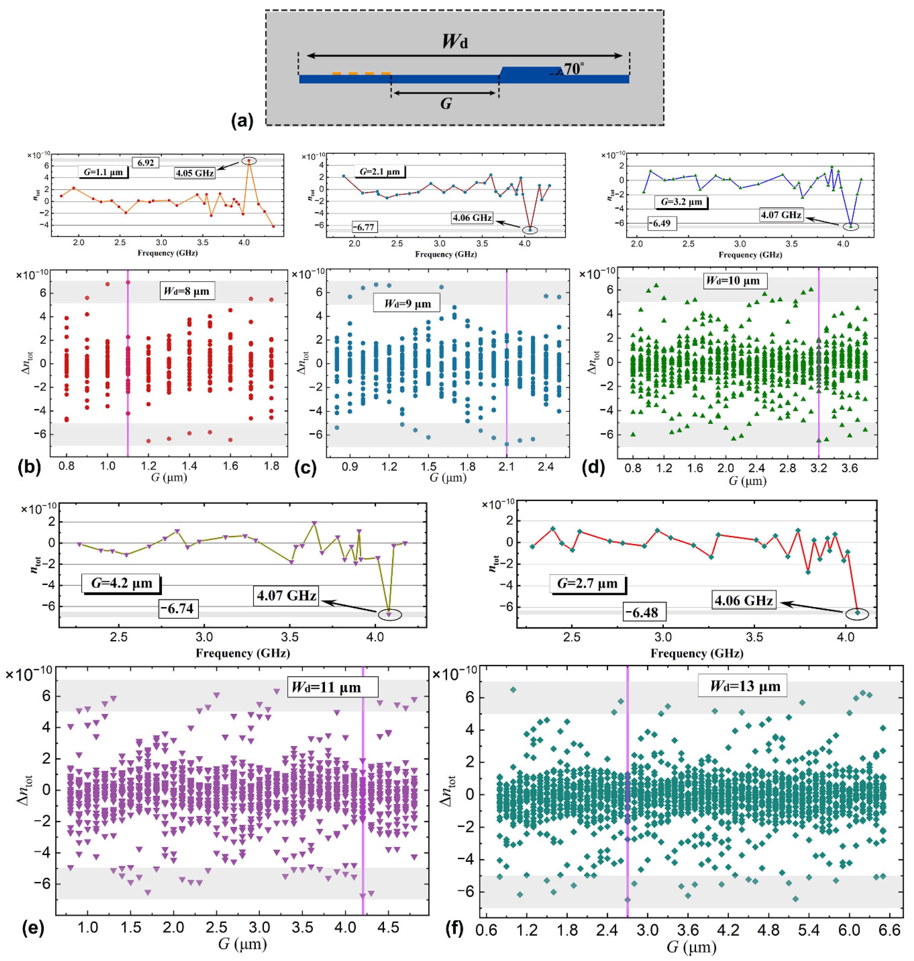
Figure 5 shows the refractive index change of the optical waveguide
as a function of the gap width
G between the optical waveguide and IDT for different widths
Wd of the acoustic resonator. The multimode waveguide width is still fixed to
w = 2.1 μm and we choose
Wd = 8, 9, 10, 11, and 13 μm. From the results, we can always find the maximum value of
for different widths of the acoustic resonator by tuning the gap width
G, and the obtained maximum values of
are all higher than
for a single phonon. The observations indicate that the field distribution of the acoustic resonator mode is closely related to the acoustic resonator width, and we need to reoptimize the position of the multimode waveguide on the TFLN for different widths
Wd in order to obtain the highest AOI, which corresponds to the maximum value of
. Moreover, through additional calculations using different acoustic resonator widths, we find that the maximum value of
can still be increased slightly if the width
Wd is further decreased. For example, the maximum value of
can be even higher than
for a single phonon if
Wd is less than 8 μm. However, such a small acoustic resonator width will lead to a decrease in the gap width between the optical waveguide and IDT, which will then increase the metal absorption loss of the AOM. From the above calculations, we determine the key cross-sectional dimension of the proposed AOM including the gap width
G, multimode waveguide width
w, and acoustic resonator width
Wd, where the AOM length along the
y-direction is set as 100 μm since the BOX layer below the AOM region needs to be removed [
33,
34]. In summary, the structural parameters of the proposed AOM can be obtained with higher AOI effect working at the higher-order TE
1 mode when compared with that working at the fundamental TE
0 mode.
Another key component of the proposed scheme is the mode converter, which realizes the conversion between the TE
0 and TE
1 mode efficiently. The mode converter is implemented by the asymmetrical directional coupler (ADC) shown in
Figure 1c. From the ADC theory, the required mode conversion can be achieved via evanescent coupling under the phase matching condition [
41,
42]. To achieve phase matching, we calculate the mode features of the TFLN optical waveguide and make the effective index of the TE
0 mode of the single mode waveguide match with that of the TE
1 mode of the multimode waveguide. The optimized results are the single mode waveguide width
w1 = 870 nm, multimode waveguide width
w = 2.1 μm, and gap width between the two waveguides
d = 330 nm. The working wavelength is
λ = 1.55 μm. Then we conduct transmission analyses to determine the optimum coupling length
LC [
43], which can be found in
Figure 6. It is noted that the highest mode transmission from the input TE
0 to output TE
1 mode is nearly 0.98 (normalized to the input power) corresponding to the coupling length
LC = 52 μm as shown in
Figure 6a. We note that the mode transmission is still higher than 0.95 even if
LC changes from 46 to 61 μm, thus relaxing the fabrication tolerance of the TFLN waveguide. The transmission wavelength spectrum of the mode converter is also analyzed. From
Figure 6b, the bandwidth is 123 nm for transmission higher than 0.95 (202 nm for transmission higher than 0.90). The large bandwidth can be utilized for broadband AOMs.
Figure 6c shows the field evolution through the whole conversion region from the input TE
0 mode to the converted TE
1 mode and then to the output TE
0 mode, where the generated TE
1 mode is used for the AOM. The mode patterns of the input TE
0 mode and the converted TE
1 mode are also shown in the insets. We find that the converted TE
1 mode has a high mode purity and low mode crosstalk, contributing to the efficient operation of the AOM working at the higher-order TE
1 mode. In summary, the key structures of the AOM and the mode converter have been obtained. The rest are typical MZI structure shown in
Figure 1a, the waveguide width of which is 870 nm.
4. Discussion
The device fabrication process can be divided into three steps; they are (1) define the TFLN waveguide structure, (2) fabricate the IDT electrode on the TFLN, and (3) open the acoustic resonator slot and remove the BOX layer below the AOM region. We can start from the X-cut TFLN wafer with a 600 nm-thick top LN layer. First, the designed optical waveguide structure of the AOM is patterned and etched on the TFLN wafer using E-beam lithography (EBL) and reactive ion etching (RIE) [
2,
3,
4,
5,
25], where the waveguide widths (
w = 2.1 μm,
w1 = 870 nm), gap (
d = 330 nm), and etching depth (
h1 = 300 nm) should be well controlled. Second, we use typical metal lift-off process to fabricate the IDT electrode [
2,
3,
4,
5,
25], where the electrode width (
a = 300 nm), gap (
b = 300 nm), and thickness (100 nm) need to be satisfied. Third, two rectangular slots on both sides of the AOM are etched on the slab layer with etching depth
h2 = 300 nm to form the acoustic resonator. Finally, we employ BOX etchant contact with the BOX layer and then remove it through two completely etched slots of the TFLN layer [
33,
34]. For these fabrication steps, we calculated the refractive index change of the optical waveguide
as functions of the IDT electrode thickness and waveguide etching depth
h1. We note that no obvious variation of
is observed as the IDT electrode thickness changes from 80 to 120 nm. In contrast, the waveguide etching depth variation has a stronger effect on
since it is directly related to the mode features of the generated SAW and the optical waveguide, leading to variation of the AOI effect. Therefore, the waveguide etching depth (
h1 = 300 nm) should be carefully controlled during device fabrication process.
Finally, we calculate the key modulation parameter
VπL for the proposed device due to refractive index change of the optical waveguide where Equation (7) is used to estimate the value. The AOM length along the
y-direction is chosen to be 100 μm and the beam length of the MZI structure is 500 μm. The typical Q factor of the acoustic resonator
= 2000,
and
= 0.15 (from experimental results) are used in the following calculations [
26].
Table 1 lists the calculation results at the TE
0 and TE
1 modes. The value of
is chosen as the maximum one generated by the specific acoustic mode frequency chosen from various acoustic mode frequencies for every device structure mentioned above. We find that the use of the higher-order TE
1 mode reduces the key modulation parameter
VπL for the proposed AOM. The minimum value
VπL is ~0.0084 V·cm, which is obviously lower than previous reports [
25,
26,
27,
28,
29].
Figure 7 shows the refractive index change
of the waveguide versus the slant angle of the TFLN waveguide sidewall. Other waveguide parameters are the same as that in
Figure 3b, where
G = 3.5 μm. Note that the allowable slant angle can be varied from 64° to 70°, while keeping
higer than
for a single phonon. Such relatively large tolerance is useful in the etching process of the TFLN waveguide. Thus, the AOI effect is enhanced by using the higher-order TE
1 mode, leading to the performance improvement of on-chip AOM.

 ,
, 


