Article

Y-Shaped Demultiplexer Photonic Circuits Based on Detuned Stubs: Application to Radiofrequency Domain

by
Abdelkader Mouadili
1,
Soufyane Khattou
2,
Madiha Amrani
2,
El Houssaine El Boudouti
2,
Noureddine Fettouhi
3,
Abdelkrim Talbi
4,
Abdellatif Akjouj
5 and
Bahram Djafari-Rouhani
5,*
1
Laboratoire Matériaux, Energie et Contrôle Système, Département de Physique, Faculté des Sciences et Techniques de Mohammedia, Université Hassan II, Casablanca 28806, Morocco
2
Laboratoire de Physique de la Matière et du Rayonnement, Département de Physique, Faculté des Sciences, Université Mohammed I, Oujda 60000, Morocco
3
ESMAR, Département de Physique, Faculté des Sciences, Université Mohammed V, Rabat 10000, Morocco
4
Université Lille, CNRS, Centrale Lille, Université Polytechnique Hauts-de-France, UMR 8520-IEMN, LIA LICS, F-59000 Lille, France
5
Département de Physique, Université de Lille, Institut d’Electronique, de Microélectronique et de Nanotechnologie (IEMN), UMR CNRS 8520, 59655 Villeneuve d’Ascq, France
*
Author to whom correspondence should be addressed.
Photonics 2021, 8(9), 386; https://doi.org/10.3390/photonics8090386
Submission received: 29 June 2021 / Revised: 6 August 2021 / Accepted: 8 September 2021 / Published: 11 September 2021

Abstract

:
We present a theoretical and experimental study of photonic demultiplexers based on detuned stubs. The demultiplexers consist of Y-shaped structures with one input line and two output lines. Two different types of structures are proposed to achieve a selective transfer of a single mode in one output line without disturbing the second one. (i) In the first platform each output contains two different stubs attached at two different sites (U-shaped resonators). We derive in closed form the geometrical parameters of the stubs to achieve a selected frequency in each line while keeping the other line unaffected. The frequency selection can be made on the basis of two different mechanisms, namely a Fano or an electromagnetic induced transparency (EIT) resonance. Consequently, different demultiplexing schemes can be designed by a combination of the two mechanisms, such as Fano-Fano, Fano-EIT or EIT-EIT. In particular, the width of the Fano or EIT resonances can become zero for an appropriate choice of the stubs’ lengths, giving rise to trapped modes also called bound in continuum states (BICs) with infinite quality factors. We also show that the crosstalk between the two outputs can reach minimum values around −45 dB. (ii) In the second platform, each output line contains a photonic comb with a defect stub. The latter is appropriately designed to filter one or a few frequencies in the bandgap of the photonic comb. The analytical calculations are performed with the help of the Green’s function method which enables us to derive the transmission and reflection coefficients as well as the density of states (DOS). These results are confirmed by experimental measurements using coaxial cables in the radio frequency domain.

1. Introduction

Wavelength selection or demultiplexing is one of the key technologies in optical telecommunications. The filtering can be based on a resonant transmission with high quality factor by introducing a cavity in a periodic structure that display localized modes in the band gap of the photonic system. This method has been the object of several works to create a demultiplexer in different dimensions 1D and 2D [1,2,3,4,5,6,7]. The width of the gap, the cavities used, and the resolution are determining factors which define the number of filtered modes. Other methods use specific resonances created by resonators inserted in a waveguide [8,9,10,11,12]. In this case, we can get peaks that can reach unity with high quality factors in the perfect materials. Two types of these resonances are electromagnetic induced transparency (EIT) [13,14] and Fano resonances [15,16]. These resonances were originally discovered for atomic systems as the consequence of destructive quantum interference phenomena between the excitation pathways to the atomic upper levels [13,14,15] and have been extended to other areas due to their interesting applications in slow light [17], data storage [18] and high performance nano-sensing [19]. Due to their strong interest, Fano and EIT phenomena are not restricted to atomic systems and have been the subject of intense studies in classical systems including photonic waveguides [20,21,22], acoustic slender tubes [23,24], plasmonic nanostructures [25,26] and metasurfaces [27]. Recently, Fano and EIT resonances have been also studied in Y-shaped demultiplexers in various areas such as photonic circuits [28], acoustic slender tubes waveguides [29,30] and plasmonic nanostructures [31,32,33]. Also, it is worth noticing that photonic demultiplexers based on 1D and 2D photonic structures have been the subject of intense studies in the last two decades due to their great interest in global communication systems [2,28,34,35,36,37]. Different mechanisms are used for designing demultiplexers based on photonic crystals such as defect waveguides [38], coupled cavities [39,40,41,42], superprisms [43], coupling and cascading photonic crystal waveguides [44], photonic crystal ring resonators [45,46], Mach-Zehnder interferometers [47], and spiral resonators [48].
Some years ago, we investigated both theoretically and experimentally the existence of Fano and EIT resonances in U-shaped [21] photonic circuits based on coaxial cables at radio frequency domain. In this work, we consider a Y-shaped demultiplexer with an input line and two output lines, where two or periodic detuned stubs are grafted at different places along each output line. In the case of the platform based on two stubs separated by a segment with U-shape, we show that different possibilities of filtering can be realized such as: Fano resonances on both outputs, EIT resonances on both outputs or EIT resonance on one output and Fano resonance on the other output. The geometrical parameters necessary to realize each filtering are obtained analytically. The particular case where the two resonators are placed at the same position, called cross-shape structure, has been studied recently [28]. This latter system enables us to obtain only EIT-EIT resonances. In order to overcome this constraint about the appropriate choice of the lengths of the stubs and segments separating them, we propose another Y-demultiplexer platform where each output contains a periodic structure with a cavity defect. The advantage of the last structure lies in the fact that it can present large gaps where the propagation is prohibited. Then, by appropriately introducing a cavity (stub defect) along each output, one can filter different frequencies inside the gap of the corresponding circuit.
This paper is organized as follows: In Section 2, we study the demultiplexer based on EIT and Fano resonances introduced by U-shaped resonators. First we give the method of calculation of transmission and reflection coefficients based on the Green’s function method [49,50] as well as some numerical results with an experimental validation for Fano-Fano demultiplexing. The other possibilities of demultiplexing such as EIT-EIT and EIT-Fano are given in the Supplementary material. In Section 3, we give the analytical calculation of the dispersion relations, transmission and reflection coefficients through a demultiplexer made of two photonic circuits in a Y-shaped form, with numerical and experimental realizations by coaxial cables. In addition, we study the performance and efficiency of these demultiplexers through an analysis of the crosstalk and local density of states (LDOS) for some filtered modes. In Section 4, we summarize and conclude the main results of this work.

2. Demultiplexer Based on U-Shaped Resonators

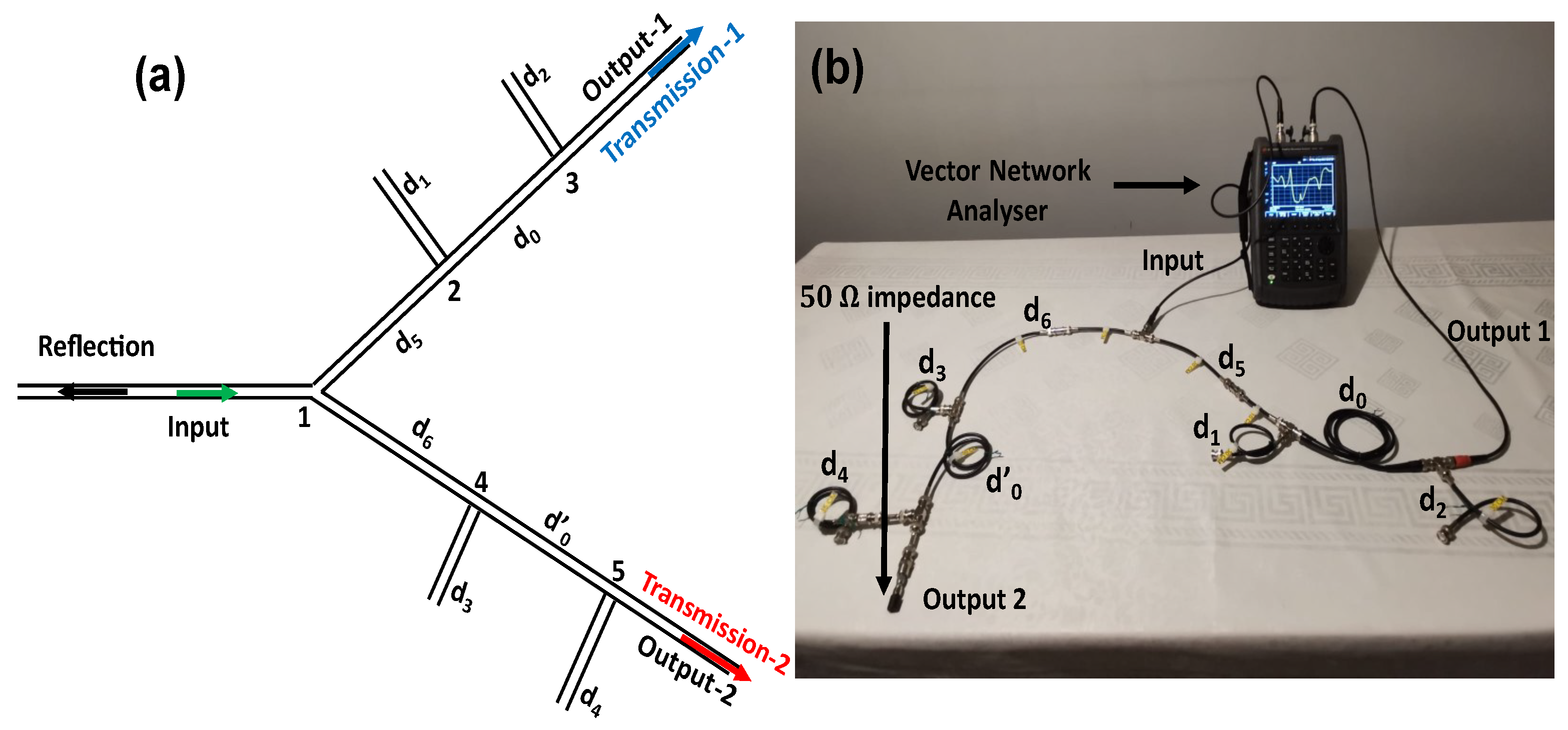
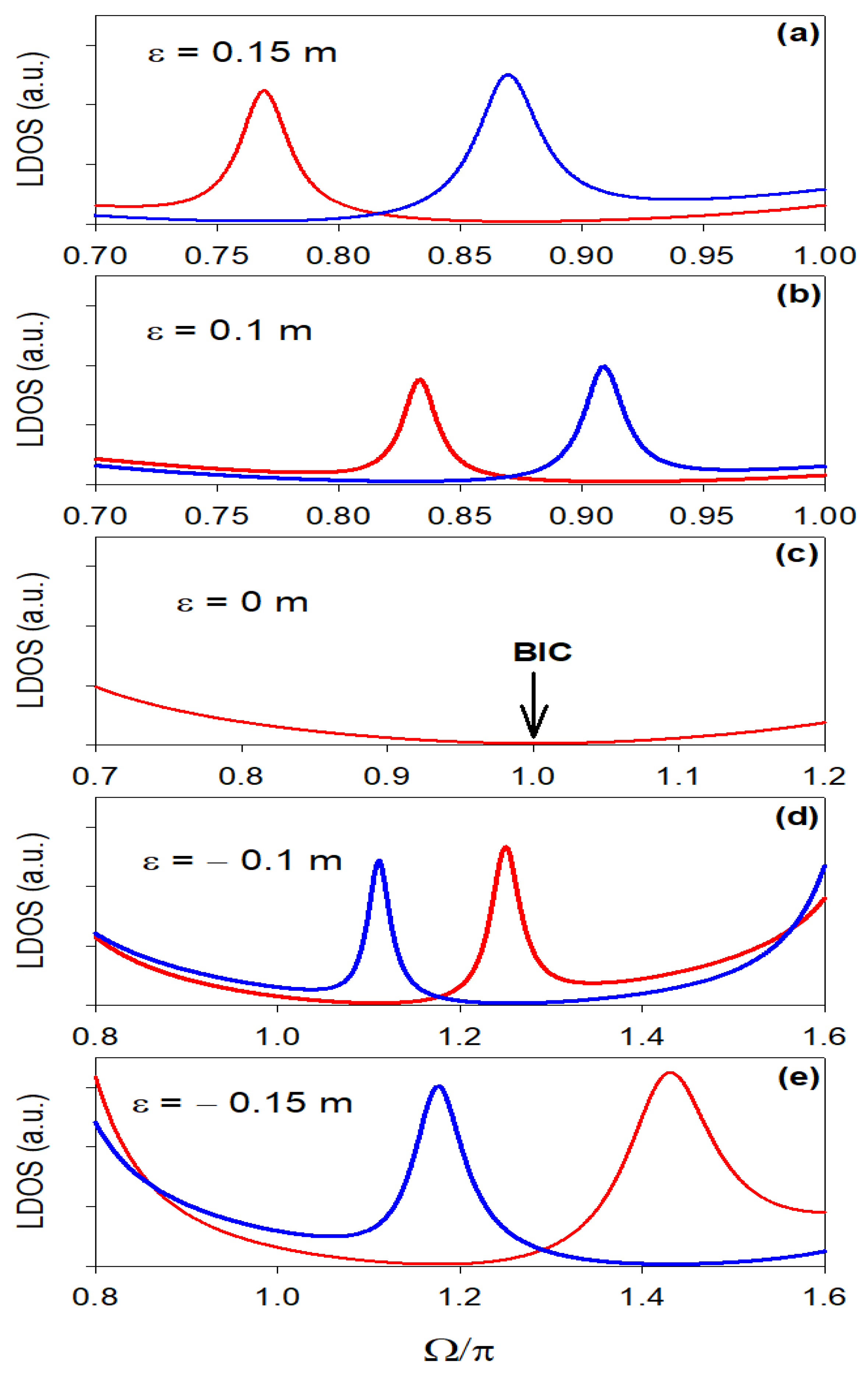
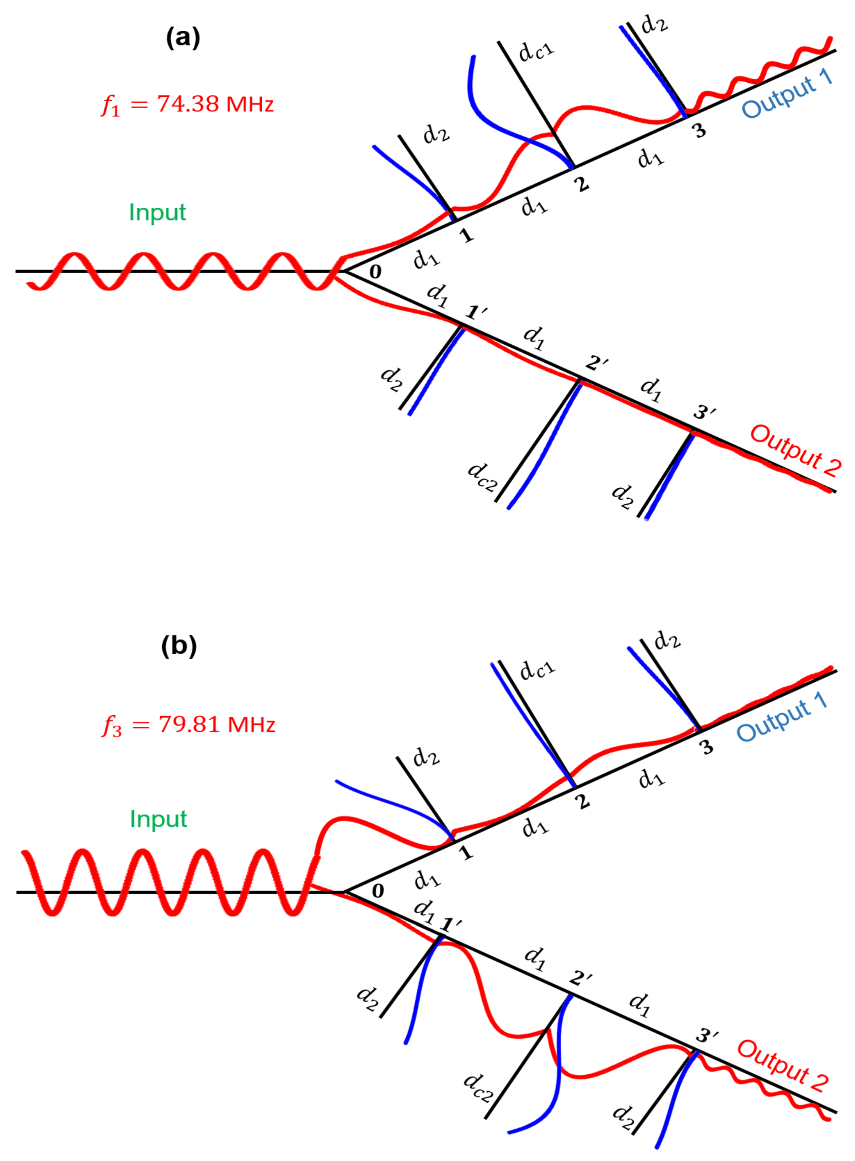
2.1. Theoretical Approach

It has been demonstrated [21] that a simple U-shaped structure made of two resonators of lengths d 1 and d 2 separated by a segment of length d 0 , inserted inside a waveguide, may present Fano and EIT resonances. Each resonator induces its own transmission zero at specific frequencies depending on its length d i (i = 1,2). If the lengths of the two resonators d 1 and d 2 are slightly different and d 0 = d 1 + d 2 , a resonance (transparency window) falls between the two transmission zeros giving rise to an EIT resonance. In the particular case where d 0 = d 1 + d 2 , the EIT resonance appears symmetrically between the two transmission zeros, and its width depends on the detuning between the two stubs δ = d 2 d 1 . Conversely, in order to obtain a Fano resonance, the lengths of the two stubs should be taken identical and slightly different from d 0 2 (i.e., d 1 = d 2 d 0 2 ). In the particular case where d 1 = d 2 = d 0 2 , the resonance coincides with the two transmission zeros giving rise to a zero-width resonance called bound states in continuum (BIC) with an infinite quality factor [51].
In this section, we use the characteristic of the U-shaped resonators, namely Fano and EIT resonances, to design a Y-shaped demultiplexer based on the combination of the two resonances (Figure 1). The platform consists of one input line and two output lines. Each output contains a U-shaped resonator where two stubs are placed at different sites along the output line. On the first output the two stubs of lengths d 1 and d 2 are attached on two different sites separated by a segment of length d 0 . The stub of length d 1 is grafted at the site { 2 } at a distance d 5 from the entrance and the stub of length d 2 is grafted at the site { 3 } at a distance d 5 + d 0 from the entrance. Likewise, the second output contains two lateral stubs of lengths d 3 and d 4 separated by a segment of length d 0 . These two stubs are placed respectively at the sites { 4 } and { 5 } at a distance d 6 and d 6 + d 0 from the input line. All waveguides are coaxial cables constituted by the same dielectric permittivity ε d and characterized by the same impedance Z.
In order to calculate the transmission and reflection coefficients through the U-shaped demultiplexer depicted in Figure 1, we need the Green’s function elements in the space of interfaces of the whole system (Figure 1). The details of the analytical calculations are given in Supplementary material SM1. Using the Green’s function method [49,50], the Green’s function of the whole system can be obtained by a linear superposition of the inverse Green’s functions of its elementary constituents, namely
g 1 ( M M ) = ω Z C 5 S 5 + C 6 S 6 j 1 S 5 0 1 S 6 0 1 S 5 C 5 S 5 + C 0 S 0 + S 1 C 1 1 S 0 0 0 0 1 S 0 C 0 S 0 + S 2 C 2 j 0 0 1 S 6 0 0 C 6 S 6 + C 0 S 0 + S 3 C 3 1 S 0 0 0 0 1 S 0 C 0 S 0 + S 4 C 4 j
where C i = cos ( k d i ) , S i = sin ( k d i ) ( i = 0 , 0 , 1 , 2 , 3 , 4 , 5 , 6 ) and j = 1 . k = ω ε d c is the wave vector of the incident wave, ω is the pulsation, ε d the dielectric permittivity of the waveguides and c the speed of light in vacuum.
Let us consider an incident wave U ( x ) = e j k x launched in the left semi-infinite waveguide (Figure 1). The amplitude of the reflected wave in the semi-infinite waveguide at the input of the demultiplexer is defined by [49,50]
r = 1 ( 2 j ω / Z ) g ( 1 , 1 ) ,
where g(1,1) is the Green’s function at the site { 1 } at the entrance of the demultiplexer (Figure 1). The amplitudes of the transmitted waves in the two semi-infinite outputs 1 and 2 (Figure 1) are given respectively by
t 1 = ( 2 j ω / Z ) g ( 1 , 3 ) ,
and
t 2 = ( 2 j ω / Z ) g ( 1 , 5 ) ,
where g(1,3) (g(1,5)) is the Green’s function between the sites { 1 } and { 3 } ( { 1 } and { 5 } ) along the first (second) output of the demultiplexer (Figure 1).
The analytical expressions of the transmission and reflection amplitudes are quite complicated. Thus, we give only the conditions that should be satisfied by all the lengths of the waveguides in order to realize an efficient demultiplexing. In addition, in the next section we will distinguish between three different possibilities of demultiplexing depending on the choice of the lengths of the stubs on each output such as Fano-Fano, Fano-EIT or EIT-EIT resonances on both output lines. However, in order to shorten the length of the paper, we will give the details of the results only in the case of Fano-Fano resonances and postpone the results of EIT-EIT and EIT-Fano to supplementary materials (SM2 and SM3).

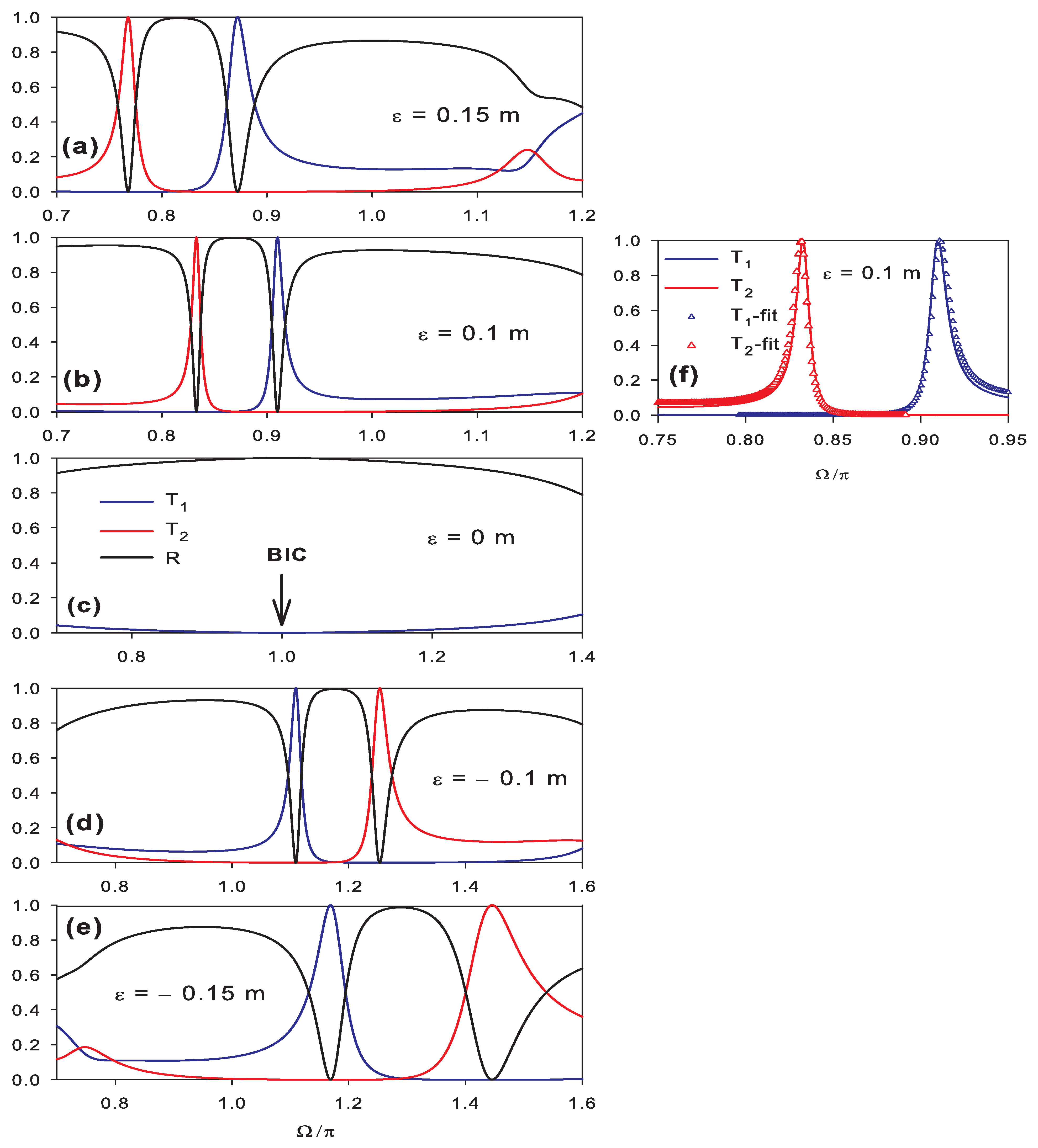
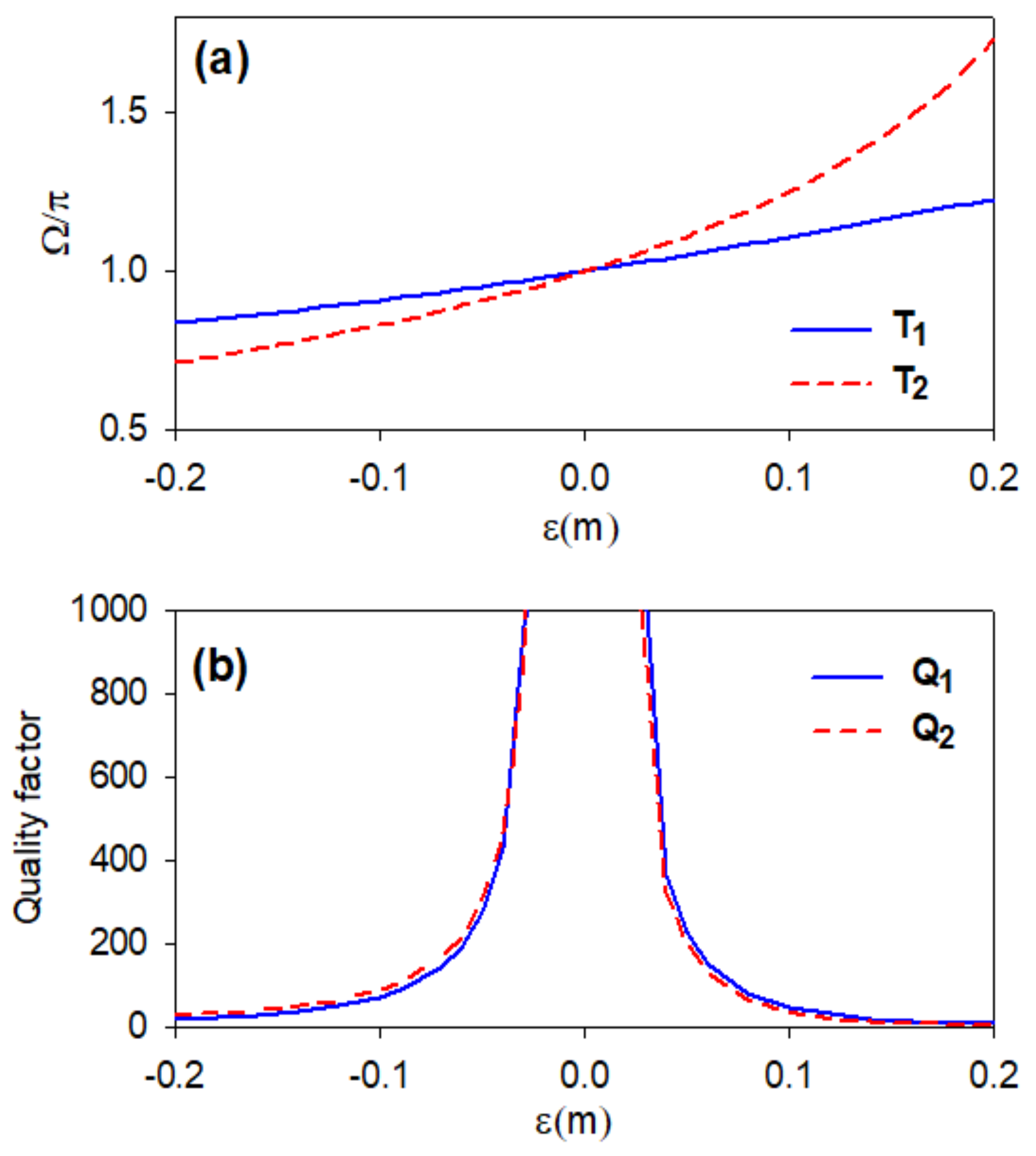
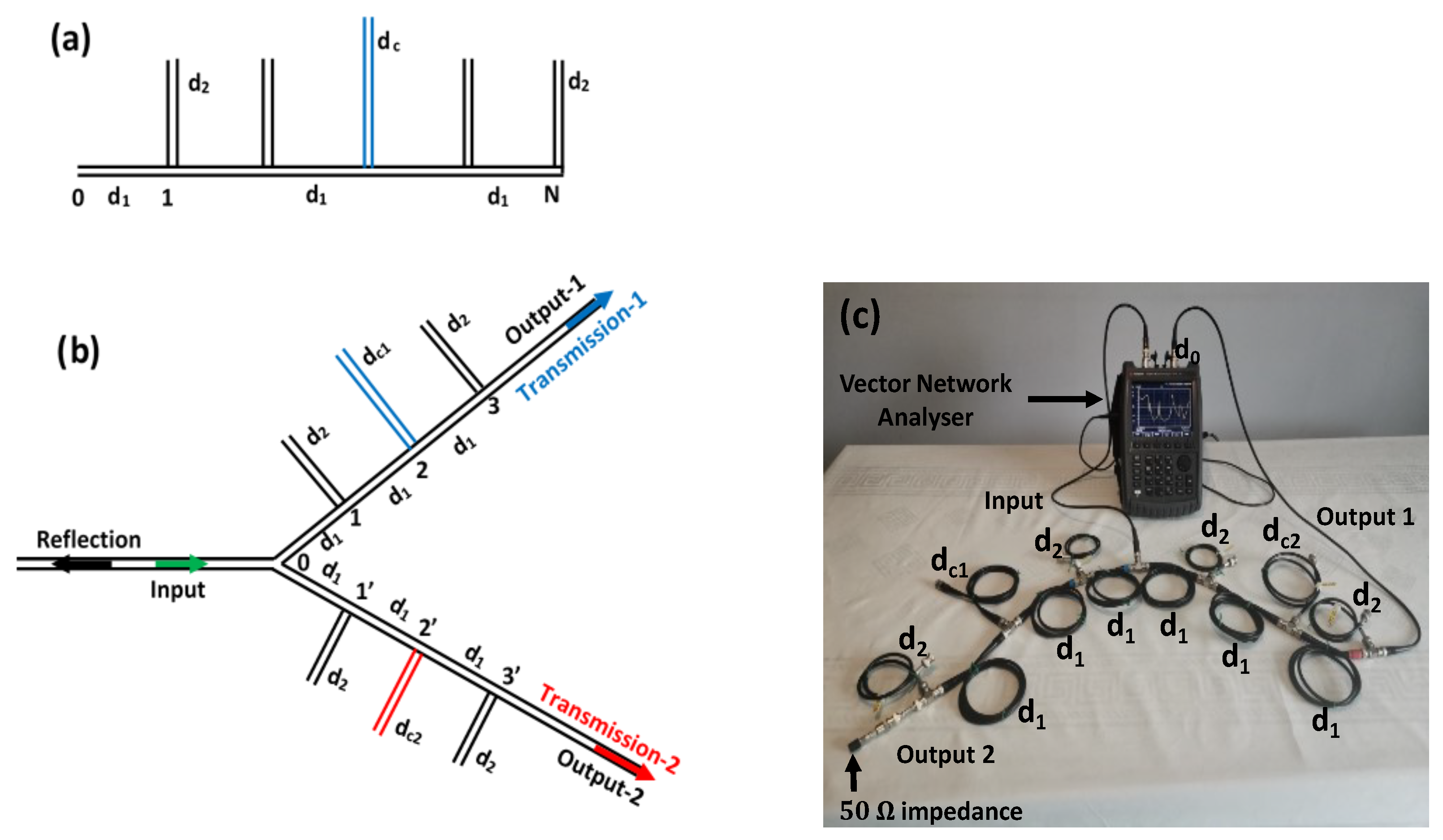
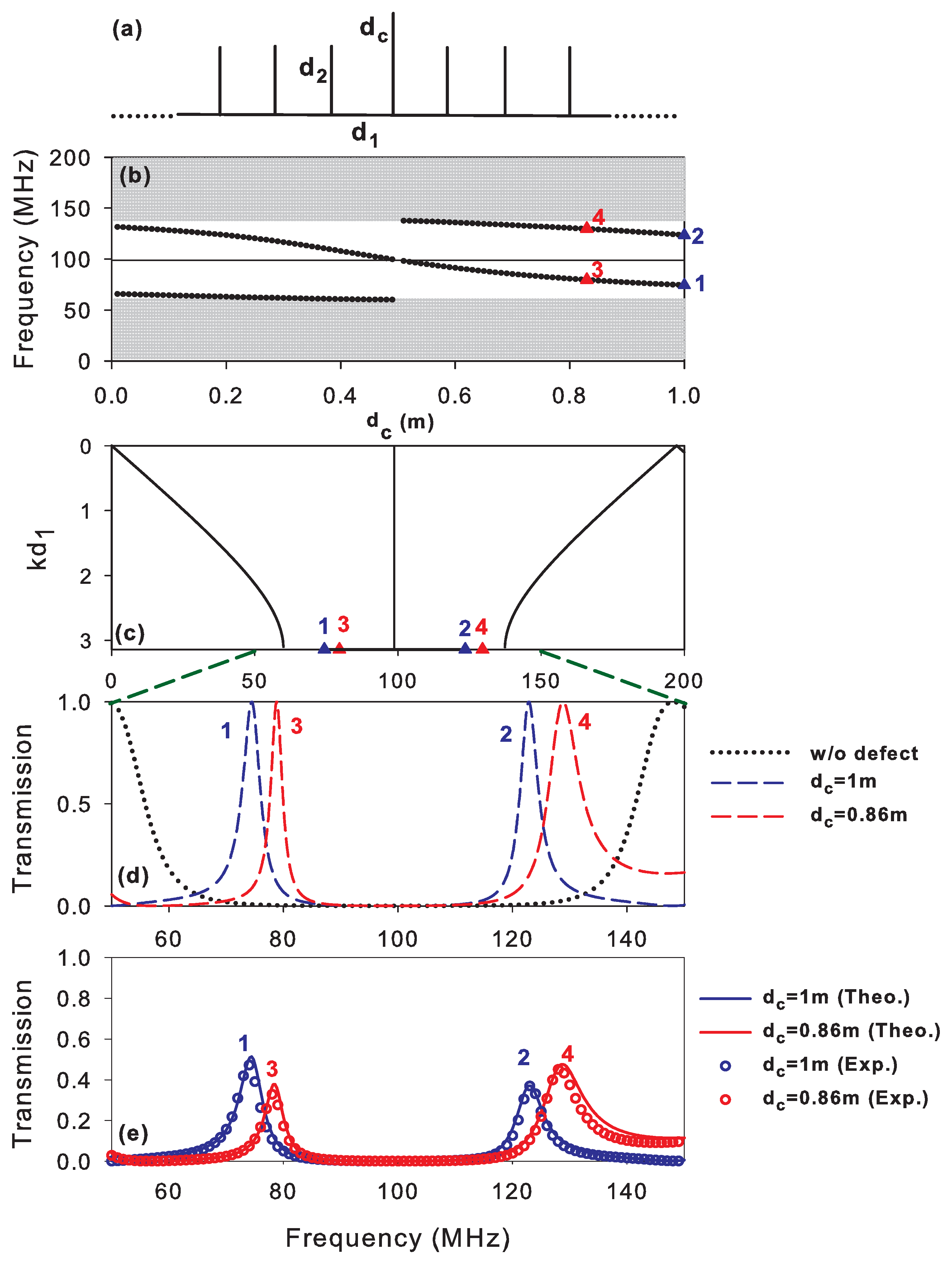
2.2. Numerical and Experimental Results

As mentioned previously, the U-shaped resonators can give rise to EIT and Fano resonances. These resonances are respectively characterized by the existence of a resonance between two transmission zeros or by a resonance lying in the vicinity of a transmission zero. Based on the geometrical parameters, we are able to precise the system parameters to achieve a complete filtering in one output without disturbing the other output. As it was demonstrated earlier [21], in order to obtain a Fano resonance on both outputs, we should take the lengths of the stubs along the first output identical and slightly different from d 0 2 (i.e., d 1 = d 2 = d 0 2 ε ) and the two stubs along the second outputs should be chosen different from d 0 2 (i.e., d 3 = d 4 = d 0 2 + ε ). These two conditions ensure that we obtain Fano resonances on both outputs.
Now, we are able to specify the system parameters to realize a full transmission in one output keeping the other one unaffected. Indeed, in order to realize a complete transmission in the first output ( T 1 = 1 ), we have to cancel simultaneously the transmission in the second output and the reflection along the input (i.e., T 2 = R = 0 ). The expressions of t 2 (Equation (4)) and r (Equation (2)) are quite complicated, so by analogy with the analytical demonstrations performed in the case of simple U-resonator [21], to cancel both T 2 and R (i.e., T 2 = R = 0 ) at specific frequencies, one should have C 3 = 0 or C 4 = 0 and C 6 = 0 . Similarly in the second output, the two stubs d 3 and d 4 induce their own transmission zeros, these occur when C 3 = 0 or C 4 = 0 [28]. In a lossless system, the transmission zeros are given respectively by k d 3 = ( 2 m 3 + 1 ) π 2 or k d 4 = ( 2 m 4 + 1 ) π 2 where m 3 and m 4 are two integers. The position of the Fano resonance in the first output is fixed by sin ( k ( d 0 + ε ) ) = 0 (i.e., k ( d 0 + ε ) = m π ) where m is an integer. Likewise, in order to realize T 2 = 1 , T 1 = 0 , R = 0 , one should satisfy C 1 = 0 or C 2 = 0 (i.e., k d 1 = ( 2 m 1 + 1 ) π 2 or k d 2 = ( 2 m 2 + 1 ) π 2 where m 1 and m 2 are two integers) and C 5 = 0 . The position of the Fano resonance in the second output is fixed by s i n ( k ( d 0 ε ) ) = 0 (i.e., k ( d 0 ε ) = m π ), where m is a non-zero integer.
From the above conditions, one can derive that for the first order demultiplexing (i.e., m 1 = m 2 = m 3 = m 4 = 0 and m = m = 1 ), the lengths of the eight segments should be taken as follows:
d 1 = d 2 = d 0 2 + ε ,
d 3 = d 4 = d 0 2 + ε 2 ,
d 5 = d 0 2 + ε ,
d 6 = d 0 2 + ε 2 ,
d 0 = d 0 + 3 ε .
In order to illustrate the results of the above analysis, we present in Figure 2 the variation of the transmission coefficients T 1 , T 2 along the two outputs and the reflection coefficient R along the input as a function of the dimensionless frequency Ω = ω d 0 ε d c where d 0 = d 1 + d 2 for different values of ε . One can notice that the dimensionless frequency of the Fano resonance is lower than π for positive values of ε and becomes higher than π when ε is negative.
Figure 2 shows that for different values of ε one can obtain a full transmission along the first output T 1 (blue curves) when both the transmission in the second output T 2 (red curves) and the reflection R (black curves) vanish at the same frequency (i.e, T 2 = R = 0 ). Similarly in the second output, the transmission T 2 (red curves) reaches unity when the transmission in the first output T 1 (blue curves) and the reflection R (black curves) vanish (i.e., T 1 = R = 0 ). It means that one can obtain a filtered wave in one output without perturbing the other one. The two selected resonances have a Fano-like shape, i.e., resonance lying at the vicinity of a transmission zero. Figure 2 clearly shows that the frequency of the Fano resonance varies as function of ε in the two outputs 1 and 2. However, the variation of the frequency of the resonance in output 2 (red lines) depends strongly on ε in comparison with the variation of the resonance frequency in the first output (blue lines) (see Figure 2 and Figure 3a). The other important remark concerns the order of the resonance and the transmission zeros on the same line. We can see that the Fano line shape is inverted from one resonance to another resonance (see below) in order to combine the peak of one with the zero of the other and vice-versa. For ε > 0 , the Fano resonance in the second output appears below the one in the first output (Figure 2a). As ε decreases, the two resonances approaches to each other (Figure 2b) and coincide for ε = 0 giving rise to a BIC state which is characterized by a zero-width resonance (i.e., infinite quality factor) as shown in Figure 2c. For ε < 0 , the Fano resonance in the second output becomes at the other side and appears at the right hand side of the Fano resonance in the first output (Figure 2d,e).
In order to confirm that the two filtered resonances are of Fano type, the latter should be fitted by a Fano-like expression such as [16]
T = A ( ω ω r + q Γ ) 4 ( ω ω r ) 2 + Γ 2
where A = 1 q 4 Γ 2 . ω r and Γ are the parameters that denote the position and the width of the resonance, respectively. q is the so-called Fano parameter which describes the degree of asymmetry of the resonance. An example of the results of the fitting expression (Equation (10)) is shown in Figure 2f for ε = 0.1 m (Figure 2b). The fitted results represented by open triangles fit very well the exact results presented by solid lines. From the fitted results, one can deduce that the resonance on the first output (blue curve) exhibits a Fano shape with ω r = 0.91 π , q = 12 and Γ = 0.02 π . Similar results are found for the second resonance (red curve) with ω r = 0.83 π , q = 15 and Γ = 0.015 π . Figure 3a gives the variation of the positions of the two resonances along the two outputs as a function of ε . One notes that the frequencies of the two resonances on the two outputs depend strongly on ε . This dependence appears greater in the second output (dashed line) compared to the first output (solid line). In addition, the resonance in the second output (solid line) falls below the one in the first output (dashed line) for ε > 0 , coincide with it for ε = 0 giving rise to a BIC mode, and reappears above the resonance on the first output for ε < 0 . Figure 3b shows the variation of the quality factors Q 1 (continuous line) and Q 2 (dashed line) of the two Fano resonances discussed in Figure 2 as function of ε . One can notice that the quality factors of both demultiplexed signals are almost similar and give the same behavior as a function of the parameter ε . For lower values of ε , the Q-factors reach high values around Q 1000 . However, for ε = 0 the width of the resonance vanishes for lossless system, and its Q-factor diverges towards infinity values which gives a clear signature of the existence of BIC state [51]. This mode remains confined in the U-shaped resonators and does not interact with the continuum modes associated to the semi-infinite waveguides.
In order to give a better insight about the spatial localization of the different modes that can be selected or stopped by the U-shaped demultiplexer, we have presented in Figure 4 the square modulus of the electric field along the two outputs of the system for the two Fano resonances discussed in Figure 2b for ε = 0.1 m. Figure 4a shows that the first Fano resonance at Ω = 0.91 π corresponds to a filtered mode along the first output, while this mode is stopped along the second output. The transfer of this mode along the output 1 can be explained by the excitation of both stubs of lengths d 1 and d 2 and the segment d 0 which separate them. Its stopping along the output 2 is due to the excitation of the stationary mode of the stub of length d 3 as shown in Figure 4a. Figure 4b gives the same results as in Figure 4a but for the second Fano resonance which appears at Ω = 0.83 π (Figure 2b). The wave at this dimensionless frequency is completely transferred along the second output due to the excitation of both stubs of lengths d 3 and d 4 as well as the segment d 0 , whereas the wave is completely stopped along the first output through the excitation of the stationary mode of the stub of length d 1 . These results show that one can achieve a good filtering in one output keeping the other output unaffected by appropriately choosing the lengths of the different segments and stubs along the two outputs.
In order to give an experimental validation of the above theoretical results, we performed an experiment using standard coaxial cables in the radio frequency domain [52]. The experiment is carried out using coaxial cables and a vector network analyzer. The experimental setup is shown in Figure 1b. The cables are characterized by the same characteristic impedance and permittivity. The coaxial cable is RG-58/U with an impedance equal to Z = 52 Ω . The core and sheath of the cables are separated by a polyethylene layer characterized by a dielectric permittivity ε = 2.3 which corresponds to a nominal propagation speed of the order of 0.66c. The connection between the cables is made by BNC connectors in the form I or T or cross. The elements of the scattering matrix are measured in the interval 1–200 MHz by the vector network analyzer Agilent PNA-X N5242A type. The number of acquisition points is adjusted to 5000 points with a step of 100 Hz. The acquisition results include both the magnitude and the phase of transmission ( S 12 = S 21 ) and reflection ( S 11 = S 22 ). The attenuation inside the coaxial cables was simulated by introducing a complex dielectric constant ( ε + j ε ) . The attenuation coefficient α can be expressed as α = ε ω / c ε . On the other hand, the attenuation specification data supplied by the manufacturer of the coaxial cables in the frequency range of 10 to 200 MHz can be approximately fitted with the expression ln ( α ) = γ + η ln ( ω ) , where γ and η are two constants. From this fitting procedure, a useful expression for ε as a function of frequency can be obtained under the form ε = ( f f 0 ) 0.5 where the frequency f is expressed in Hertz and f 0 = 9200 Hz. During the measurement, the input of the demultiplexer is connected to the analyzer and an output of the demultiplexer is connected to the other input of the analyzer, while the second output of the demultiplexer is blocked by a cap of 50 Ω . The ends of the stubs (cables connected vertically to the guides) are open with free boundary conditions i.e., vanishing magnetic field (perfect magnetic conductor) at the end of the stubs. Since the section of the cables is small enough compared to their lengths, the monomode propagation is verified.
Figure 5 gives the theoretical (continuous lines) and experimental (open circles) transmission and reflection coefficients as a function of the frequency along the output 1 (blue curves) and the output 2 (red curves). The reflection coefficient is given by the black curves. The lengths of the different cables are chosen to realize Fano resonances on both outputs such as: d 0 = 1 m, d 1 = d 2 = 0.35 m, d 5 = d 2 , d 3 = d 4 = 0.425 m, d 6 = d 3 and d 0 = 0.55 m which are very close to the conditions required in Equations (5)–(9) with ε = 0.15 m. The experimental results are in good agreement with the theoretical ones. The amplitudes of the resonances do not reach unity due to the attenuation in the cables. One can see that when the amplitude is maximal in one output line, it becomes minimal in the other output line as well as in the input line.
Another quantity that can characterize the demultiplexer is the crosstalk which is defined as the ratio between the power in the interested channel P i c and the power in the other channel P o c [53]
C = 10 log P o c P i c .
In Figure 5, the crosstalk for output 1 compared to output 2 for the filtered frequency 112.51 MHz is about −45.3 dB, whereas the crosstalk is about −45.41 dB for output 2 compared to output 1 for the filtered frequency 142.73 MHz. Let us mention that for lossless system, the wave is completely transferred along one output (T = 1) and stopped (T = 0) on the other output, and therefore the crosstalk in this case tends to infinity. In other words, the two outputs do not communicate with each other. However, for lossy systems as it is the case in Figure 5, the crosstalk shows finite values. In Table 1, we give a comparison of crosstalk values with previous works of demultiplexers based on photonic crystals with two outputs:
The results presented in Table 1 show that the proposed demultiplexer has better performance in comparison with previous works and has a good potential to be used for communication application in WDM systems. Indeed, the advantage of our design lies in the possibility to coincide a maximum of transmission in one line with almost zero transmission in the second line; this is a characterestic property of Fano resonances.
In addition to the results of the reflection and transmission amplitudes presented in Figure 2, one can display the LDOS of the electromagnetic wave at specific points along the two outputs. From the imaginary part of the interface Green’s function elements (Equation (1)), one can derive the LDOS at the points { 2 } and { 3 } along the first output and at the points { 4 } and { 5 } along the second outputs, as follows
n 1 ( ω ) = 2 ω π c 2 I m [ g ( 2 , 2 ) + g ( 3 , 3 ) ]
and
n 2 ( ω ) = 2 ω π c 2 I m [ g ( 4 , 4 ) + g ( 5 , 5 ) ] ,
where g ( i , i ) is the Green’s function elements at the interface { i } (i = 2,3,4,5).
Figure 6 presents the LDOS at specific points along the first output (blue curves) and second output (red curves) for the same values of ε as in Figure 2. The behavior of Fano resonances discussed in Figure 2 appear as well defined peak in LDOS. Figure 6 shows that as ε increases, both the width and the intensity of the peaks decreases. It can be seen that both peaks depend strongly on the parameter ε . Also, the first peak which corresponds to the first Fano resonance appears above the second one for ε > 0 (Figure 6a,b), and below the second peak for ε < 0 (Figure 6d,e). For ε = 0 , the LDOS gives a clear signature of the BIC state as a zero-width peak (Figure 6c) despite the existence of loss in the cables. Let us mention that for lossy system, as it is the case of coaxial cables, the intensity of the resonance for ε = 0 (Figure 6c) tends to zero and its full width at half maximum (i.e., Q-factor) becomes ill-defined.
It should be mentioned that from the U-shaped resonators, one can derive another particular case called mixed demultiplexer structure. This structure can be obtained when the two stubs on one output being located at the same position (i.e., d 0 = 0 on the fist output or d 0 = 0 on the second output), while the two stubs on the other output remain separated (i.e., d 0 0 or d 0 0 ). The mixed structure may exhibit two different possibilities of demultiplexing, namely EIT-EIT resonances on both outputs or EIT resonance on one output and Fano resonance on the second one. To shorten the length of the paper, we have avoided giving these results.

3. Demultiplexer Based on Photonic Circuits with Cavities

3.1. Theoretical Approach

In this section, we present another type of a Y-demultiplexer platform based on periodic photonic circuits in presence of cavities along each output. The cavity in the middle of the photonic crystal is obtained by replacing a stub of length d 2 by a stub of length d c ( d c d 2 ) (see Figure 7). The advantage of such a system lies in the presence of large gaps induced by the photonic circuit where waves are not allowed to propagate. The photonic circuits in each output are assumed to be identical, which makes it possible to have the same regions of forbidden frequencies for both lines. Then by introducing specific defects on each line, we can filter a well-defined frequency associated with that defect, while it is rejected by the other line. Such a demultiplexer has been studied numerically in 1D comb waveguides [57] and microstrip lines [38,58,59,60]. However, to our knowledge, a detailed analytical study and an experimental realization of such a demultiplexer is lacking.
The calculation of transmission and reflection coefficients along each output line of Figure 7b first requires the calculation of the Green’s function of each finite structure (Figure 7a). The details of the analytical calculations of the inverse of the Green’s function g 1 1 ( M i M i ) of the finite structure (Figure 7a) are given in Supplementary material SM4. Indeed, the inverse of the Green’s function of the finite comb structure with cavity (Figure 7a) in the interface space M i = { 0 , N i } can be written as follows (see SM4):
g 1 1 ( M i , M i ) = A i B i B i A i ,
where A i , A i and B i are real quantities for lossless systems which are function of the geometrical parameters of the system.
In the case of the demultiplexer described in Figure 7b, each output line is formed from a finite comb structure with its own cavity of length d c i with i = 1 or 2. The inverse of the Green’s function g 2 1 ( M i , M i ) of the whole structure is obtained by the superposition of the inverses of the Green’s functions g i 1 ( M i , M i ) (Equation (14)) of each comb, namely
g 2 ( M i , M i ) 1 = F + A 1 + A 2 B 1 B 2 B 1 A 1 F 0 B 2 0 A 2 F ,
F = j ω Z is the inverse of the Green’s function of the semi-infinite waveguides surrounding each comb. Note that A i , A i and B i are real quantities for lossless systems, while F is pure imaginary.
The transmission coefficient is defined by t i = 2 F g 2 ( 1 , i ) for each line i (i = 2,3), its expression is given by:
t 1 = 2 F B 1 ( A 1 + F ) ( F + A 1 + A 2 B 1 2 A 1 + F B 2 2 A 2 + F ) ,
along the first output and
t 2 = 2 F B 2 ( A 1 + F ) ( F + A 1 + A 2 B 1 2 A 1 + F B 2 2 A 2 + F ) ,
along the second output. The reflection coefficient at the input of the system is given by r = 1 2 F g 2 ( 1 , 1 ) , or equivalently,
r = 1 + 2 F F + A 1 + A 2 B 1 2 A 1 + F B 2 2 A 2 + F .

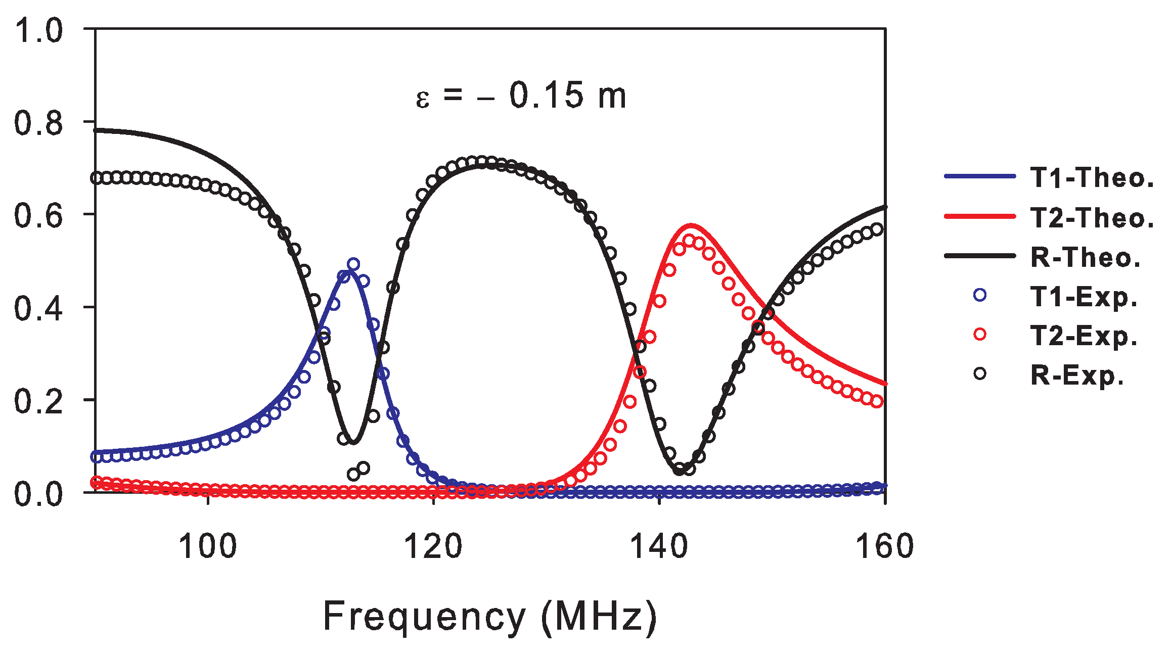
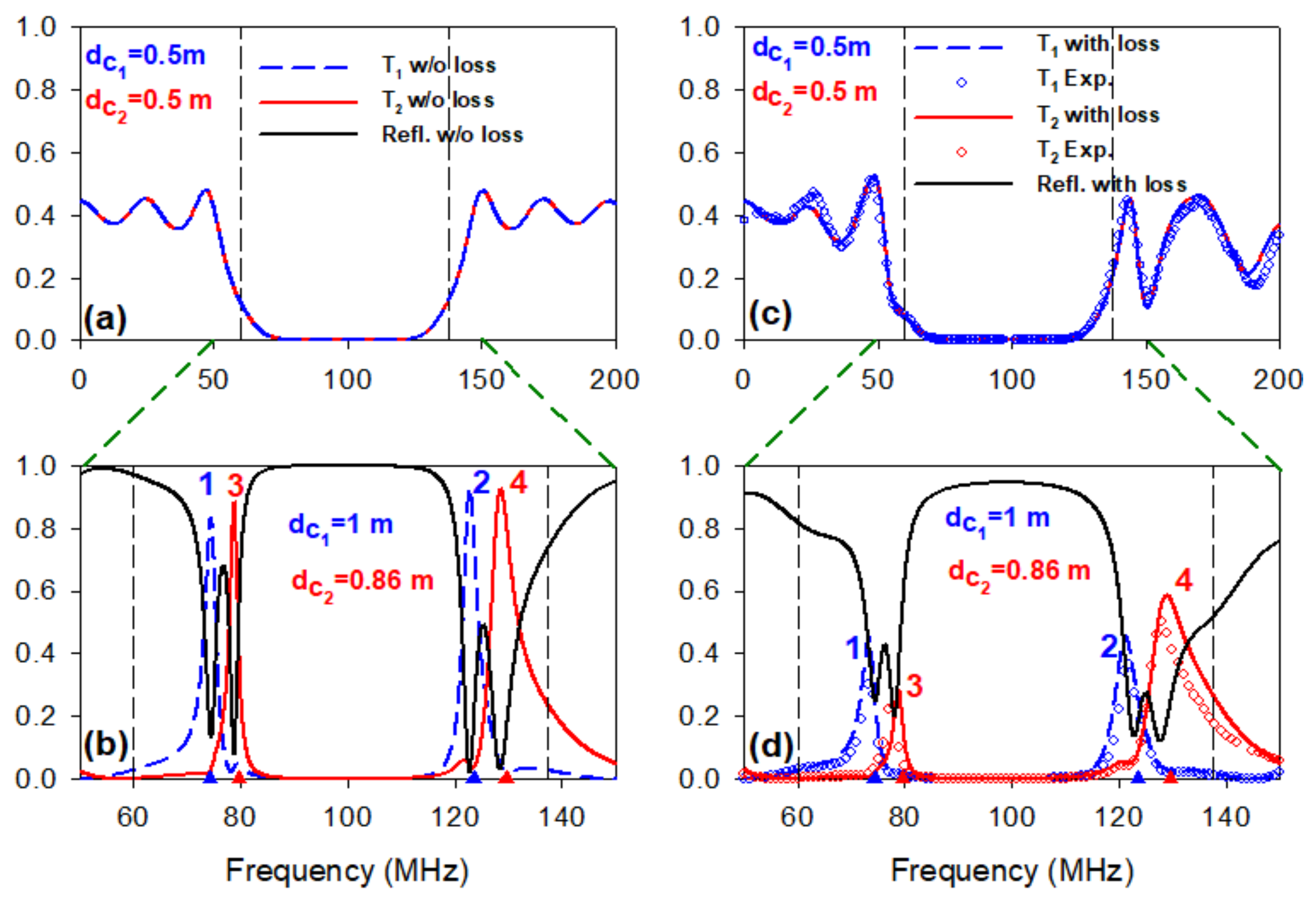
3.2. Numerical and Experimental Results

Before showing the filtered frequencies using a demultiplexer based on photonic circuits, we will first present the dispersion relation for an infinite comb structure as well as the dispersion curves of cavity modes induced by a stub defect of length d c in a periodic comb structure (Figure 7a). The dispersion relation in the case of periodic comb structure made of segments of lengths d 1 separated by stubs of length d 2 is given by [61]
cos ( k d 1 ) = C 1 1 2 S 1 S 2 C 2 ,
where C i = cos ( k d i ) , S i = sin ( k d i ) (i = 1,2) and k is the Bloch wave vector. Similarly, the dispersion relation of an infinite comb structure with a defect stub of length d c is given by [61]
S c C c 2 S 1 2 S 1 S 2 S c C 2 C c + 2 C 1 S 2 C 2 + 2 S 1 = 0
together with the condition
C 1 S 1 S c 2 C c < 1 ,
where C c = cos ( k d c ) and S c = sin ( k d c ) .
The latter condition ensures that the waves are evanescent in the photonic circuit far from the stub defect.
Figure 8b gives the dispersion curves, i.e., allowed bands (shaded areas) and the forbidden bands (white areas) of an infinite comb structure formed by stubs of length d 2 = 0.5 m periodically separated by segments of length d 1 = 1 m (Figure 8a). One can notice the existence of a flat band with zero-width at f = 98.68 MHz (i.e., ω d 2 ε d c = π 2 ) due to the choice of cable lengths d 2 = d 1 2 . The choice of such commensurable lengths enables us to get a large gap (≃80 MHz) around 100 MHz. If d 2 is chosen substantially different from d 1 2 , the flat band becomes wide (see Ref. [61]). The allowed bands are obtained from | cos ( k d 1 ) | 1 (i.e., k real), while the forbidden bands (gaps) are given by | cos ( k d 1 ) | > 1 . Inside the gaps, we have presented by dotted lines the cavity modes induced by the stub of length d c inserted in the periodic comb structure. These modes are obtained from Equations (20) and (21). The cavity modes depend on the length of the stub defect d c . One can see that the frequencies of the existing modes decrease as d c increases. Also, except for d c = d 2 = 0.5 m, one can obtain for a given value of d c two modes at two different frequencies in the region 0 d c 1 m (Figure 8b).
Figure 8c gives the dispersion curves (frequency versus the dimensionless Bloch wave vector k d 1 ) of the infinite periodic comb structure. Inside the first two gaps, we have presented the positions of the modes labeled 1, 2, 3 and 4 in Figure 8b. These modes 1 and 2 (3 and 4) are induced by the cavity of length d c = 1 m ( d c = 0.86 m). Figure 8d shows the transmission coefficient through a finite photonic crystal formed by three stubs of lengths d 2 separated by segments of length d 1 (Figure 7a). The stub in the middle of the photonic crystal may be chosen different from the other stubs of the periodic circuit ( d c d 2 ) . The black dotted lines represent the transmission through a finite photonic circuit without defect (i.e., d c 1 = d c 2 = d 2 = 0.5 m). The transmission spectrum shows a broad gap around the frequency region [60–137] MHz which coincides well with the gap presented by the dispersion curves (Figure 8c) and this despite the limited number of stubs (N = 3) constituting the finite photonic crystal. In addition, one can notice that the flat band of the infinite crystal around f = 98.90 MHz coincides with the transmission zeros of the finite crystal (Figure 8d). This frequency is given by cos ( ω d 2 ε d c ) = 0 (i.e., ω d 2 ε d c = ( 2 n + 1 ) π 2 where n is an integer), and the first mode corresponds to n = 0 at f = 98.90 MHz. The dashed lines in Figure 8d give the transmission in the case of two different defect stubs introduced in the photonic comb. The two transmission peaks within the gap coincide perfectly with the modes marked 1, 2, 3 and 4 in Figure 8b,c of the infinite crystal (indicated by red and blue triangles). The advantage of the photonic circuit is the existence of a large frequency domain that can be filtered by detuning the length of the stub cavities while remaining in the gap. Figure 8e shows an experimental validation of the theoretical results presented in Figure 8d. The solid lines in Figure 8e give the theoretical results in presence of loss, whereas open circles represent the experimental results. Both results show a good agreement. The amplitudes of the two resonances do not reach unity due to the loss in the cables.
Figure 9 represents the transmission spectra through the two outputs of the demutiplexer based on photonic circuits with or without cavities (Figure 7b). Each output is formed of a finite photonic circuit composed of three stubs of lengths d 2 separated by segments of length d 1 . Figure 9a gives the transmission in the two outputs where the two photonic circuits are chosen identical and without defects (i.e., d c 1 = d c 2 = d 2 = 0.5 m). Therefore, the two photonic circuits will exhibit the same forbidden bands (gaps) as shown in Figure 8b,c. In addition, one can notice that the amplitude of the transmission does not exceed 0.5 since the incident signal is divided between the two output lines. The advantage of the demultiplexer based on photonic circuits is the existence of a large gap where any frequency can not propagate and by changing appropriately the length of the cavities, one can filter two closed frequencies inside the gaps. Figure 9b gives the transmission along the first (blue curves) and the second (red curves) outputs where the two cavity defects on the two outputs are chosen such as d c 1 = 1 m and d c 2 = 0.86 m. The two filtered resonances in the transmission along each output are induced by its own defect stub. The lengths of the two defect’s stubs are chosen such as a transmitted wave is filtered in one output, while it is stopped by the band gap in the second output. The separation between the filtered frequencies on each output depends on the difference between the lengths of the two defect’s stubs. The amplitude of the filtered resonances exceed 0.5 and approaches unity on each output for lossless materials (Figure 9b). Figure 9c,d give an experimental confirmation of the theoretical predictions represented in Figure 9a,b respectively. The circles in Figure 9c,d represent the experimental results and the solid lines represent the simulation taking into account the loss effect. Both results are in good agreement. The amplitude of the resonances decrease due to the loss in the cables. Nevertheless, these results show the possibility of a selective transfer in each output without perturbing too much the other output. Another quantity that limits the efficiency of this demultiplexer is the reflection rate. Indeed, without loss (Figure 9b) the reflection (black curve) is minimal when the transmission in each line is maximal, which enables a high transfer of energy from one line to another. However, in presence of loss (Figure 9d) the reflection remains reasonable when the transmission is maximal which limits the transfer of energy from one line to another and will enhance the crosstalk. Indeed, in Figure 9d the crosstalk rates for output 1 compared to output 2 for the frequencies f 1 = 74.38 MHz and f 2 = 121.24 MHz are 16.92 dB and 9.44 dB respectively. Similarly, the crosstalk rates are 11.43 dB and 12.97 dB between output 2 and 1 for the frequencies f 3 = 79.81 MHz and f 4 = 128.94 MHz. We note a higher crosstalk level than in the case of the demultiplexer based on U-shaped resonators. Indeed, in the latter, the lengths of different segments and stubs can be chosen such that to reach a vanishing transmission in the second output when the transmission is maximal in the first output, and vice-versa.
In order to show the spatial localization of the two filtered modes, we have presented in Figure 10 the square modulus of the electric field | E | 2 (in arbitrary units) as a function of the space position along the two outputs of the demultiplexer for modes 1 and 3 in Figure 9b. Figure 10a gives the variation of | E | 2 as a function of the space position along the first output and the second output for the frequency f 1 = 74.38 MHz. Since f 1 is induced by the cavity of length d c 1 = 1 m inserted in the first output line, we can notice a strong localization of the electric field (blue line) in the defect stub located at { 2 } in comparison with the electric field in the stubs located at { 1 } and { 3 } as well as the electric field along the horizontal guide. This result corroborates the fact that the mode in the gap is induced by the defect stub d c 1 = 1 m. On the other hand, the mode is stopped along the second output and the electric field is almost zero since the modes of the corresponding cavity are not excited and the frequency falls in the forbidden band of the photonic crystal. Figure 10b gives the same result as in Figure 10a, but for the frequency f 3 = 79.81 MHz. This frequency is induced by the cavity of length d c 2 = 0.86 m in the second output. We note a strong localization of the electric field in the defect stub d c 2 located at { 2 } in comparison with the field in the stubs placed at { 1 } and { 3 } on the output 2. The electric field is forbidden from propagation along the first output since this frequency falls in its gap. These results show that in the frequency range of the gap, each output selectively transmits its own frequencies corresponding to its defect’s stub without disturbing the transfer of the wave in the other output.

4. Conclusions

In this paper, the possibility of realization of photonic demultiplexers based on detuned stubs composed of coaxial cables have been theoretically and experimentally demonstrated. We proposed two different designs formed by one input line and two output lines. On each output line, we inserted a suitable resonator that allows a complete selection of a given frequency without disturbing the other line. In the first structure the resonators are formed by two different stubs inserted at two different sites (U-shaped resonators), whereas in the second structure we used a photonic circuit with a defect cavity to create a resonance in the transmission spectra. In the first case, we have shown that the selective transmission takes place through the combination of Fano-Fano, EIT-EIT and EIT-Fano resonances. These resonances appear as a consequence of a transformation of BICs by detuning appropriately the stubs. In addition, we determined analytically the lengths of the different stubs and segments in order to achieve the selective transfer of the modes in one output keeping the other one unaffected. The frequency and the width of the resonances depend on the detuning between the lengths of the stubs. The localizations of the filtered and stopped modes along each output are illustrated through an analysis of the square modulus of the electric field. Furthermore, from the U-shaped resonators, one can obtain a particular device based on U-shaped resonators in one output and Cross resonator on the other output. This latter system (not given here) may present both EIT resonances on both outputs or Fano resonance on one output and EIT resonance on the second one. The crosstalk between the two outputs shows minimum values around −45 dB. In the second case of the demultiplexer based on photonic circuits, we have shown the possibility of filtering the modes induced by an appropriate cavity inserted into a photonic circuit along each output. The photonic circuits are assumed to be identical, while the lengths of the cavities are chosen slightly different in order to transmit very close frequencies. The advantage of the demutiplexer based on photonic circuits lies in the existence of a broad gap due to the periodicity of the photonic circuit and the possibility of associating different resonant frequencies to the cavity defect in one output without perturbing the other output. The results presented in this paper can be transposed to plasmonic demultiplexers operating in the telecommunication domain [31]. A preliminary simulation result of a plasmonic demultiplexer based on periodic circuits with cavities is given in Supplementary material (SM5) for waveguides based on metal-insulator-metal waveguides. This work is in progress. The width of the waveguides in such systems (around 50 nm) is small enough compared to their lengths, and the monomode propagation is verified. Also, the principle of the device proposed here can be adapted to the photonic circuits operating in optical domain, similarly to our early work in filtering applications [62] based on a Finite Difference Time Domain calculations. However, a direct transposition of the analytical method is not straighforward because the larger widths of the waveguides (around 0.5 µm) would allow multimode propagation of light.

Supplementary Materials

The following are available online at https://www.mdpi.com/article/10.3390/photonics8090386/s1.

Author Contributions

A.M., M.A. and S.K. developed the theoretical formalism, performed the analytical and numerical calculations. N.F. and A.T. performed the experiments, E.H.E.B., A.A. and B.D.-R. planned, supervised the work, and discussed the results obtained. All authors have read and agreed to the published version of the manuscript.

Funding

This study was funded by the National Center of Scientific and Technical Research (CNRST), Morocco.

Institutional Review Board Statement

Not applicable.

Informed Consent Statement

Not applicable.

Data Availability Statement

The data that support the findings of this study are available from the corresponding author upon reasonable request. The codes that support the findings of this study are available from the corresponding author upon reasonable request.

Conflicts of Interest

The authors declare no conflict of interest.

References

  1. Akosman, A.E.; Mutlu, M.; Kurt, H.; Ozbay, E. Compact wavelength de-multiplexer design using slow light regime of photonic crystal waveguides. Opt. Express 2011, 19, 24129. [Google Scholar] [CrossRef] [Green Version]
  2. Zhang, X.; Liao, Q.; Yu, T.; Liu, N.; Huang, Y. Novel ultracompact wavelength division demultiplexer based on photonic band gap. Opt. Commun. 2012, 285, 274. [Google Scholar] [CrossRef]
  3. Rostami, A.; Nazari, F.; Banaei, H.A.; Bahrami, A. A novel proposal for DWDM demultiplexer design using modified-T photonic crystal structure. Photonics Nanostruct. 2010, 8, 14. [Google Scholar] [CrossRef]
  4. Goodarzi, K.; Mir, A. Design and analysis of an all-optical Demultiplexer based on photonic crystals. Infrared Phys. Technol. 2015, 68, 193. [Google Scholar] [CrossRef]
  5. Gupta, N.D.; Janyani, V. Dense wavelength division demultiplexing using photonic crystal waveguides based on cavity resonance. Optik 2014, 125, 5833. [Google Scholar] [CrossRef]
  6. Rostami-Dogolsara, B.; Moravvej-Farshi, M.K.; Nazari, F. Designing phononic crystal based tunable four-channel acoustic demultiplexer. J. Mol. Liq. 2019, 281, 100. [Google Scholar] [CrossRef]
  7. Dideban, A.; Habibiyan, H.; Ghafoorifard, H. Photonic crystal channel drop filters based on fractal structures. Phys. E 2014, 63, 304. [Google Scholar] [CrossRef]
  8. Rakhshani, M.R.; Mansouri-Birjandi, M.A. Design and simulation of wavelength demultiplexer based on heterostructure photonic crystals ring resonators. Phys. E 2013, 50, 97. [Google Scholar] [CrossRef]
  9. Moreolo, M.S.; Silvestri, F.; Armellino, M.; Hingerl, K.; Cincotti, G. Optimization of a 2D photonic crystal add/drop multiplexer based on contra-directional coupling. Photonics Nanostruct. 2006, 4, 155. [Google Scholar] [CrossRef]
  10. Little, B.E.; Chu, S.T.; Hryniewicz, J.V.; Absil, P.P. Filter synthesis for periodically coupled microring resonators. Opt. Lett. 2000, 25, 344. [Google Scholar] [CrossRef]
  11. Liao, Q.-H.; Fan, H.-M.; Chen, S.-W.; Wang, T.-B.; Yu, T.-B.; Huang, Y.-Z. The design of large separating angle ultracompact wavelength division demultiplexer based on photonic crystal ring resonators. Opt. Commun. 2014, 331, 160. [Google Scholar] [CrossRef]
  12. Li, J.-S.; Liu, H.; Zhang, L. Compact four-channel terahertz demultiplexer based on directional coupling photonic crystal. Opt. Commun. 2015, 350, 248. [Google Scholar] [CrossRef]
  13. Fleischhauer, M.; Imamoglu, A.; Marangos, J.P. Electromagnetically induced transparency: Optics in coherent media. Rev. Mod. Phys. 2005, 77, 633. [Google Scholar] [CrossRef] [Green Version]
  14. Boller, K.J.; Imamoglu, A.; Harris, S.E. Observation of electromagnetically induced transparency. Phys. Rev. Lett. 1991, 66, 2593. [Google Scholar] [CrossRef] [Green Version]
  15. Fano, U. Effects of Configuration Interaction on Intensities and Phase Shifts. Phys. Rev. 1961, 124, 1866. [Google Scholar] [CrossRef]
  16. Miroshnichenko, A.E.; Flach, S.; Kivsha, Y.S. Fano resonances in nanoscale structures. Rev. Mod. Phys. 2010, 82, 2257. [Google Scholar] [CrossRef] [Green Version]
  17. Hau, L.V.; Harris, S.E.; Dutton, Z.; Behroozi, C.H. Light speed reduction to 17 metres per second in an ultracold atomic gas. Nature 1999, 397, 594. [Google Scholar] [CrossRef]
  18. Liu, C.; Dutton, Z.; Behroozi, C.H.; Hau, L.V. Observation of coherent optical information storage in an atomic medium using halted light pulses. Nature 2001, 409, 490. [Google Scholar] [CrossRef] [Green Version]
  19. Wang, S.; Zhao, T.; Yu, S.; Ma, W. High-Performance Nano-Sensing and Slow-Light Applications Based on Tunable Multiple Fano Resonances and EIT-Like Effects in Coupled Plasmonic Resonator System. IEEE 2020, 8, 40599. [Google Scholar] [CrossRef]
  20. Mouadili, A.; Boudouti, E.H.E.; Soltani, A.; Talbi, A.; Djafari-Rouhani, B.; Akjouj, A.; Haddadi, K. Electromagnetically induced absorption in detuned stub waveguides: A simple analytical and experimental model. J. Phys. Condens. Matter 2014, 26, 505901. [Google Scholar] [CrossRef]
  21. Mouadili, A.; Boudouti, E.H.E.; Soltani, A.; Talbi, A.; Akjouj, A.; Djafari-Rouhani, B. Theoretical and experimental evidence of Fano-like resonances in simple monomode photonic circuits. J. Appl. Phys. 2013, 113, 164101. [Google Scholar] [CrossRef]
  22. Caselli, N.; Intonti, F.; China, F.L.; Biccari, F.; Riboli, F.; Gerardino, A.; Li, L.; Linfield, E.H.; Pagliano, F.; Fiore, A.; et al. Generalized Fano lineshapes reveal exceptional points in photonic molecules. Nat. Commun. 2018, 9, 396. [Google Scholar] [CrossRef]
  23. Boudouti, E.H.E.; Mrabti, T.; Al-Wahsh, H.; Djafari-Rouhani, B.; Akjouj, A.; Dobrzynski, L. Transmission gaps and Fano resonances in an acoustic waveguide: Analytical model. J. Phys. Condens. Matter 2008, 20, 255212. [Google Scholar] [CrossRef]
  24. Merkel, A.; Theocharis, G.; Richoux, O.; Romero-Garcia, V.; Pagneux, V. Control of acoustic absorption in one-dimensional scattering by resonant scatterers. Appl. Phys. Lett. 2015, 107, 244102. [Google Scholar] [CrossRef]
  25. Simoncelli, S.; Li, Y.; Cortes, E.; Maier, S.A. Imaging Plasmon Hybridization of Fano Resonances via Hot-Electron-Mediated Absorption Mapping. Nano Lett. 2018, 18, 3400. [Google Scholar] [CrossRef]
  26. Huang, T.; Zeng, S.; Zhao, X.; Cheng, Z.; Shum, P.P. Fano Resonance Enhanced Surface Plasmon Resonance Sensors Operating in Near-Infrared. Photonics 2018, 5, 23. [Google Scholar] [CrossRef] [Green Version]
  27. Jamilana, S.; Semouchkin, G.; Semouchkina, E. Analog of electromagnetically induced transparency in metasurfaces composed of identical dielectric disks. J. Appl. Phys. 2021, 129, 063101. [Google Scholar] [CrossRef]
  28. Mouadili, A.; Boudouti, E.H.E.; Soltani, A.; Talbi, A.; Haddadi, K.; Akjouj, A.; Djafari-Rouhani, B. Photonic demultiplexer based on electromagnetically induced transparency resonances. J. Phys. D Appl. Phys. 2019, 52, 075101. [Google Scholar] [CrossRef]
  29. Mouadili, A.; Boudouti, E.H.E.; Djafari-Rouhani, B. Acoustic demultiplexer based on Fano and induced transparency resonances in slender tubes. Eur. Phys. J. Appl. Phys. 2020, 90, 10902. [Google Scholar] [CrossRef]
  30. Gu, T.; Cheng, Y.; Wen, Z.; Boudouti, E.H.E.; Jin, Y.; Li, Y.; Djafari-Rouhani, B. Induced transparency based subwavelength acoustic demultiplexers. J. Phys. D Appl. Phys. 2021, 54, 175301. [Google Scholar] [CrossRef]
  31. Amrani, M.; Khattou, S.; Noual, A.; Boudouti, E.H.E.; Djafari-Rouhani, B. Plasmonic Demultiplexer Based on Induced Transparency Resonances: Analytical and Numerical Study. Lect. Notes Electr. Eng. 2021, 681, 239. [Google Scholar]
  32. Noual, A.; Akjouj, A.; Pennec, Y.; Gillet, J.; Djafari-Rouhani, B. Modeling of two-dimensional nanoscale Y-bent plasmonic waveguides with cavities for demultiplexing of the telecommunication wavelengths. New J. Phys. 2009, 11, 103020. [Google Scholar] [CrossRef]
  33. Zhu, Z.; Garcia-Ortiz, C.E.; Han, Z.; Radko, I.P.; Bozhevolnyi, S.I. Compact and broadband directional coupling and demultiplexing in dielectric-loaded surface plasmon polariton waveguides based on the multimode interference effect. Appl. Phys. Lett. 2013, 103, 061108. [Google Scholar] [CrossRef] [Green Version]
  34. Chien, F.-S.-S.; Cheng, S.-C.; Hsu, Y.-J.; Hsieh, W.-F. Dual-band multiplexer/demultiplexer with photonic-crystal-waveguide couplers for bidirectional communications. Opt. Commun. 2006, 266, 592. [Google Scholar] [CrossRef]
  35. Absala, H. A Four-Channel Optical Demultiplexer Using Photonic Crystal-Based Resonant Cavities. J. Opt. Commun. 2018, 39, 369. [Google Scholar] [CrossRef]
  36. Mohammad Reza, R. Compact eight-channel wavelength demultiplexer using modified photonic crystal ring resonators for CWDM applications. Photonic Netw. Commun. 2020, 39, 143. [Google Scholar]
  37. Feng, Z.; Lin, J.; Feng, S. Optical device terahertz integration in a two-dimensional–three-dimensional heterostructure. Appl. Opt. 2018, 57, 185. [Google Scholar] [CrossRef]
  38. Li, Y.; Jiang, H.; He, L.; Li, H.; Zhang, Y.; Chena, H. Multichanneled filter based on a branchy defect in microstrip photonic crystal. Appl. Phys. Lett. 2006, 88, 081106. [Google Scholar] [CrossRef]
  39. Chen, Z.; Hu, R.; Cui, L.; Yu, L.; Wang, L.; Xiao, J. Plasmonic wavelength demultiplexers based on tunable Fano resonance in coupled-resonator systems. Opt. Commun. 2014, 320, 6. [Google Scholar] [CrossRef]
  40. Lu, H.; Liu, X.; Gong, Y.; Mao, D.; Wang, L. Enhancement of transmission efficiency of nanoplasmonic wavelength demultiplexer based on channel drop filters and reflection nanocavitie. Opt. Express 2011, 19, 12885. [Google Scholar] [CrossRef]
  41. Faghani, A.A.; Yaghoubi, E. Triple-channel glasses-shape nanoplasmonic demultiplexer based on multi nanodisk resonators in MIM waveguide. Optik 2021, 237, 166697. [Google Scholar] [CrossRef]
  42. Liu, R.-J.; Li, Z.-Y.; Feng, Z.; Cheng, B.-Y.; Zhang, D.-Z. Channel-drop filters in three-dimensional woodpile photonic crystals. J. Appl. Phys. 2008, 103, 094514. [Google Scholar] [CrossRef]
  43. Khorshidahmad, A.; Kirk, A.G. Composite superprism photonic crystal demultiplexer: Analysis and design. Opt. Express 2010, 18, 20518. [Google Scholar] [CrossRef]
  44. Akosman, A.E.; Mutlu, M.; Kurt, H.; Ozbay, E. Dual-frequency division de-multiplexer based on cascaded photonic crystal waveguides. Phys. B Condens. Matter 2012, 407, 4043. [Google Scholar] [CrossRef]
  45. Nurmohammadi, T.; Abbasian, K.; Yadipour, R. A proposal for a demultiplexer based on plasmonic metal–insulator–metal waveguide-coupled ring resonator operating in near-infrared spectrum. Optik 2017, 142, 550. [Google Scholar] [CrossRef]
  46. Liu, H.; Gao, Y.; Zhu, B.; Ren, G.; Jian, S. A T-shaped high resolution plasmonic demultiplexer based on perturbations of two nanoresonators. Opt. Commun. 2015, 334, 164. [Google Scholar] [CrossRef]
  47. Zhu, Q.; Li, B. Photonic crystal waveguide-based Mach–Zehnder demultiplexer. Appl. Opt. 2006, 45, 8870. [Google Scholar] [CrossRef]
  48. Lu, K.; Wang, G.; Xu, H.; Yin, X. Design of Compact Planar Diplexer Based on Novel Spiral-Based Resonators. Radioengineering 2012, 21, 1. [Google Scholar]
  49. Dobrzynski, L.; Akjouj, A.; Boudouti, E.H.E.; Lêveque, G.; Al-Wahsh, H.; Pennec, Y.; Ghouila-Houri, C.; Talbi, A.; Djafari-Rouhani, B.; Jin, Y. Photonics; Elsevier: Amsterdam, The Netherlands, 2020. [Google Scholar]
  50. Vasseur, J.O.; Akjouj, A.; Dobrzynski, L.; Djafari-Rouhani, B.; Boudouti, E.H.E. Photon, electron, magnon, phonon and plasmon mono-mode circuits. Surf. Sci. Rep. 2004, 54, 1. [Google Scholar] [CrossRef]
  51. Hsu, C.W.; Zhen, B.; Stone, A.D.; Joannopoulos, J.D.; Soljacic, M. Bound states in the continuum. Nat. Rev. Mater. 2016, 1, 16048. [Google Scholar] [CrossRef] [Green Version]
  52. Khattou, S.; Amrani, M.; Mouadili, A.; Boudouti, E.H.E.; Talbi, A.; Akjouj, A.; Djafari-Rouhani, B. Comparison of density of states and scattering parameters in coaxial photonic crystals: Theory and experiment. Phys. Rev. B 2020, 102, 165310. [Google Scholar] [CrossRef]
  53. Delphi, G.; Olyaee, S.; Seifouri, M.; Bahabady, A.M. Design of low cross-talk and high-quality-factor 2-channel and 4-channel optical demultiplexers based on photonic crystal nano-ring resonator. Photonic Netw. Commun. 2019, 38, 250. [Google Scholar] [CrossRef]
  54. Ghorbanpour, H.; Makouei, S. 2-channel all optical demultiplexer based on photonic crystal ring resonator. Front. Optoelectron. 2013, 6, 224. [Google Scholar] [CrossRef]
  55. Bazargani, M.; Gharekhanlou, B.; Banihashemi, M. Design of Optical 2-Channel Demultiplexer Using Selective Optofluidic Infiltration within Photonic Crystal Structure. Radioengineering 2020, 29, 3. [Google Scholar] [CrossRef]
  56. Delphi, G.; Olyaee, S.; Seifouri, M.; Mohebzadeh‑Bahabady, A. Design of an add filter and a 2-channel optical demultiplexer with high-quality factor based on nano-ring resonator. J. Comput. Electron. 2019, 18, 1372. [Google Scholar] [CrossRef]
  57. Djafari-Rouhani, B.; Boudouti, E.H.E.; Akjouj, A.; Vasseur, J.O.; Dobrzynski, L. Transmission and filtering in photonic circuits: Effects of absorption and amplification. Prog. Surf. Sci. 2003, 74, 389. [Google Scholar] [CrossRef]
  58. Oh, S.S.; Kee, C.-S.; Kim, J.-E.; Park, H.Y.; Kim, T.I.; Park, I.; Lim, H. Duplexer using microwave photonic band gap structure. Appl. Phys. Lett. 2000, 76, 2301. [Google Scholar] [CrossRef]
  59. Kee, C.-S.; Park, I.; Lima, H.; Kim, J.-E.; Park, H.Y. Microwave photonic crystal multiplexer and its applications. Curr. Appl. Phys. 2001, 1, 84. [Google Scholar] [CrossRef]
  60. Akalin, T.; Laso, M.A.G.; Lopetegi, T.; Vanbésien, O.; Sorolla, M.; Lippens, D. PBG-type microstrip filters with one- and two-sided patterns. Microw. Opt. Tech. Lett. 2001, 30, 69. [Google Scholar] [CrossRef]
  61. Djafari-Rouhani, B.; Boudouti, E.H.E.; Akjouj, A.; Dobrzynski, L.; Vasseur, J.O.; Mir, A.; Fettouhi, N.; Zemmouri, J. Surface states in one-dimensional photonic band gap structures. Vacuum 2001, 63, 177. [Google Scholar] [CrossRef]
  62. Pennec, Y.; Beaugeois, M.; Djafari-Rouhani, B.; Sainidou, R.; Akjouj, A.; Vasseur, J.O.; Dobrzynski, L.; Boudouti, E.H.E.; Vilcot, J.-P.; Bouazaoui, M.; et al. Microstubs resonators integrated to bent Y-branch waveguide. Photonics Nanostruct. 2008, 6, 26. [Google Scholar] [CrossRef]
Figure 1. (a) Schematic representation of the Y-shaped demultiplexer with one input line and two output lines. Each output consists of U-shape resonators where two stubs are placed at different sites along the output line. See the text for the details of the geometrical parameters of the waveguides. (b) Experimental setup of the Y-shaped demultiplexer performed with standard coaxial cables connected to the vector network analyzer. The boundary conditions at the end of the stubs are H = 0. The different lengths of the cables are indicated in accordance with (a). When one output line is connected to the analyzer entrance, the second output is 50 Ohm impedance matching in order to avoid any reflection of the wave at the end of this line.
Photonics 08 00386 g001
Figure 2. (ae) Variation of the intensity of the transmitted signal in line 1 (blue lines), line 2 (red lines) and the reflected signal at the input of the demultiplexer (black lines) versus the dimensionless frequency Ω / π for different values of ε and for d 0 = 1 m. The other lengths are chosen according to Equations (5)–(9). (f) The fitted results (open triangles) of the Fano resonances in (b) obtained by the Fano formula in Equation (10). The arrow in (c) indicates the position of BIC state.
Photonics 08 00386 g002
Figure 3. (a) Variation of the position of the two Fano resonances presented in Figure 2 as a function of ε . (b) Variation of quality factor Q as a function of ε in output 1 (continuous line) and in output 2 (dashed line).
Photonics 08 00386 g003
Figure 4. Square modulus of the electric field | E | 2 (in arbitrary units) along the two outputs of the demultiplexer at (a) Ω = 0.91 π and (b) Ω = 0.83 π for the two Fano resonances discussed in Figure 2b.
Photonics 08 00386 g004
Figure 5. Theoretical (continuous lines) and experimental (open circles) transmission and reflection coefficients as a function of the frequency along the ports 1 (blue curves) and 2 (red curves). The reflection coefficient is given by the black curves. The results are presented for ε = 0.15 m. The lengths of different cables are chosen according to Equations (5)–(9).
Photonics 08 00386 g005
Figure 6. Local density of states (LDOS) as function of dimensionless frequency for different value of ε . Blue and red curves correspond to LDOS in the first and second outputs respectively. The arrow in (c) indicates the position of BIC state.
Photonics 08 00386 g006
Figure 7. (a) Schematic illustration of a finite comb structure with a defect stub. (b) Y-shaped demultiplexer formed by comb structures with defect stubs. The stubs are of lengths d 2 , the segments that connect the stubs are of lengths d 1 and the defects are of lengths d c 1 on the output 1 and d c 2 on the output 2. (c) Experimental setup of the system in (b) performed with standard coaxial cables connected to the vector network analyzer. The boundary conditions at the end of the stubs are H = 0. When one output is connected to the analyzer entrance, the second output is 50 Ohm impedance matching in order to avoid any reflection of the wave at the end of this line.
Photonics 08 00386 g007
Figure 8. (a) Schematic illustration of an infinite comb structure with a cavity of length d c . (b) Projected band structure of an infinite comb structure (shaded areas) and cavity modes (dots) versus the length d c of the stub’s defect. Red and blue triangles give the positions of the cavity modes for d c = 0.86 m and d c = 1 m respectively. (c) Dispersion curves of an infinite comb structure in the reduced Brillouin zone. (d) Transmission through a finite lossless comb structure formed by three identical stubs (black dotted curve), with cavity defects d c = 1 m (blue curve) and d c = 0.86 m (red curve). (e) Experimental (open circles) and theoretical (solid lines) results for a lossy system.
Photonics 08 00386 g008
Figure 9. (a) Transmission through the two outputs of demultiplexer (Figure 7a) formed by three identical stubs of length d 2 = 0.5 m (without defect) separated by segments of lengths d 1 = 1 m. (b) Transmission along the output 1 of the demultiplexer (Figure 7a) which contains the cavity d c 1 = 1 m (blue curves) and along the output 2 of the demultiplexer which contains the cavity d c 2 = 0.86 m (red curves). Solid lines give the theoretical results in the absence of loss. (c,d) Experimental verification of the results in (a,b) respectively. Blue and red solid lines and open circles give, respectively, the theoretical results in the presence of loss and the experimental ones. The black curves in (b,d) correspond to the theoretical reflection.
Photonics 08 00386 g009
Figure 10. Square modulus of the displacement field | E | 2 (in arbitrary units) along the two outputs of the demultiplexer at (a) f 1 = 74.38 MHz for d c 1 = 1 m and (b) f 3 = 79.81 MHz for d c 2 = 0.86 m.
Photonics 08 00386 g010
Table 1. Comparison of our results with some recent works.
ReferencesCrosstalk (dB)
Ref. [53]−26.48
Ref. [54]−22
Ref. [55]−18.35
Ref. [56]−14.9
Our work−45.41
Publisher’s Note: MDPI stays neutral with regard to jurisdictional claims in published maps and institutional affiliations.

