Communication

Photonic Nanojet Modulation Achieved by a Spider-Silk-Based Metal–Dielectric Dome Microlens

1
Department of Mechanical and Electro-Mechanical Engineering, Tamkang University, New Taipei City 25137, Taiwan
2
Department of Biomedical Engineering, National Yang Ming Chiao Tung University, Taipei 112, Taiwan
*
Author to whom correspondence should be addressed.
Photonics 2021, 8(8), 334; https://doi.org/10.3390/photonics8080334
Submission received: 21 July 2021 / Revised: 12 August 2021 / Accepted: 12 August 2021 / Published: 14 August 2021
(This article belongs to the Special Issue Photonic Jet: Science and Application)

Abstract

:
The photonic nanojet is a non-resonance focusing phenomenon with high intensity and narrow spot that can serve as a powerful biosensor for in vivo detection of red blood cells, micro-organisms, and tumor cells in blood. In this study, we first demonstrated photonic nanojet modulation by utilizing a spider-silk-based metal–dielectric dome microlens. A cellar spider was employed in extracting the silk fiber, which possesses a liquid-collecting ability to form a dielectric dome microlens. The metal casing on the surface of the dielectric dome was coated by using a glancing angle deposition technique. Due to the nature of surface plasmon polaritons, the characteristics of photonic nanojets are strongly modulated by different metal casings. Numerical and experimental results showed that the intensity of the photonic nanojet was increased by a factor of three for the gold-coated dome microlens due to surface plasmon resonance. The spider-silk-based metal-dielectric dome microlens could be used to scan a biological target for large-area imaging with a conventional optical microscope.

1. Introduction

Currently, the design of mesoscale photonic devices with high spatial resolution and operation speed opens up prospects for the evolution of novel microscopic and manufacturing technologies [1,2]. According to the principle of optics, the spatial resolution of traditional optical elements is defined by diffraction, and the minimum dimension of the focal spot is more than half the wavelength of the incident light wave. This description signifies that traditional optical elements in the circuit are positioned at an extensive distance from each other compared to the wavelength. Therefore, multitudinous investigations have verified the materialization of a high-intensity optical field restrained in a region when the light wave was focused by a mesoscale dielectric particle [3,4,5,6,7,8,9,10,11,12,13,14]. This phenomenon is referred to in several academic papers as the photonic nanojet effect. For generating a photonic nanojet, the Mie size parameter (q = 2πr/λ) of a dielectric particle should correspond to q~(2 … 40)π, where r is the particle radius and λ is the operating wavelength [15,16]. In contrast to the case of focusing radiation with a traditional optical lens, a photonic nanojet is formed in the near-scattering area, where the intensity field is a complex spatial structure determined by a superposition of outgoing and decaying evanescent waves. The intensity distribution and localization of a photonic nanojet depends on the shapes and physical properties of the mesoscale dielectric particles and surrounding media. As a rule, the assemblies of mesoscale particles are embedded in a polymer film, which makes it possible to arrange particles in diverse spatial configurations [17,18,19,20]. Such a composite polymer film will lead to a multiple increase in the intensity field of a photonic nanojet. However, one of the problems with photonic nanojets in near-field focusing is the short spatial length of the focal region that emerges near the convex surface of classical particle geometry. Hence, the searches for mesoscale particles of other geometric shapes are stimulated to extend the length of the photonic nanojet as far as possible from the particle surface [21,22]. It is also noted that the characteristics (length, width, and peak intensity) of photonic nanojets can be varied by changing the geometric parameters of mesoscale particles such as spheroids, hemispheres, core-shell spheres, toroids, axicons, pyramids, and cuboids [23,24,25,26,27,28,29,30,31]. However, the fabrication of composite inhomogeneous particles is a problem of great complexity. A natural method is required for assembling mesoscale particular particles in the next step. In natural materials, spider silk possesses several valuable features, including large tensile strength, great toughness, and high elasticity [32,33,34]. In general, spider silk is enclosed by meshes with nanosized strings and cavities. The appearance of a lyotropic liquid crystalline phase determines the mechanical properties of spider silk. Among spider silks, dragline silk possesses large tensile strength and is used as the skeleton of a web. Natural silk fiber can be utilized for optical guiding, imaging, and sensing applications due to its biocompatibility, bioresorbability, and excellent mechanical properties [35,36,37,38,39,40]. An optical microlens based on natural silk fiber could therefore be very practical, and needs further demonstration.
In this study, we first theoretically and experimentally demonstrate efficient photonic nanojet modulation of a mesoscale metal–dielectric dome microlens based on natural silk fiber. The silk fibers were directly collected from a daddy long-legs spider for fabricating the dome microlens due to their better homogeneity and mechanical properties. The glancing angle deposition technique was used to coat different metal layers on the dome surface. The inspections of the photonic nanojet modulations were performed by numerical simulations and a laser scanning digital microscope. The critical parameters of the focusing spot for the dome microlens with different metal coatings were studied systematically.

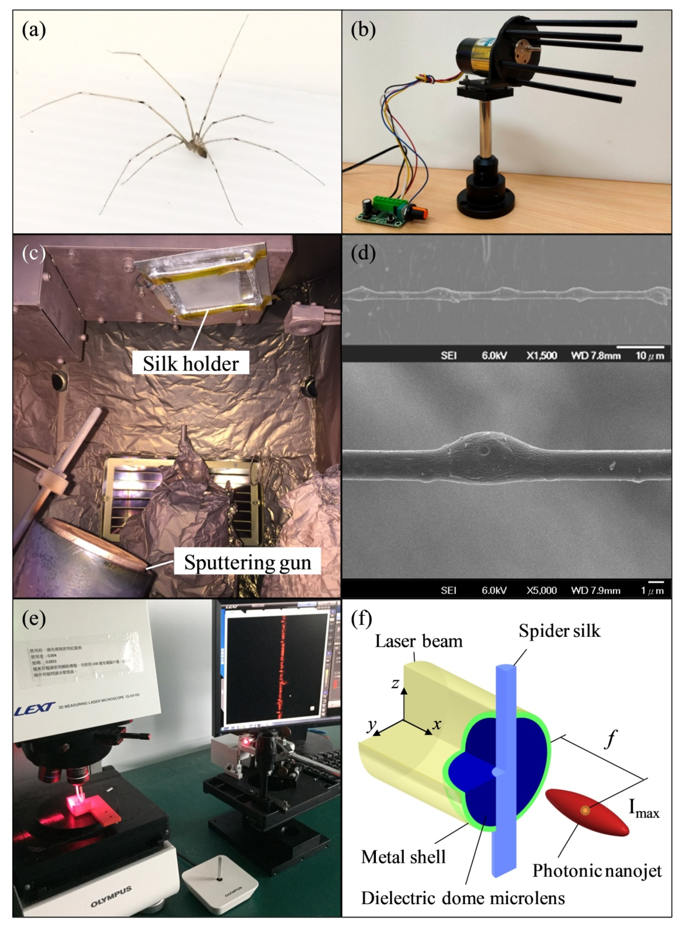
2. Experimental Methods

2.1. Metal–Dielectric Dome Microlens

The cellar spider (Pholcus phalangioides), commonly known as the “daddy long-legs”, can be found throughout the world, especially in undisturbed low-light locations. People often associate this spider with living in the corners of a rooms near the floor and ceiling. Figure 1a shows a daddy long-legs spider that usually spins its webs large, loose, and flat. A daddy long-legs spider was employed to output a single strand of silk fiber from the major ampullate gland for the experiments. Figure 1b shows the electric reeling system for silk fiber collection under controlled conditions of reeling speed, humidity, and temperature. A silk fiber with a smooth surface, circular cross-section, and uniform material quality was extracted with the reeling process. This silk fiber was a transparent medium, and the refractive index was about 1.55 in visible light region [35]. Due to the high refractive index contrast between silk fiber and the surrounding air, optical multimode guidance can be excited in the silk fiber [37]. After the reeling collection, a silk fiber with a 7 cm length and a 2 μm diameter was fixed at both ends of a specialized holder. A paraffin wax was placed below the bare silk fiber, and the photocurable resin (Everwide FP098) was dropped onto the silk’s surface. The refractive indices of the photocurable resin were 1.519, 1.503, and 1.495 for 405 nm, 532 nm, and 671 nm wavelengths, respectively. Due to the obstruction of the paraffin wax, the photocurable resin was concentrated only in one direction and formed a dome shape on the silk fiber. In the initial phase, slight resin drops condensed on the transparent puffs. As resin condensation continued, the puffs enlarged into bumps and finally became periodic dome shapes. The standing time of the photocurable resin determined the dome dimension because the silk fiber had the excellent ability of directional liquid collection. This structural wet-rebuilding ability of silk fiber has been reported in previous scientific literature [33]. Finally, the solidified dielectric dome microlens was obtained by using an ultraviolet oven (OPAS TX-500ST, Ganbow Technology Co., New Taipei City, Taiwan) and curing statically for 12 s. Furthermore, the glancing angle deposition technique was performed to coat different metal nanolayers on the dome surface [41]. Figure 1c shows the sputtering manufacturing process for coating the spider-silk-based metal-dielectric dome microlens. The metal nanolayer could be uniformly deposited on the dome surface because the silk fiber was inclined with respect to the metal target during the sputtering process. A scanning electron microscope (SEM) was employed to obtain the actual images of the dome microlens on the silk fiber. Figure 1d exhibits an SEM image of the spider-silk-based metal-dielectric dome microlens. It was observed that the diameter of the silk fiber was about 2 μm, and the uniformity of dome shape was excellent. In order to verify the metal layer’s thickness, the metal–dielectric dome microlens was cleaved by a commercial focused ion beam system (Helios NanoLab 600i, FEI, Hillscoro, OR, USA). It was clarified that the thickness of the metal nano-layer was about 5 nm. The silk-based metal–dielectric dome microlens could be utilized as a plasmonic device.

2.2. Measurement Setup

In the experiments, a commercial laser scanning digital microscope system (LEXT OLS4100, Olympus, Tokyo, Japan) was employed for measuring the optical field intensity of different metal–dielectric dome microlenses [42]. Figure 1e shows the experimental configuration of the measurement system. A diode-pumped solid-state laser with wavelengths of 405 nm, 532 nm, and 671 nm was used for illuminating the dome microlens. The metal-dielectric dome microlens was clamped on a specialized holder and fastened on a three-axis motorized stage for aligning the laser beam. The auto-focus processing, based on Olympus software, was used to obtain accurate cross-section images with a 10 nm height resolution and 120 nm lateral resolution. The experimental images of the field intensity distributions generated by the dome microlens were acquired by using an objective lens (MPLAPON100XLEXT, Olympus, Tokyo, Japan) with a working distance of 0.35 mm, a numerical aperture of 0.95, and a photomultiplier. The technical details of the commercial laser scanning digital microscope can be found on the official website for Olympus. Figure 1f shows the schematic diagram of the metal-dielectric dome microlens for photonic nanojet modulation. The convex side of the metal-dielectric dome microlens was illuminated by the laser beam along the x axis. The photonic nanojet is shown on the right side of the dome microlens. The focal length f is the axial distance from the flat side of the dome microlens to the maximum peak amplitude (Imax) along the x axis. The decay length is the axial distance from the Imax at which the intensity distribution drops to Imax/e along the x axis. The full width at half-maximum (FWHM) is the transverse width between the Imax and half-maximum point along the z axis. The finite-difference time-domain (FDTD) method was utilized to build the simulation model of the metal-dielectric dome microlens [43]. The mesh grid in the metal layer region was 1 nm for high accuracy, but the mesh grid in the dielectric and surrounding media was 20 nm for high calculation speed. Perfectly matched boundary layers were implemented along the boundaries of the simulation area. The gold-, silver-, and copper-coating layers had a refractive index of 0.54 + 2.23i, 0.05 + 3.43i, and 1.12 + 2.59i, respectively, at a wavelength of 532 nm [44]. The surrounding medium was air with a refractive index of 1.

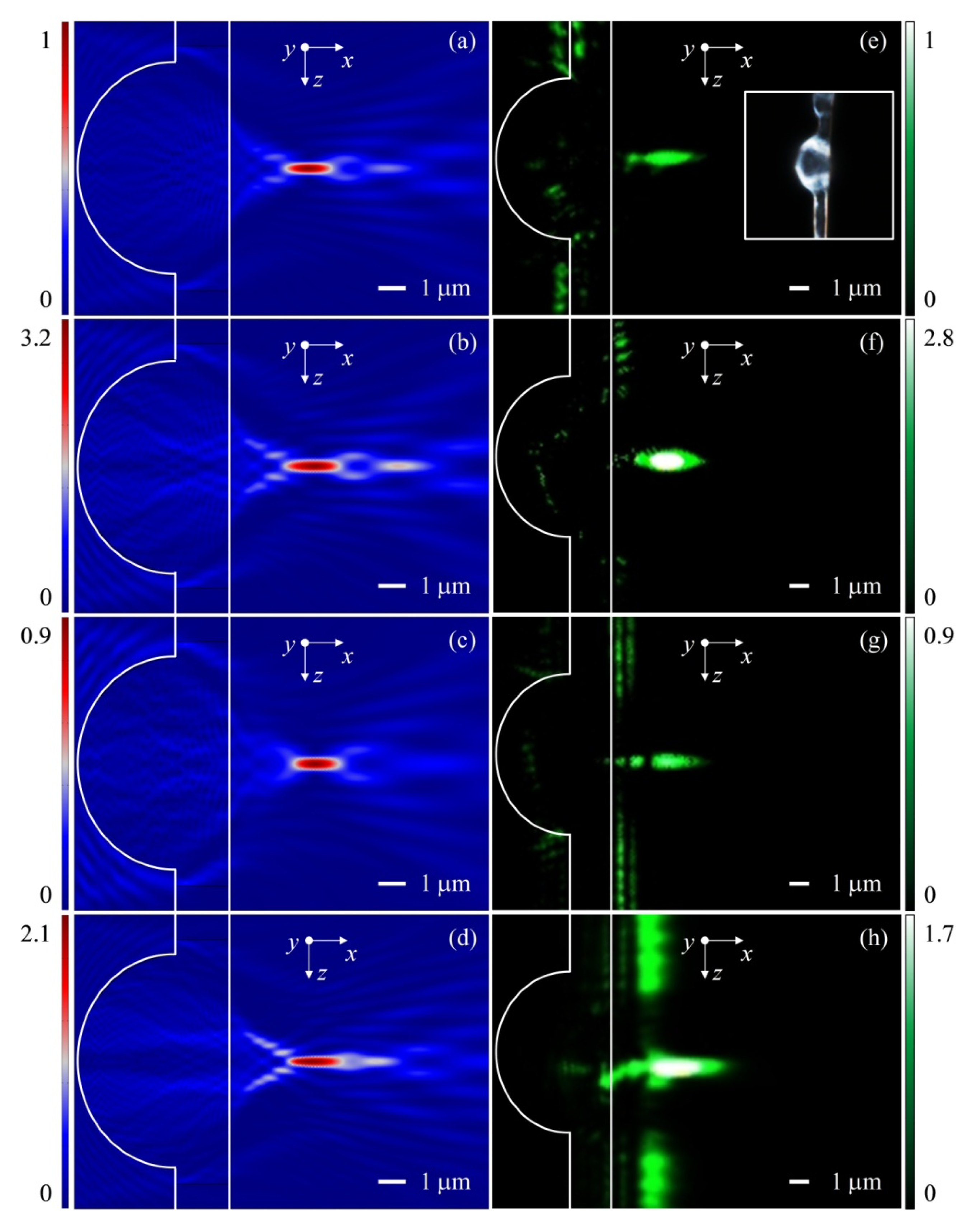
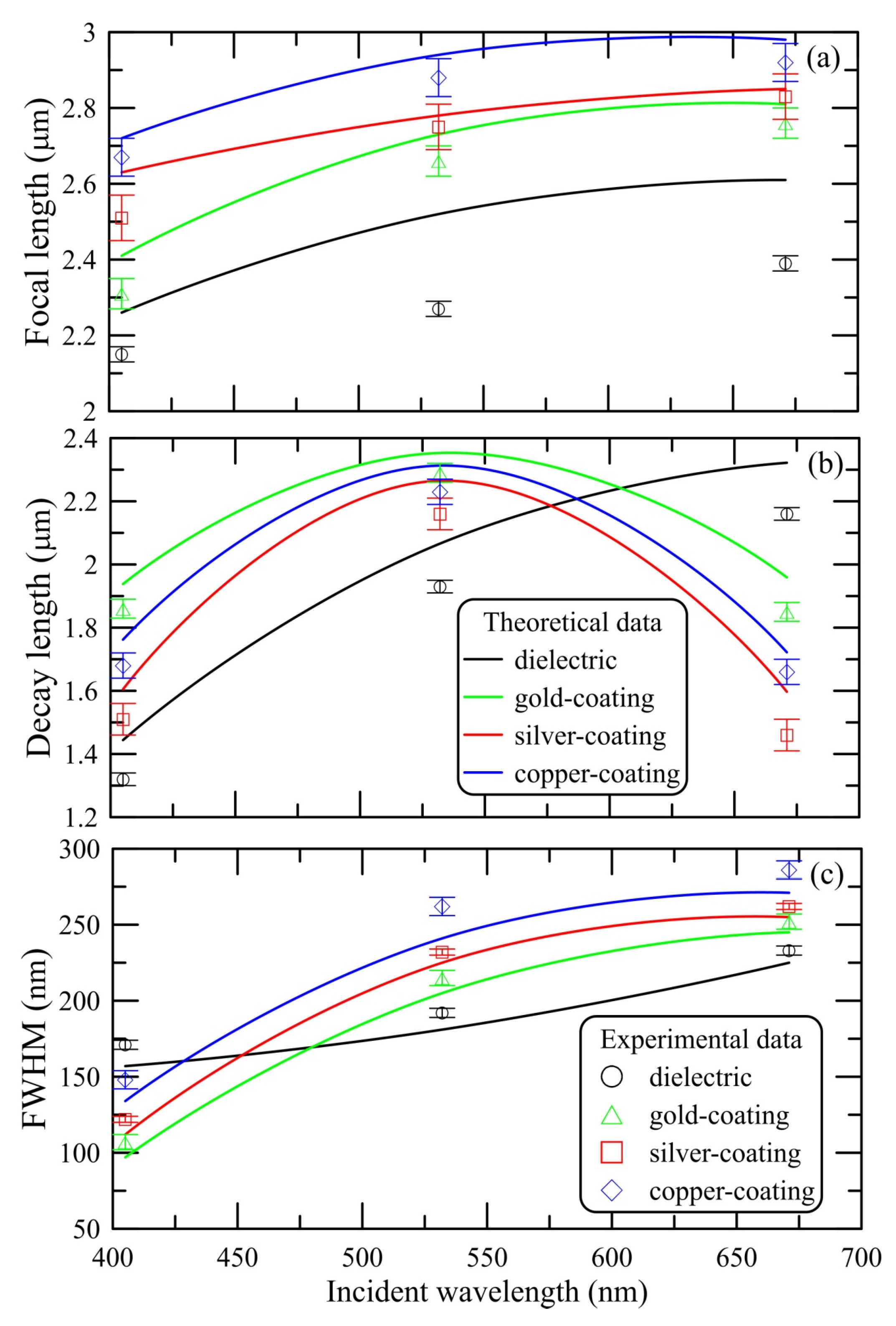
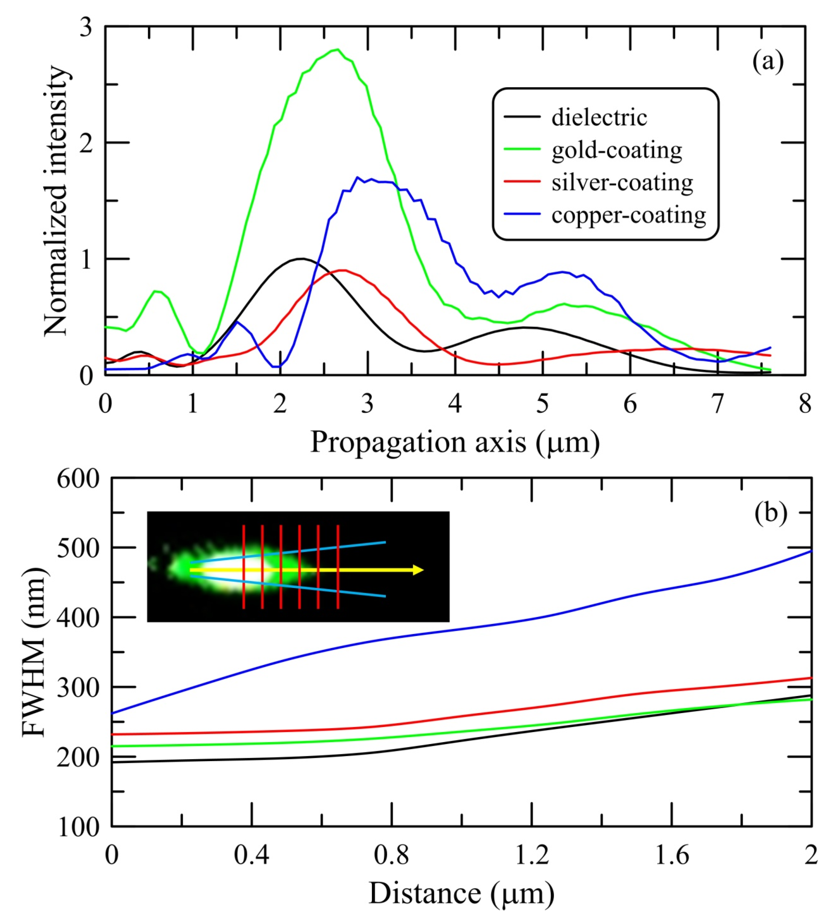
3. Results and Discussions

In order to achieve the function of photonic nanojet beam steering, it is important to be able to arbitrarily modulate the focusing property from different metal–dielectric dome microlenses. The numerical and experimental results of the photonic nanojet modulation were verified as indicated below. Figure 2a–d display the numerical results of normalized power flow patterns for the dielectric, gold-coated, silver-coated, and copper-coated dome microlenses. From the amplitude distributions, one can observe that the photonic nanojet was formed close to the surface of the microlens for the dielectric dome microlens, while it moved away from the microlens surface for the metal-coated dome microlenses. In the case of a general sphere, the photonic nanojet only has a short focal length due to the rapid convergence and divergence near the focusing point [11]. The photonic nanojet can be modified by changing the design of the engineered spheres, which leads to a sharp spot size [12]. This concept demonstrated that the dome microlens acted like a ball lens, and the focusing spot was deformed along the propagation direction by the different metal nanolayer coatings. It was also observed that the effect of the metal nanolayers on the photonic nanojet beam shaping was clarified by the power flow patterns. The maximum intensity of the photonic nanojet changed as the metal nanolayers of dome microlenses changed. As seen from the power flow patterns, the intensity of the photonic nanojet was effectively amplified by coating a gold nanolayer on the dome surface, due to the surface plasmon polaritons [45].
Figure 2e–h display the direct experimental images of the intensity distribution for different metal-dielectric dome microlenses at a 532 nm wavelength for verification. Compared with the simulation results, the focusing effect of the photonic nanojet is exhibited clearly in the raw images. Apparently, the field intensity distributions of the experiments were largely in agreement with the simulation results. As shown in Figure 2a,e, the dielectric dome microlens generated the photonic nanojet, the shape of which behaved in a manner similar to a stiletto knife. The field intensity distributions around the focusing point were nearly parallel, and therefore formed a narrow strip. It can be seen in Figure 2f that the focusing intensity of the gold-coated dome microlens was enhanced significantly due to the surface plasmon resonance. The photonic nanojet’s focus with the surface plasmon resonance was almost three times the field intensity of the dielectric dome microlens. Controllable photonic nanojet formation excited by plasmonic effects can be described by the dispersion relation of the surface plasmon polaritons [45,46]. The experimental image in Figure 2g demonstrates that the surface plasmon absorption excited on the silver layer caused the intensity reduction of the photonic nanojet for the silver-coated dome microlens. In Figure 2h, the dispersion effect on the surface of the copper-coated dome microlens can be observed due to the surface plasmon scattering. The surface-dependent reflectance arose from the copper layer, and the optical beam was dispersed from the layer surface.
To quantitatively estimate the quality of the photonic nanojet, we determined several critical parameters from the field intensity distribution. Figure 3 shows the critical parameters as a function of the incident wavelength for the dome microlenses with different metal coatings. The focal lengths at a 532 nm wavelength were measured to be 2.27 μm, 2.66 μm, 2.75 μm, and 2.88 μm for the dielectric, gold-coated, silver-coated, and copper-coated dome microlenses, respectively. The focal length increased as the incident wavelength increased. Compared to the dielectric dome microlens, the focal length was increased by 27% for the copper-coated dome microlens. The focal length could be adjusted by varying the metal layer. When the dome microlens was coated with a metal layer, the focal length was large enough to meet the working distance for microlens-aided imaging [2]. In Figure 3b, the decay lengths at a 532 nm wavelength were measured to be 1.93 μm, 2.29 μm, 2.16 μm, and 2.23 μm for the dielectric, gold-coated, silver-coated, and copper-coated dome microlenses, respectively. It was observed that the decay length had a maximum value at an incident wavelength of 532 nm for all the metal-dielectric dome microlenses. In Figure 3c, the transverse FWHMs at a 532 nm wavelength were measured to be 192 nm, 215 nm, 232 nm, and 263 nm for the dielectric, gold-coated, silver-coated, and copper-coated dome microlenses, respectively. The transverse FWHM of the photonic nanojet decreased as the incident wavelength decreased. As the incident wavelength decreased to 405 nm, the corresponding FWHM became significantly less than 0.5λ via the experimental verifications. The suggested metal-dielectric dome microlenses showed great potential for far-field super-resolution lithography and imaging applications [42].
Figure 4a shows the normalized intensity distributions of photonic nanojets for the different metal-dielectric dome microlenses along the propagation axis (x axis). The origin of the longitudinal profile along the propagation axis was located at the flat surface of the dome microlenses. All intensity profiles were normalized to the intensity profile for the dielectric dome microlens. The photonic nanojet generated by dome microlenses emerged in the form of a Gaussian distribution with an exponentially decaying trail. The length of the photonic nanojet increased as the dome microlens was coated with metal layer, and the field intensity was enhanced as well. The maximum intensity increased by 180% for the gold coating, although the maximum intensity decreased by 10% for the silver coating. Depending on the metal layer, we observed that not only the intensity of the photonic nanojet was enhanced, but the effective length of the photonic nanojet also was elongated. The engineered metal–dielectric dome microlens is expected to provide high concentration and low divergence in the focusing point [24].
Figure 4b shows the FWHM as a function of the propagation distance for the photonic nanojets with different metal–dielectric dome microlenses. The origin of the propagation distance corresponded to the point of maximal peak amplitude. The slope of the straight fitting line was used to determine the divergence angle of the photonic nanojets [7]. The divergence angles at a 532 nm wavelength were measured to be 6.3°, 2.6°, 3.8°, and 7.2° for the dielectric, gold-coated, silver-coated, and copper-coated dome microlenses, respectively. The proposed metal-coated dome microlens can work with a low divergence angle and long focal length, which is not possible for dielectric spherical microlenses. It was apparent that the divergence angle of the designed dome microlens was sensitive to the refractive index of the surrounding medium. When the dome microlens was coated with a metal layer, the refractive index of the surrounding medium could be found indirectly by measuring the divergence angle. Both the above-mentioned experimental and simulation results confirmed that the metal-dielectric dome microlens with flexible photonic nanojet modulation was suitable for a plasmonic sensor of the refractive index [47].

4. Conclusions

In this work, photonic nanojet modulation based on a metal-dielectric dome microlens was first theoretically and experimentally demonstrated with an extended focal length, narrow beam waist, long effective length, and low divergence angle. The directional liquid collection capability of wet-rebuilt silk fiber was utilized for the formation of the dielectric dome microlens. The dielectric dome microlens was coated with different metal layers by using the glancing angle deposition technique. Through FDTD simulation and experimental analysis, we concluded that the improvement of the photonic nanojet was attributed to the nature of surface plasmon polaritons, which caused a high concentration near the metal-dielectric interface. The gold-coated dome microlens had an intensity enhancement of about three times due to surface plasmon resonance. The focal length of the photonic nanojet was increased by 27% for the copper-coated dome microlens. A minimum divergence angle of 2.6° was achieved by the gold-coated dome microlens. Moreover, the proposed metal-dielectric dome microlens showed compatibility with the adjacent wavelengths and a spot width less than half-wavelength. These kinds of plasmonic microlenses have great potential in far-field flexible parallel lithography with a sub-wavelength line width.

Author Contributions

Conceptualization, C.-B.L. and C.-Y.L.; methodology, C.-B.L. and C.-Y.L.; software, C.-Y.L. and W.-Y.C.; validation, C.-Y.L. and W.-Y.C.; formal analysis, C.-B.L. and Y.-H.L.; resources, C.-Y.L.; data curation, Y.-H.L. and W.-Y.C.; writing—original draft preparation, C.-Y.L.; writing—review and editing, C.-B.L. and C.-Y.L.; visualization, C.-Y.L. and W.-Y.C.; supervision, C.-B.L. and C.-Y.L.; project administration, C.-Y.L. and W.-Y.C.; funding acquisition, C.-Y.L. All authors have read and agreed to the published version of the manuscript.

Funding

This research was funded by the Ministry of Science and Technology of Taiwan (MOST 108-2221-E-010-012-MY3, MOST 109-2923-E-010-001-MY2) and the Yen Tjing Ling Medical Foundation (CI-110-28).

Institutional Review Board Statement

Not applicable.

Informed Consent Statement

Not applicable.

Data Availability Statement

The data that support the findings of this study are available from the corresponding author upon reasonable request.

Conflicts of Interest

The authors declare no conflict of interest.

References

  1. Allen, K.; Farahi, N.; Li, Y.; Limberopoulos, N.; Walker, D., Jr.; Urbas, A.; Liberman, V.; Astratov, V. Super-resolution mi-croscopy by movable thin-films with embedded microspheres: Resolution analysis. Ann. Phys. 2015, 527, 513–522. [Google Scholar] [CrossRef] [Green Version]
  2. Chen, L.; Zhou, Y.; Li, Y.; Hong, M. Microsphere enhanced optical imaging and patterning: From physics to applications. Appl. Phys. Rev. 2019, 6, 021304. [Google Scholar] [CrossRef]
  3. Chen, Z.; Taflove, A.; Backman, V. Photonic nanojet enhancement of backscattering of light by nanoparticles: A potential novel visible-light ultramicroscopy technique. Opt. Express 2004, 12, 1214–1220. [Google Scholar] [CrossRef] [PubMed]
  4. Li, X.; Chen, Z.; Taflove, A.; Backman, V. Optical analysis of nanoparticles via enhanced backscattering facilitated by 3-D photonic nanojets. Opt. Express 2005, 13, 526–533. [Google Scholar] [CrossRef] [PubMed] [Green Version]
  5. Ferrand, P.; Wenger, J.; Devilez, A.; Pianta, M.; Stout, B.; Bonod, N.; Popov, E.; Rigneault, H. Direct imaging of photonic nanojets. Opt. Express 2008, 16, 6930–6940. [Google Scholar] [CrossRef] [PubMed]
  6. Kim, M.; Scharf, T.; Mühlig, S.; Rockstuhl, C.; Herzig, H.P. Engineering photonic nanojets. Opt. Express 2011, 19, 10206–10220. [Google Scholar] [CrossRef]
  7. McCloskey, D.; Wang, J.; Donegan, J. Low divergence photonic nanojets from Si3N4 microdisks. Opt. Express 2012, 20, 128–140. [Google Scholar] [CrossRef]
  8. Han, L.; Han, Y.; Wang, J.; Cui, Z. Internal and near-surface electromagnetic fields for a dielectric spheroid illuminated by a zero-order Bessel beam. J. Opt. Soc. Am. A 2014, 31, 1946–1955. [Google Scholar] [CrossRef]
  9. Liu, C.; Chen, C. Characterization of photonic nanojets in dielectric microdisks. Phys. E Low Dimens. Syst. Nanostruct. 2015, 73, 226–234. [Google Scholar] [CrossRef]
  10. Liu, C.; Lin, F. Geometric effect on photonic nanojet generated by dielectric microcylinders with non-cylindrical cross-sections. Opt. Commun. 2016, 380, 287–296. [Google Scholar] [CrossRef]
  11. Wu, M.; Chen, R.; Ling, J.; Chen, Z.; Chen, X.; Ji, R.; Hong, M. Creation of a longitudinally polarized photonic nanojet via an engineered microsphere. Opt. Lett. 2017, 42, 1444–1447. [Google Scholar] [CrossRef] [PubMed]
  12. Zhou, Y.; Gao, H.; Teng, J.; Luo, X.; Hong, M. Orbital angular momentum generation via a spiral phase microsphere. Opt. Lett. 2018, 43, 34–37. [Google Scholar] [CrossRef]
  13. Liu, C.; Yeh, M. Experimental verification of twin photonic nanojets from a dielectric microcylinder. Opt. Lett. 2019, 44, 3262–3265. [Google Scholar] [CrossRef] [PubMed]
  14. Minin, I.; Liu, C.; Geints, Y.; Minin, O. Recent advantages in integrated photonic jet-based photonics. Photonics 2020, 7, 41. [Google Scholar] [CrossRef]
  15. Heifetz, A.; Kong, S.; Sahakian, A.; Taflove, A.; Backman, V. Photonic nanojets. J. Comput. Theor. Nanosci. 2009, 6, 1979–1992. [Google Scholar] [CrossRef]
  16. Luk’Yanchuk, B.; Paniagua-Dominguez, R.; Minin, I.V.; Minin, O.V.; Wang, Z. Refractive index less than two: Photonic nanojets yesterday, today and tomorrow. Opt. Mater. Express 2017, 7, 1820–1847. [Google Scholar] [CrossRef]
  17. Wang, Z.; Guo, W.; Luk’yanchuk, B.; Whitehead, D.; Li, L.; Liu, Z. Optical near-field interaction between neighbouring mi-cro/nano-particles. J. Laser Micro Nanoeng. 2008, 3, 14–18. [Google Scholar] [CrossRef] [Green Version]
  18. Rizzato, S.; Primiceri, E.; Monteduro, A.; Colombelli, A.; Leo, A.; Manera, M.; Rella, R.; Maruccio, G. Interaction-tailored or-ganization of large-area colloidal assembliesr. Beilstein J. Nanotechnol. 2018, 9, 1582–1593. [Google Scholar] [CrossRef] [Green Version]
  19. Geints, Y.; Panina, E.; Zemlyanov, A. Collective effects in the formation of an ensemble of photonic nanojets by an ordered microassembly of dielectric microparticles. Atmos. Ocean. Opt. 2019, 32, 113–119. [Google Scholar] [CrossRef]
  20. Geints, Y.; Zemlyanov, A.; Panina, E. Peculiarities of the formation of an ensemble of photonic nanojets by a micro-assembly of conical particles. Quantum Electron. 2019, 49, 210–215. [Google Scholar] [CrossRef]
  21. Geints, Y.; Zemlyanov, A.; Panina, E. Photonic nanojet calculations in layered radially inhomogeneous micrometer-sized spherical particles. J. Opt. Soc. Am. B 2011, 28, 1825–1830. [Google Scholar] [CrossRef]
  22. Shen, Y.; Wang, L.; Shen, J. Ultralong photonic nanojet formed by a two-layer dielectric microsphere. Opt. Lett. 2014, 39, 4120–4123. [Google Scholar] [CrossRef] [PubMed] [Green Version]
  23. Pacheco-Peña, V.; Beruete, M.; Minin, I. Terajets produced by dielectric cuboids. Appl. Phys. Lett. 2014, 105, 084102. [Google Scholar] [CrossRef] [Green Version]
  24. Liu, C.; Hsiao, K. Direct imaging of optimal photonic nanojets from core-shell microcylinders. Opt. Lett. 2015, 40, 5303–5306. [Google Scholar] [CrossRef]
  25. Geints, Y.; Zemlyanov, A.; Panina, E. Microaxicon-generated photonic nanojets. J. Opt. Soc. Am. B 2015, 32, 1570–1574. [Google Scholar] [CrossRef]
  26. Minin, I.V.; Minin, O.V.; Geints, Y. Localized EM and photonic jets from non-spherical and non-symmetrical dielectric mesoscale objects: Brief review. Ann. Phys. 2015, 527, 491–497. [Google Scholar] [CrossRef] [Green Version]
  27. Degtyarev, S.; Porfirev, A.; Khonina, S. Photonic nanohelix generated by a binary spiral axicon. Appl. Opt. 2016, 55, B44–B48. [Google Scholar] [CrossRef] [PubMed]
  28. Geints, Y.; Minin, I.V.; Panina, E.; Zemlyanov, A.; Minin, O.V. Comparison of photonic nanojets key parameters produced by nonspherical microparticles. Opt. Quantum Electron. 2017, 49, 118. [Google Scholar] [CrossRef]
  29. Mahariq, I.; Giden, I.; Kurt, H.; Minin, O.V.; Minin, I.V. Strong electromagnetic field localization near the surface of hemicy-lindrical particles. Opt. Quant. Electron. 2018, 50, 423. [Google Scholar] [CrossRef]
  30. Zhang, B.; Hao, J.; Shen, Z.; Wu, H.; Zhu, K.; Xu, J.; Ding, J. Ultralong photonic nanojet formed by dielectric microtoroid structure. Appl. Opt. 2018, 57, 8331–8337. [Google Scholar] [CrossRef]
  31. Liu, X.; Zhou, H.; Yang, M.; Xie, Z.; Han, Q.; Gou, J.; Wang, J. Photonic nanojets with ultralong working distance and narrowed beam waist by immersed engineered dielectric hemisphere. Opt. Express 2020, 28, 33959–33970. [Google Scholar] [CrossRef]
  32. Omenetto, F.; Kaplan, D. A new route for silk. Nat. Photonics 2008, 2, 641–643. [Google Scholar] [CrossRef]
  33. Zheng, Y.; Bai, H.; Huang, Z.; Tian, X.; Nie, F.; Zhao, Y.; Zhai, J.; Jiang, L. Directional water collection on wetted spider silk. Nat. Cell Biol. 2010, 463, 640–643. [Google Scholar] [CrossRef]
  34. Rising, A.; Johansson, J. Toward spinning artificial spider silk. Nat. Chem. Biol. 2015, 11, 309–315. [Google Scholar] [CrossRef]
  35. Little, D.; Kane, D. Image contrast immersion method for measuring refractive index applied to spider silks. Opt. Express 2011, 19, 19182–19189. [Google Scholar] [CrossRef] [PubMed]
  36. Huby, N.; Vié, V.; Renault, A.; Beaufils, S.; Lefèvre, T.; Paquet-Mercier, F.; Pézolet, M.; Bêche, B. Native spider silk as a biological optical fiber. Appl. Phys. Lett. 2013, 102, 123702. [Google Scholar] [CrossRef] [Green Version]
  37. Applegate, M.; Perotto, G.; Kaplan, D.; Omenetto, F. Biocompatible silk step-index optical waveguides. Biomed. Opt. Express 2015, 6, 4221–4227. [Google Scholar] [CrossRef] [PubMed] [Green Version]
  38. Kujala, S.; Mannila, A.; Karvonen, L.; Kieu, K.; Sun, Z. Natural Silk as a Photonics Component: A Study on Its Light Guiding and Nonlinear Optical Properties. Sci. Rep. 2016, 6, 22358. [Google Scholar] [CrossRef] [PubMed] [Green Version]
  39. Monks, J.; Yan, B.; Hawkins, N.; Vollrath, F.; Wang, Z. Spider Silk: Mother Nature’s Bio-Superlens. Nano Lett. 2016, 16, 5842–5845. [Google Scholar] [CrossRef] [PubMed] [Green Version]
  40. Tow, K.; Chow, D.; Vollrath, F.; Dicaire, I.; Gheysens, T.; Thevenaz, L. Exploring the Use of Native Spider Silk as an Optical Fiber for Chemical Sensing. J. Light. Technol. 2017, 36, 1138–1144. [Google Scholar] [CrossRef] [Green Version]
  41. Wakefield, N.; Sorge, J.; Taschuk, M.; Bezuidenhout, L.; Brett, M.; Sit, J. Control of the principal refractive indices in biaxial metal oxide films. J. Opt. Soc. Am. A 2011, 28, 1830–1840. [Google Scholar] [CrossRef]
  42. Zhu, H.; Yan, B.; Zhou, S.; Wang, Z.; Wu, L. Synthesis and super-resolution imaging performance of a refrac-tive-index-controllable microsphere superlens. J. Mater. Chem. C 2015, 3, 10907–10915. [Google Scholar] [CrossRef] [Green Version]
  43. Taflove, A.; Hagness, S. Computational Electrodynamics: The Finite Difference Time Domain Method; Artech House: Norwood, MA, USA, 2005. [Google Scholar]
  44. Johnson, P.; Christy, R. Optical Constants of the Noble Metals. Phys. Rev. B 1972, 6, 4370–4379. [Google Scholar] [CrossRef]
  45. Ju, D.; Pei, H.; Jiang, Y.; Sun, X. Controllable and enhanced nanojet effects excited by surface plasmon polariton. Appl. Phys. Lett. 2013, 102, 171109. [Google Scholar] [CrossRef]
  46. Minin, I.V.; Minin, O.V.; Glinskiy, I.; Khabibullin, R.; Malureanu, R.; Lavrinenko, A.; Yakubovsky, D.; Arsenin, A.; Volkov, V.; Ponomarev, D. Plasmonic nanojet: An experimental demonstration. Opt. Lett. 2020, 45, 3244–3247. [Google Scholar] [CrossRef]
  47. Liu, X.; Wang, J.; Gou, J.; Ji, C.; Cui, G. Optical Properties and Sensing Performance of Au/SiO2 Triangles Arrays on Reflection Au Layer. Nanoscale Res. Lett. 2018, 13, 335. [Google Scholar] [CrossRef]
Figure 1. (a) A photo of a daddy long-legs spider. (b) The electric reeling system for the spider silk. (c) The sputtering manufacturing process for coating the spider-silk-based metal–dielectric dome microlens. (d) An SEM image of the dome microlens. (e) The laser scanning digital microscope system for measuring the dome microlens. (f) A schematic diagram of the dome microlens for photonic nanojet modulation.
Photonics 08 00334 g001
Figure 2. Numerical results of normalized power flow patterns for the (a) dielectric, (b) gold-coated, (c) silver-coated, and (d) copper-coated dome microlenses; and raw experimental images of the (e) dielectric, (f) gold-coated, (g) silver-coated, and (h) copper-coated dome microlenses. The incident wavelength was 532 nm for all the dome microlenses. The inset is a microphotograph of the spider-silk-based dome microlens.
Photonics 08 00334 g002
Figure 3. Critical parameters as a function of incident wavelength for the dome microlenses with different metal coatings: (a) focal length, (b) decay length, and (c) FWHM.
Photonics 08 00334 g003
Figure 4. (a) Normalized intensity distributions of photonic nanojets for different metal-dielectric dome microlenses along the propagation axis (x axis). (b) FWHM as a function of the propagation distance for photonic nanojets for the different metal-dielectric dome microlenses. The inset indicates that the yellow arrow is the propagation direction, the red lines are the positions of serial cross-sections for the FWHM, and the blue lines are the straight fitting lines.
Photonics 08 00334 g004
Publisher’s Note: MDPI stays neutral with regard to jurisdictional claims in published maps and institutional affiliations.

