Review

A Review of Transparent Sensors for Photoacoustic Imaging Applications

1
Research Center for Intelligent Sensing, Zhejiang Lab, Hangzhou 311121, China
2
Department of Biomedical Engineering, University of Southern California, Los Angeles, CA 90089, USA
*
Author to whom correspondence should be addressed.
These authors contributed equally to this work.
Photonics 2021, 8(8), 324; https://doi.org/10.3390/photonics8080324
Submission received: 2 July 2021 / Revised: 23 July 2021 / Accepted: 27 July 2021 / Published: 10 August 2021
(This article belongs to the Special Issue Photoacoustic Imaging and Systems)

Abstract

:
Photoacoustic imaging is a new type of noninvasive, nonradiation imaging modality that combines the deep penetration of ultrasonic imaging and high specificity of optical imaging. Photoacoustic imaging systems employing conventional ultrasonic sensors impose certain constraints such as obstructions in the optical path, bulky sensor size, complex system configurations, difficult optical and acoustic alignment, and degradation of signal-to-noise ratio. To overcome these drawbacks, an ultrasonic sensor in the optically transparent form has been introduced, as it enables direct delivery of excitation light through the sensors. In recent years, various types of optically transparent ultrasonic sensors have been developed for photoacoustic imaging applications, including optics-based ultrasonic sensors, piezoelectric-based ultrasonic sensors, and microelectromechanical system-based capacitive micromachined ultrasonic transducers. In this paper, the authors review representative transparent sensors for photoacoustic imaging applications. In addition, the potential challenges and future directions of the development of transparent sensors are discussed.

1. Introduction

Photoacoustic imaging (PAI), based on the photoacoustic (PA) effect, is a new type of noninvasive, nonradiation biomedical imaging modality that has been rapidly developing in recent years [1,2], as it combines the deep penetration of ultrasonic (US) imaging and the high specificity of optical imaging. PAI can acquire structural and functional information from most soft tissues, and provides highly specific tissue and molecular images [3,4,5,6,7,8]. In PAI, the biological tissue is irradiated by a pulsed laser within a safe range. A portion of the optical energy is absorbed by the tissue and converted into heat, resulting in a transient temperature rise. Periodic temperature changes cause a thermoelastic effect, which excites high-frequency acoustic waves. A US sensor, also called a US transducer, is often used to detect the excited high-frequency and wide-band PA signals from the target tissue irradiated by the laser pulses, which makes it possible to combine rich optical contrast and deep acoustic penetration beyond the optical diffraction limit [8,9,10,11,12]. To collect PA signals without too much attenuation, the US sensor should be positioned near the target tissue [13,14]. Nevertheless, conventional optically opaque US sensors make the effective delivery of the laser difficult, and can even completely block out light. To allow the laser to pass through the US sensor directly to the surface of the tissues without much loss, doughnut-shaped or hollow-shaped US sensors have been developed in PAI [13,15,16]. However, the acoustic sensitivity and focusing ability of the US sensor will be reduced due to the removal of its central part, and this type of US sensor is too big to obtain a better spatial resolution comparable with optical microscopy.
To overcome these drawbacks, a US sensor in the optically transparent form has been introduced, as it enables direct delivery of excitation light through the sensors. In recent years, various types of optically transparent US sensors have been developed for PAI applications. These sensors can be divided into three main categories: optics-based US sensors, piezoelectric-based US sensors, and microelectromechanical system (MEMS)-based capacitive micromachined ultrasonic transducers (CMUTs). Optics-based US sensors mainly include Fabry-Perot (FP) etalons (FP) [17,18], micro-ring resonators (MRRs) [19,20,21,22], and grating-based sensors [23,24,25]. Transparent piezoelectric-based US sensors use piezoelectric materials that have sufficient optical transmittance, such as polyvinylidene fluoride (PVDF) polymer films [26,27] and lithium niobite (LN) single crystals [28,29,30,31,32]. Transparent CMUT is a new type of optically transparent US sensors, which has a limited operating frequency (less than 20 MHz) and is expensive due to the specialized MEMS fabrication techniques [33,34,35].
In this paper, we aim to review recent advances in transparent sensors for PAI applications, focusing on various types of transparent US sensors, as well as their corresponding materials and techniques. In addition, potential challenges and future directions in the development of transparent sensors are discussed.

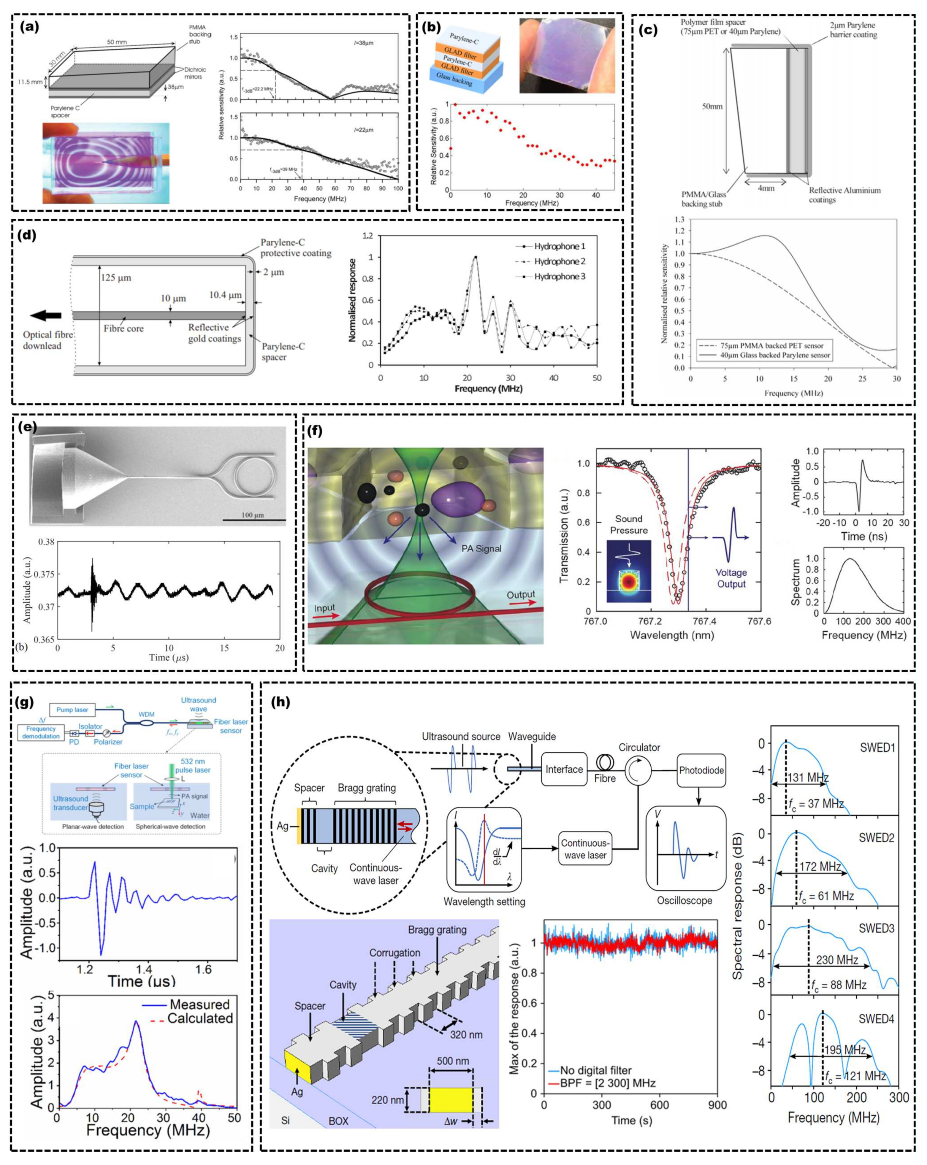
2. Transparent Optics-Based US Sensors

The use of optical interference or resonance methods to detect PA signals without contact has become a hotspot in research on PAI technology in recent years [36,37,38]. It is also an effective method to achieve noncontact PA detection and imaging without using acoustic coupling media. In an optical US detection system, the physical properties of ultrasound (pressure, displacement) are converted into physical properties of optics (wavelength, optical path length) through optical interference or resonance, and then all properties are displayed by voltages. The noncontact and nondestructive characteristics of most types of optical US detection technology give it broad application prospects in nondestructive testing and evaluation, and it can perform real-time detection of an object under test in an environment of radiation, high temperature, and high pressure [8,11]. At the current stage, common types of optically transparent US sensors are FP interferometer sensors, MRRs, and grating-based sensors [22,23,24,25,39,40,41,42,43,44]. Optical detection methods have the following advantages over conventional US detection methods:
  • With the good directionality of the laser, FP sensors can achieve long-distance measurement [41,45,46];
  • Most FP sensors and MRR sensors are noncontact and so can avoid the error and pollution caused by the contact between the couplant and the workpiece during traditional US detection, therefore realizing truly nondestructive testing [37,41,42,47];
  • The sensitivity is independent of the detector size, and the bandwidth is much wider; the transparent nature of the optical detectors simplifies the light delivery in the system [36,37].
An FP interferometer is made of a thin diaphragm and the optical fiber end-face as two reflectors. The key component of this technology is the use of an especially made FP interferometer film, which can convert the weak vibration of the PA signal into the micro displacement of the film with the cavity length changing, and then can be demodulated by optical interference. The technology can penetrate to a depth of several millimeters with a lateral resolution of tens to hundreds of microns [46,48,49]. FP sensors have plenty of advantages including not being subject to electromagnetic interference, a high-frequency response, small size, etc. In recent years, various kinds of materials can be used as the mirrors in the FP cavity, such as silica, silver, and graphene. The sensitivity of the sensor can be improved using a smaller thickness and larger diameter of diaphragm [40,41,42,45,46,48,49,50]. In some studies, the introduction of MEMS technology can produce diaphragms with a smaller thickness and a smaller diameter to achieve a higher detection frequency. Ashjenazi et al. used vacuum evaporation of a thin gold layer as the first mirror, then spin-coating of a polymer layer (SU-8 photoresist) to form the diaphragm, then another gold evaporation as the second mirror. The total thickness of the FP sensor is 10 μm. The FP sensor is manufactured on a glass substrate, which has a detection signal:noise ratio (SNR) better than piezoelectric-based sensors over 100 MHz bandwidth. The noise equivalent pressure (NEP) of the FP sensor is 0.2 Pa / Hz over a 50 MHz band [40]. This proves that the FP sensor is a promising alternative to piezoelectric detection in high-resolution PAI applications. Pham et al. fabricated a FP sensor, which consists of two highly reflecting dichroic mirrors separated by a 20 μm thick spacer made of Parylene C. Most of the range of frequency attenuation in the transmission process in the carbon nanotube polydimethylsiloxane (CNT-PDMS) film is relatively weak; for example, a 100 μm film attenuates frequencies up to 22 MHz by less than 1.7 dB [39]. The FP sensor also uses the CNT-PDMS composite film as the US transmitting layer for pulse-echo imaging [41]. The −6 dB bandwidth of the FP sensor is 22 MHz, which is a much wider bandwidth than for conventional piezoelectric-based US detectors. In addition, the sensor has higher resolution for tissue imaging and better image quality than conventional piezoelectric-based US scanners. It can achieve high resolution in tissue up to depth of 10 mm in vivo PAI [41]. Zhang et al. fabricated a FP sensor, which is composed of a 38 μm thick Parylene C film, two dichroic mirrors, and a polymethylmethacrylate (PMMA) backing stub. The wedge-shaped PMMA backing stub is used to eliminate the parasitic interference between the light reflected from its upper surface and the FP sensor. The schematic of the FP sensor is shown in Figure 1a. The −3 dB FP sensor bandwidth of the FP sensor is 22 MHz, and the measured noise equivalent pressure of the FP sensor is 210 Pa over a 20 MHz measurement bandwidth. Figure 1b–d shows other typical FP sensors, which are all made of various polymer materials. The above research proved that FP sensors with a polymer film as the spacer can provide broad-frequency responses of the order of several tens of megahertz and have high sensitivity comparable to piezoelectric-based sensors.
MRR is another sensor to detect US waves, which is composed of a close bus waveguide and a ring-shaped resonator separated by a low dielectric gap. The principle for detecting US is as follows: The US wave will cause the deformation of the ring resonator, which will cause a change in the effective optical path length and then a shift in the resonance frequency. Changes will be detected by a photodiode or a wavelength meter to deduce information about the US signals [22,37,43,44,47]. MRR has plenty of unique advantages as follows:
  • The use of sub-millimeter size MRR can achieve high-sensitivity US wave detection because the effective optical path length of the system is amplified by several orders of magnitude through strong optical resonance, which can minimize the interference to the optical path of the optical microscope system;
  • MRR provides a wider US wave detection bandwidth, therefore improving the saturation limit and axial resolution of functional PAI. The optical frequency is much higher than the US frequency, so the MRR can still provide a significantly wider detection bandwidth compared with conventional piezoelectric-based sensors;
  • The miniaturized MRR detector allows sensitive US detection within a larger detection angle, which is beneficial to increase the field of view in the laser scanning PAI system [36,37,54,55].
The design of an MRR detector is shown in Figure 1e [54] and Figure 1f [20]. Li et al. designed a miniaturized optical transparent MRR to detect US waves [22]. The MRR consists of a circular and a matching bus waveguide, which is fabricated on a fused quartz coverslip. The total thickness of the device is 250 μm. The axial resolution of the MRR is 5.3 μm. The device has a high sensitivity (~6.8 Pa) over a wide receiving angle with a bandwidth of 140 MHz. Moreover, compared to the conventional piezoelectric-based sensors, MRR can nearly double the PA saturation limit. Chao et al. chose polystyrene as the waveguide material, which gave the MRR high sensitivity due to the low Young’s modulus of the polystyrene [43]. The waveguides of the MRR are 2.4 μm wide and 1.85 μm height and are operated at an optical waveguide length of 1550 nm. The NEP is about 150 kPa with a 40 MHz bandwidth. Zhang et al. proposed an MRR sensor with unprecedented broad bandwidth response from DC to ~350 MHz at −3 dB and an ultralow noise equivalent pressure of 105 Pa in this frequency range. The axial resolution in the PAI will be improved to sub-3 μm due to the ultrabroad frequency response and the ultrahigh sensitivity. The MRR also uses polystyrene as a waveguide material, and the size is 69 μm diameter and 1.4 μm height [44]. The reports prove that the polymer MRR is a promising sensor for applications in PAI due to its ultrabroad bandwidth and high sensitivity.
The grating-based sensor is a major type of optical detection, which is mainly composed of Bragg gratings and a laser cavity [25]. When the ultrasonic wave hits the sensors, the birefringence caused by the stress will cause a frequency shift of the beat signal, which can be detected based on I/Q phase demodulation [24]. The grating-based sensors have a high sensitivity per unit area, electromagnetic interference (EMI) immunity, and wide frequency bandwidth [24,36,37]. The design of a grating-based sensor is shown in Figure 1g [23] and Figure 1h [25]. Bai et al. manufactured an optical US sensor, which is made of two highly reflective ultraviolet-inscribed Bragg gratings in a single mode fiber (12 μm in diameter) to form a laser cavity [23]. On account of the broadband frequency response and the common-mode cancellation, the sensor can resist vibration and temperature changes [23,56]. The NEP of the sensor is 45 Pa with a sampling rate of 100 MHz and the −3 dB bandwidth is 18 MHz [23]. Shnaiderman et al. designed a point-like silicon waveguide-etalon detector (SWED) by exploiting the high-throughput fabrication techniques that are used in the semiconductor industry [25]. They made a single continuous silicon waveguide divided into four sections: an Ag layer, a spacer, a cavity, and a Bragg grating. The optical sensor is small, with a sensing area of only 220 nm by 500 nm. The −6 dB bandwidth is 230 MHz. The NEP of the SWED is 45 mPa / Hz over a 25 MHz bandwidth [25]. According to the reports, the grating-based sensors have a broad bandwidth and miniature size compared to piezoelectric-based US sensors, which are very important in PAI.

3. Transparent Piezoelectric-Based US Sensors

Piezoelectric-based US sensors are the most widely used acoustic-electric conversion devices in medicine and industry and require nondestructive testing in recent years. A typical piezoelectric-based US sensor consists of an active piezoelectric layer with piezoelectric effect after being polarized at a certain temperature, single or multiple acoustic matching layers, backing, and an acoustic lens. The piezoelectric layer needs to be coated with top and bottom electrodes to either transmit or receive acoustic signals. Piezoelectric-based US sensors have the advantages of simple structure, easy molding and processing, strong maneuverability, high sensitivity, and good electromechanical coupling. To construct a transparent sensor, it is necessary to replace the piezoelectric active layer, matching layers, backing layer, and electrodes with transparent materials. Indium tin oxide (ITO) is the most common material for transparent electrodes. At this stage, widely used transparent piezoelectric ceramic materials mainly include PVDF and LN.
The first generation of transparent piezoelectric-based US sensors was fabricated with ITO-coated PVDF films [26,27,57]. PVDF is a highly nonreactive thermoplastic fluoropolymer. The strong piezoelectricity of PVDF was found in 1969; the piezoelectric coefficient of PVDF after poling is 6–7 pC/N [58]. The unique mechanical, optical, and acoustic properties of PVDF make it the first and easiest material to fabricate transparent sensors. As a fluoropolymer film, it has an up to 0.8 optical transmittance at a wavelength of 532 nm [59]. Furthermore, PVDF has low acoustic impedance and acoustic response in wide bandwidth, so the matching and backing layers of a typical sensor is unnecessary on an PVDF sensor. However, the optical transmittance of PVDF is not high enough and only works in a short range. Additionally, it has much lower sensitivity due to its low electromechanical coupling coefficient (kt) and high mechanical and electrical losses compared with other popular piezoelectric materials [28]. Fang et al. designed a focused transparent PVDF sensor for photoacoustic microscopy (PAM), as shown in Figure 2a [26]. The sensor consists of a thin PVDF sheet coated with ITO/metal electrodes and laminated onto a concave glass lens. The optical transmittance of the sensor is about 60% at 532 nm. The axial and lateral resolution of the sensor is tested at 14.81 μm and 4.2 μm, respectively. The PVDF-based transparent sensor combined the advantages of the focused hollow and flat transparent sensors. However, the sensor still has limitations in terms of the materials, which leads to lower sensitivity.
LN is a widely used single-crystal material that has a flat optical transmittance of 0.8 at a wide range of wavelength from 350 nm to 5200 nm [62]. Furthermore, it has high electromechanical coupling, a high longitudinal sound speed, and a low dielectric constant [63], and thus is the prime choice for large-aperture, high-frequency, and high-sensitivity optically transparent sensors. In 2014, Brodie et al. introduced a sensor for US particle manipulation [28]. The optically transparent piezoelectric sensor was fabricated with ITO-coated LN. Dangi et al. reported a LN-based transparent US sensor operating at 14.5 MHz for PAI in 2019, as shown in Figure 2f [30]. Park et al. proposed ITO-coated LN -based sensors, as shown in Figure 2b,e [32,60]. Epoxy was used for the acoustic lens and backing layer material for both sensors. The mean light transmittance of the sensors was 66% and above 70%, respectively. Chen et al. developed a LN-based high-frequency sensor for PAM applications, as shown in Figure 2c [31]. Parylene thin film with an acoustic impedance of 2.5 MRayl was chosen as the matching layer material due to its transparent and colorless characteristics. An insulating and optically transparent epoxy with an acoustic impedance of 3.05 MRayl was selected as the backing layer material. The inner structure cross section schematic of the sensor is shown in Figure 2c. The optical transmittance efficiency of the sensor was over 80% in the range of 450–1064 nm. The axial resolution of the sensor was calculated to be 105 μm. The sensor exhibited a −6 dB bandwidth of 33.9%, and a high sensitivity of 0.45 V peak-to-peak received voltage (Vp-p). This work has first demonstrated the in vivo PAM imaging capability due to the higher sensitivity of the sensor. The sensor’s frequency response is also the highest and best matches the frequency spectrum at the 30–50 MHz range, which is most widely used in in vivo imaging applications.
In recent years, researchers have put extensive effort into the development of new piezoelectric materials, which are the only active elements inside a piezoelectric-based US sensor. In 2017, new La-doped lead magnesium niobate-lead titanate (PMN-PT) ceramics reached an optical transmittance of 70% at 900 nm, which is close to the theoretical transmittance (~71%) [64]. The transparent PMN-PT ceramics also have the advantages of a higher piezoelectric coefficient, a higher electromechanical coupling coefficient, and a higher Curie temperature. Eu3+-doped PMN-PT ceramics have a high piezoelectric charge coefficient (d33 ~ 850 pC/N) and effective piezoelectric strain coefficient (d33 * ~ 1520 pm/V) [65]. The report proves that doping with rare earth elements is effective for fabricating transparent PMN-PT with enhanced piezoelectric performance, which is also beneficial to the design and development of transparent PMN-PT US sensors. In 2019, Qiu et al. reported transparent PMN-PT single crystals with an ultrahigh piezoelectricity (d33 > 2100 pC/N), an excellent electromechanical coupling factor (k33 ~ about 0.94) and a high electro-optical coefficient (γ33 ~ 220 pm/V) [66]. Therefore, transparent PMN-PT ceramics and single crystals will become the materials with better application prospects for transparent US transducers due to their higher temperature stability and higher piezoelectric performance. In 2021, Chen et al. reported a PMN-PT single crystal-based transparent US senor with a 14 MHz center frequency [61].
Table 1 summarizes the ferroelectric and piezoelectric properties of representative transparent piezoelectric materials, including polymers (PVDF), copolymers [poly(vinylidene fluoride-trifluoroethylene)(P(VDF-TrFE)], ceramics (barium titanate (BaTiO3), lead zirconate titanate (PZT), lanthanum modified lead titanate zirconate (PLZT), potassium sodium niobate (KNN), lead nickel niobate–lead zirconate titanate (PNNZT)), and single crystals (LN, PMN-PT, lead indium niobate-lead magnesium niobate-lead titanate (PIN-PMN-PT)). It is obvious that transparent piezoelectric polymers and copolymers generally have a higher piezoelectric voltage constant ( g 33 ). Compared to others, transparent piezoelectric ceramics and single crystals usually have higher piezoelectric constants d 33 , electromechanical coupling coefficients ( k t / k 33 / k p ) , and dielectric permittivity ( ε 3 x / ε 0 ). In the future, transparent piezoelectric composites with better comprehensive performance can be explored.

4. Transparent Capacitive Micromachined Ultrasonic Transducers

Compared with piezoelectric-based sensors, CMUT technology has compelling properties including broad bandwidth, high receive sensitivity, and the potential for massively scalable fabrication [88,89,90,91]. The principle of CMUT detection of ultrasound is to use capacitive sensing [35,92]. There are two parallel plate capacitors in the CMUT structure; one is fixed as the bottom electrode and the other is a membrane clamped above the bottom electrode with a top electrode. CMUT works on the principle that when the ultrasound reaches the top electrode, it triggers a vibration and changes the capacitance of the CMUT. US detection is accomplished by monitoring the change in capacitance of the CMUT over time. Unlike traditional piezoelectric US sensors, CMUTs do not require a matching layer to match the acoustic impedance to the tissue.
CMUTs are mainly manufactured by surface micromachining or wafer bonding processes [93]. The majority of CMUTs manufactured at this stage are not optically transparent. Among the manufacturing processes involved, surface micromachining has a very limited range of material options [94,95,96], while the wafer bonding process includes fusion bonding, anodic bonding, and adhesive bonding, in which the adhesive wafer bonding method can use a variety of materials. In 2019, Chan et al. published a review paper giving an overview of the use of CMUTs for PAI [97].
Ilkhechi et al. introduced a transparent CMUT structure fabricated with an adhesive wafer bonding process, as shown in Figure 3 [33,34]. CMUT uses a glass substrate, a photo benzocyclobutene (BCB) polymer as the adhesive, silicon nitride as the film material, and ITO as the electrode. The transparent CMUT arrays contain six layers including a glass substrate, photo BCB, nitride, two layers of ITO electrode, and metal stripes. All the layers except the metal strips, which cover less than 1% of the device area, are optically transparent. The fabricated CMUT arrays has 64 operational channels designed for 8 MHz operation in immersion mode and a 7 mm by 13 mm active area. The measured average transparency of the device is around 80% in the near-infrared range. In the PAI test, the SNR value is 40 dB and the lateral/axial resolutions are 234 μm and 220 μm, respectively. In 2021, Ilkhechi et al. reported nine MHz CMUT linear arrays with 128 elements operating at 9 MHz center frequency and with 150% −6 dB bandwidth [33].

5. PAI Applications with Transparent US Sensors

PAI systems employing conventional opaque US sensors impose certain constraints such as obstruction in the optical path, bulky sensor size, complex system configurations, difficult optical and acoustic alignment, and degradation of signal-to-noise ratio. These problems can be circumvented using optically transparent US sensors. Various PAI system configurations integrated with transparent US sensors were reported, as shown in Figure 4. Figure 4a,b demonstrate the PAI imaging system setup with FP US sensors [3,42]. The FP sensors can detect the target at a long distance, as shown in Figure 4a,b. Figure 4c shows a representative PAI imaging system setup with MRR US sensors [44]. A typical PAM system setup with transparent piezoelectric-based US sensors is shown in Figure 4d [26]. Park et al. reported a quadruple US, PA, optical coherence (OCT), and fluorescence (FLI) fusion imaging system setup with a transparent LN US sensor, as shown in Figure 4e [32]. The system shows a high transmission SNR (>11 dB) and a tight focal point and also demonstrates that the transparent US sensors can reduce the laser loss in the detection process to improve the quality of the signal [37]. Many studies on PAI with transparent US sensors were performed on imaging phantoms only. In recent years, PAI with transparent US sensors has had broader prospects in the biomedical field and has been investigated in a wide range of applications, including eye imaging, skin imaging, vasculature imaging, and small animal imaging [17,31,32].

6. Discussions and Perspectives

In PAI, commonly used US detection methods are optical interference methods and piezoelectric detection methods. US sensors are key devices for detecting PA signals. The performance of the US sensor depends on several factors including the bandwidth, sensitivity, and working frequency. US sensors with high sensitivity in a wide-spectrum bandwidth are favorable for PAI applications because the high sensitivity can help reduce the necessary light excitation energy and improve the penetration depth. To detect more PA signals without attenuation in the application of PAI, it is generally necessary to place the US sensor very close to the target tissue to detect the signals. A nontransparent feature of conventional US sensors affects the transmission efficiency of light. Therefore, the use of transparent US sensors is promising to obtain high-quality PA signals. In this paper, recent advances in transparent US sensors for PAI applications are reviewed. The basic PAI principle and the need to develop transparent US sensors for PAI applications are presented first. Afterwards, three types of transparent US sensors are summarized and compared in detail based on their working mechanisms and the active materials adopted. In addition, different types of transparent piezoelectric materials are compared based on their piezoelectric and ferroelectric properties. Finally, configurations of several PAI systems employing transparent US sensors are presented.
Transparent US sensors can be divided into three main categories, including optics-based US sensors, piezoelectric-based US sensors, and MEMS-based CMUTs. The type and manufacturing technology of the US sensors should be determined according to application requirements such as geometric constraints, required penetration depth, and spatial resolution. The performance of the sensors can be improved by optimizing its geometric design and material properties. The performance of the abovementioned types of transparent US sensors is compared in Table 2. Sensitivities of sensors are uniformly estimated by calculating the NEP according to the following equation:
NEP = k B T 1 + F n / η f Z a / A ,
where k B is the Boltzmann constant, T is the absolute temperature of the medium, F n is the ratio of noise at the output of the preamplifier to the thermal noise of the source resistor (noise preamplifiers typically exhibit F n 2 ), η f is the detector efficiency at frequency, Z a is the characteristic acoustic impedance of the medium, and A is the detector area. The sensitivity (NEP, estimated) of reported transparent US sensors and their bandwidth is summarized in Figure 5. As we can see from Table 2 and Figure 5, different types of transparent US sensors have their unique strengths in performance. MRR sensors usually have a wider bandwidth than other types of US sensors [43,44,54,55]. The piezoelectric-based sensors maintain high sensitivity over a wide bandwidth [26,28,31,61]. The CMUT sensors generally have high sensitivity over a narrower bandwidth [33,34].
Representative optics-based US sensor types are FP sensors, MRRs, and grating-based sensors. Compared with piezoelectric-based sensors and CMUTs, optics-based US sensors have advantages of wide detection bandwidth, small size, high sensitivity, wide detection aperture, and low sensitivity to electromagnetic noise. Furthermore, they can be easily integrated with optical fibers for optical transmission, therefore making a complete PA probe. However, optics-based US sensors suffer from the drawbacks of poor chemical stability, large Young’s modulus, complicated manufacturing methods. Moreover, most optics-based US sensors rely on continuous-wave lasers, whose interferometry is sensitive to temperature drifts and vibrations. Moreover, optics-based US sensors without a clear acoustic focus point cannot detect the PA signals in optimal detection conditions. In addition, optics-based US sensors need additional devices (such as probe lasers and optic sensors) to work, which makes them difficult to integrate into conventional US/PA dual-modality imaging devices. To sum up, though with the same element size, optical-based US sensors have higher sensitivity over a wider frequency range than piezoelectric-based US sensors. However, the fabrication process of the optical-based sensors is relatively complicated, and it may be difficult to achieve repetition in performance to a certain extent. In future, we need to simplify the fabrication process of the optical-based sensor to improve its repeatability.
Most transparent piezoelectric-based US sensors are based on PVDF polymers and LN single crystals. In essence, the PA detection technology based on the principle of acoustics transfers the sound pressure mechanical wave to the surface of a certain piezoelectric material, and converts it into an electrical signal through the piezoelectric effect [98]. From this viewpoint, transparent piezoelectric-based US sensors may be the better choice as they are used in PAI systems. Compared with optical US detection, transparent piezoelectric-based US sensors gain popularity for the following advantages: First, with the simple structure, piezoelectric US sensors are cheaper, lighter, and easier to fabricate. Second, no additional optical instruments are required, so the device can be portable. Third, the sensors can be focused to have the best detection performance. However, transparent piezoelectric-based US sensors also have disadvantages: First, they must use a coupling medium to transmit the PA signal. The complex acoustic coupling method greatly limits the application range of PAI and affects the stability and repeatability of imaging, which is also the main problem facing PAI technology. Second, in particular, due to the low kt of PVDF, the electromechanical coupling performance of sensors based on PVDF is poorer than that of other piezoelectric single crystal-based sensors. PVDF also has a relatively low curie temperature, so sensors made with PVDF cannot be used in high-temperature environments. Moreover, the optical transmittance efficiency of PVDF is not high enough. Third, although the sensitivity of the transparent LN-based sensors is high, the brittle physical nature of LN makes it difficult to be focused. Currently, focusing can be achieved by attaching an acoustic lens made from epoxy [32], but such a lens may interfere with light delivery and attenuate the PA signals received. Fourth, compared with conventional sensors used in PAI, transparent piezoelectric-based US sensors have lower sensitivity, which is mainly due to some limitations in the available materials. At present, existing transparent electrodes (especially ITO) have been reported to have high sheet resistance and poor electrical conductivity [99]. The impacts of these properties on sensor performance need to be further studied and it is needed to explore transparent electrode materials with improved conductivity in the future. Moreover, epoxy is a common material used for matching layers, backing, and acoustic lens in current transparent piezoelectric-based US sensor designs. It has a relatively low acoustic impedance (~3 MRayl), which means it is not efficient to compensate for the acoustic impedance mismatch between piezoelectric materials and tissues, resulting in low acoustic energy transmission and narrow bandwidth. Therefore, another area of exploration is to develop transparent passive materials with enhanced properties, especially acoustic impedance, for improving the overall performance of transparent piezoelectric-based US sensors. In addition, existing transparent piezoelectric-based US sensors were all made a single element type. To achieve faster imaging speed and avoid mechanical movement of the sensor, it is necessary to develop array-type transparent piezoelectric-based US sensors in the future, which can be made in the forms of single element, linear arrays, hemisphere arrays, and two-dimensional matrix arrays.
Transparent CMUT is fabricated based on MEMS techniques. Therefore, there is great potential to develop miniaturized sensors and array-type sensors with a large number of elements. CMUT also has the advantages of broad bandwidth, high sensitivity, and acceptance angle, which are critical in PAI. However, the working frequency of the current CMUTs is below 20 MHz, which is not suitable for use in PAI with a frequency range of 20–50 MHz [14,55]. Furthermore, the cost of CMUTs is relatively high. In future, more efforts need to be made to address these issues.
In summary, transparent US sensors have been demonstrated to be a feasible replacement for conventional opaque US sensors in PAI systems. With the continuous advancement in the development of transparent materials technology and US sensor technology, transparent US sensors will have a broad range of potential applications in the field of PAI.

Author Contributions

Conceptualization, R.C. and J.S.; writing—original draft preparation, D.R., Y.S. and R.C.; writing—review and editing, D.R., Y.S. and R.C.; supervision, R.C.; project administration and funding acquisition, J.S. All authors have read and agreed to the published version of the manuscript.

Funding

This work was funded by the Zhejiang Lab Research Funds (113009-AD2001).

Institutional Review Board Statement

Not applicable.

Informed Consent Statement

Not applicable.

Data Availability Statement

Not applicable.

Acknowledgments

We are deeply grateful to the anonymous reviewers for their invaluable and constructive comments and suggestions that greatly improved the final version of this article.

Conflicts of Interest

The authors declare no conflict of interest.

References

  1. Zhao, T.; Desjardins, A.E.; Ourselin, S.; Vercauteren, T.; Xia, W. Minimally invasive photoacoustic imaging: Current status and future perspectives. Photoacoustics 2019, 16, 100146. [Google Scholar] [CrossRef] [PubMed]
  2. Attia, A.B.E.; Balasundaram, G.; Moothanchery, M.; Dinish, U.S.; Bi, R.Z.; Ntziachristos, V.; Olivo, M. A review of clinical photoacoustic imaging: Current and future trends. Photoacoustics 2019, 16, 18. [Google Scholar] [CrossRef] [PubMed]
  3. Heijblom, M.; Piras, D.; Brinkhuis, M.; van Hespen, J.C.; van den Engh, F.M.; van der Schaaf, M.; Klaase, J.M.; van Leeuwen, T.G.; Steenbergen, W.; Manohar, S. Photoacoustic image patterns of breast carcinoma and comparisons with Magnetic Resonance Imaging and vascular stained histopathology. Sci. Rep. 2015, 5, 11778. [Google Scholar] [CrossRef] [PubMed] [Green Version]
  4. La Zerda, A.D.; Liu, Z.; Bodapati, S.; Teed, R.; Vaithilingam, S.; Khuriyakub, B.T.; Chen, X.; Dai, H.; Gambhir, S.S. Ultrahigh Sensitivity Carbon Nanotube Agents for Photoacoustic Molecular Imaging in Living Mice. Nano Lett. 2010, 10, 2168–2172. [Google Scholar] [CrossRef] [Green Version]
  5. Lin, L.; Hu, P.; Shi, J.; Appleton, C.M.; Maslov, K.; Li, L.; Zhang, R.; Wang, L.V. Single-breath-hold photoacoustic computed tomography of the breast. Nat. Commun. 2018, 9, 2352. [Google Scholar] [CrossRef]
  6. Mallidi, S.; Luke, G.P.; Emelianov, S. Photoacoustic imaging in cancer detection, diagnosis, and treatment guidance. Trends Biotechnol. 2011, 29, 213–221. [Google Scholar] [CrossRef] [Green Version]
  7. Toi, M.; Asao, Y.; Matsumoto, Y.; Sekiguchi, H.; Yoshikawa, A.; Takada, M.; Kataoka, M.; Endo, T.; Kawaguchi-Sakita, N.; Kawashima, M.; et al. Visualization of tumor-related blood vessels in human breast by photoacoustic imaging system with a hemispherical detector array. Sci. Rep. 2017, 7, 41970. [Google Scholar] [CrossRef] [Green Version]
  8. Li, M.; Nyayapathi, N.; Kilian, H.I.; Xia, J.; Lovell, J.F.; Yao, J. Sound Out the Deep Colors: Photoacoustic Molecular Imaging at New Depths. Mol. Imaging 2020, 19. [Google Scholar] [CrossRef]
  9. Strohm, E.M.; Moore, M.J.; Kolios, M.C. Single Cell Photoacoustic Microscopy: A Review. IEEE J. Sel. Top. Quantum Electron. 2016, 22, 137–151. [Google Scholar] [CrossRef]
  10. Weber, J.; Beard, P.C.; Bohndiek, S.E. Contrast agents for molecular photoacoustic imaging. Nat. Methods 2016, 13, 639–650. [Google Scholar] [CrossRef] [Green Version]
  11. Yao, J.; Wang, L.V. Sensitivity of photoacoustic microscopy. Photoacoustics 2014, 2, 87–101. [Google Scholar] [CrossRef] [Green Version]
  12. Fatima, A.; Kratkiewicz, K.; Manwar, R.; Zafar, M.; Zhang, R.; Huang, B.; Dadashzadeh, N.; Xia, J.; Avanaki, K.M. Review of cost reduction methods in photoacoustic computed tomography. Photoacoustics 2019, 15, 100137. [Google Scholar] [CrossRef]
  13. Lan, B.; Liu, W.; Wang, Y.C.; Shi, J.; Li, Y.; Xu, S.; Sheng, H.; Zhou, Q.; Zou, J.; Hoffmann, U.; et al. High-speed widefield photoacoustic microscopy of small-animal hemodynamics. Biomed. Opt. Express 2018, 9, 4689–4701. [Google Scholar] [CrossRef]
  14. Yao, J.; Wang, L.; Yang, J.M.; Maslov, K.I.; Wong, T.T.; Li, L.; Huang, C.H.; Zou, J.; Wang, L.V. High-speed label-free functional photoacoustic microscopy of mouse brain in action. Nat. Methods 2015, 12, 407–410. [Google Scholar] [CrossRef]
  15. Wang, T.; Sun, N.; Cao, R.; Ning, B.; Chen, R.; Zhou, Q.; Hu, S. Multiparametric photoacoustic microscopy of the mouse brain with 300-kHz A-line rate. Neurophotonics 2016, 3, 045006. [Google Scholar] [CrossRef]
  16. Wong, T.T.W.; Zhang, R.; Zhang, C.; Hsu, H.-C.; Maslov, K.I.; Wang, L.; Shi, J.; Chen, R.; Shung, K.K.; Zhou, Q.; et al. Label-free automated three-dimensional imaging of whole organs by microtomy-assisted photoacoustic microscopy. Nat. Commun. 2017, 8, 1386. [Google Scholar] [CrossRef]
  17. Ansari, R.; Zhang, E.; Desjardins, A.E.; Beard, P.C. All-optical endoscopic probe for high resolution 3D photoacoustic tomography. Photons Plus Ultrasound Imaging Sens. 2017, 10064. [Google Scholar] [CrossRef] [Green Version]
  18. Zhang, E.; Beard, P. Broadband ultrasound field mapping system using a wavelength tuned, optically scanned focused laser beam to address a Fabry Perot polymer film sensor. IEEE Trans. Ultrason. Ferroelectr. Freq. Control 2006, 53, 1330–1338. [Google Scholar] [CrossRef]
  19. Chen, S.-L.; Ling, T.; Baac, H.W.; Guo, L.J. Photoacoustic endoscopy using polymer microring resonators. Photons Plus Ultrasound Imaging Sens. 2011, 2011, 7899. [Google Scholar]
  20. Dong, B.; Li, H.; Zhang, Z.; Zhang, K.; Chen, S.; Sun, C.; Zhang, H.F. Isometric multimodal photoacoustic microscopy based on optically transparent micro-ring ultrasonic detection. Optica 2015, 2, 169–176. [Google Scholar] [CrossRef]
  21. Li, H.; Dong, B.; Zhang, X.; Shu, X.; Chen, X.; Hai, R.; Czaplewski, D.A.; Zhang, H.F.; Sun, C. Disposable ultrasound-sensing chronic cranial window by soft nanoimprinting lithography. Nat. Commun. 2019, 10, 4277. [Google Scholar] [CrossRef]
  22. Li, H.; Dong, B.; Zhang, Z.; Zhang, H.F.; Sun, C. A transparent broadband ultrasonic detector based on an optical micro-ring resonator for photoacoustic microscopy. Sci. Rep. 2014, 4, 4496. [Google Scholar] [CrossRef]
  23. Bai, X.; Liang, Y.; Sun, H.; Jin, L.; Ma, J.; Guan, B.O.; Wang, L. Sensitivity characteristics of broadband fiber-laser-based ultrasound sensors for photoacoustic microscopy. Opt. Express 2017, 25, 17616–17626. [Google Scholar] [CrossRef]
  24. Bai, X.; Ma, J.; Li, X.; Jin, L.; Guan, B.-O. Focus-tunable fiber-laser ultrasound sensor for high-resolution linear-scanning photoacoustic computed tomography. Appl. Phys. Lett. 2020, 116, 153701. [Google Scholar] [CrossRef]
  25. Shnaiderman, R.; Wissmeyer, G.; Ülgen, O.; Mustafa, Q.; Chmyrov, A.; Ntziachristos, V. A submicrometre silicon-on-insulator resonator for ultrasound detection. Nature 2020, 585, 372–378. [Google Scholar] [CrossRef]
  26. Fang, C.; Hu, H.; Zou, J. A Focused Optically Transparent PVDF Transducer for Photoacoustic Microscopy. IEEE Sens. J. 2020, 20, 2313–2319. [Google Scholar] [CrossRef]
  27. Niederhauser, J.J.; Jaeger, M.; Hejazi, M.; Keppner, H.; Frenz, M. Transparent ITO coated PVDF transducer for optoacoustic depth profiling. Opt. Commun. 2005, 253, 401–406. [Google Scholar] [CrossRef]
  28. Brodie, G.W.; Qiu, Y.; Cochran, S.; Spalding, G.C.; MacDonald, M.P. Optically transparent piezoelectric transducer for ultrasonic particle manipulation. IEEE Trans. Ultrason. Ferroelectr. Freq. Control 2014, 61, 389–391. [Google Scholar] [CrossRef] [Green Version]
  29. Chen, H.Y.; Agrawal, S.; Dangi, A.; Wible, C.; Osman, M.; Abune, L.; Jia, H.Z.; Rossi, R.; Wang, Y.; Kothapalli, S.R. Optical-Resolution Photoacoustic Microscopy Using Transparent Ultrasound Transducer. Sensors 2019, 19, 5470. [Google Scholar] [CrossRef] [Green Version]
  30. Dangi, A.; Agrawal, S.; Kothapalli, S.R. Lithium niobate-based transparent ultrasound transducers for photoacoustic imaging. Opt. Lett. 2019, 44, 5326–5329. [Google Scholar] [CrossRef]
  31. Chen, R.M.; He, Y.; Shi, J.H.; Yung, C.; Hwang, J.; Wang, L.V.; Zhou, Q.F. Transparent High-Frequency Ultrasonic Transducer for Photoacoustic Microscopy Application. IEEE Trans. Ultrason.s Ferroelectr. Freq. Control 2020, 67, 1848–1853. [Google Scholar] [CrossRef] [PubMed]
  32. Park, J.; Park, B.; Kim, T.Y.; Jung, S.; Choi, W.J.; Ahn, J.; Yoon, D.H.; Kim, J.; Jeon, S.; Lee, D.; et al. Quadruple ultrasound, photoacoustic, optical coherence, and fluorescence fusion imaging with a transparent ultrasound transducer. Proc. Natl. Acad. Sci. USA 2021, 118, e1920879118. [Google Scholar] [CrossRef] [PubMed]
  33. Ilkhechi, A.K.; Ceroici, C.; Dew, E.; Zemp, R. Transparent capacitive micromachined ultrasound transducer linear arrays for combined realtime optical and ultrasonic imaging. Opt. Lett. 2021, 46, 1542–1545. [Google Scholar] [CrossRef] [PubMed]
  34. Ilkhechi, A.K.; Ceroici, C.; Li, Z.H.; Zemp, R. Transparent capacitive micromachined ultrasonic transducer (CMUT) arrays for real-time photoacoustic applications. Opt. Express 2020, 28, 13750–13760. [Google Scholar] [CrossRef]
  35. Li, Z.H.; Na, S.; Chen, A.I.H.; Wong, L.L.P.; Sun, Z.D.; Liu, P.; Yeow, J.T.W. Optimization on benzocyclobutene-based CMUT fabrication with an inverse structure. Sens. Actuators A Phys. 2018, 281, 1–8. [Google Scholar] [CrossRef]
  36. Dong, B.; Sun, C.; Zhang, H.F. Optical Detection of Ultrasound in Photoacoustic Imaging. IEEE Trans. Biomed. Eng. 2017, 64, 4–15. [Google Scholar] [CrossRef]
  37. Wissmeyer, G.; Pleitez, M.A.; Rosenthal, A.; Ntziachristos, V. Looking at sound: Optoacoustics with all-optical ultrasound detection. Light Sci. Appl. 2018, 7, 53. [Google Scholar] [CrossRef]
  38. Manwar, R.; Kratkiewicz, K.; Avanaki, K. Overview of Ultrasound Detection Technologies for Photoacoustic Imaging. Micromachines 2020, 11, 692. [Google Scholar] [CrossRef]
  39. Alles, E.J.; Heo, J.; Noimark, S.; Colchester, R.J.; Parkin, I.P.; Baac, H.W.; Desjardins, A.E. Acoustical Characterisation of Carbon Nanotube-Loaded Polydimethylsiloxane Used for Optical Ultrasound Generation. In Proceedings of the 2017 IEEE International Ultrasonics Symposium, Washington, DC, USA, 6–9 September 2017. [Google Scholar]
  40. Ashkenazi, S.; Buma, T.; O’Donnell, M. High Frequency ultrasound detection using Fabry-Perot optical etalon. In Proceedings of the 2004 IEEE Ultrasonics Symposium, Montreal, QC, Canada, 23–27 August 2004; pp. 68–71. [Google Scholar]
  41. Pham, K.; Noimark, S.; Huynh, N.; Zhang, E.; Kuklis, F.; Jaros, J.; Desjardins, A.; Cox, B.; Beard, P. Broadband All-Optical Plane-Wave Ultrasound Imaging System Based on a Fabry-Perot Scanner. IEEE Trans. Ultrason. Ferroelectr. Freq. Control 2021, 68, 1007–1016. [Google Scholar] [CrossRef]
  42. Zhang, E.; Laufer, J.; Beard, P. Backward-mode multiwavelength photoacoustic scanner using a planar Fabry-Perot polymer film ultrasound sensor for high-resolution three-dimensional imaging of biological tissues. Appl. Opt. 2008, 47, 561–577. [Google Scholar] [CrossRef]
  43. Chao, C.-Y.; Ashkenazi, S.; Huang, S.-W.; O’Donnell, M.; Guo, L.J. High-frequency ultrasound sensors using polymer microring resonators. IEEE Transact. Ultrason. Ferroelectr. Freq. Control 2007, 54, 957–965. [Google Scholar] [CrossRef]
  44. Zhang, C.; Ling, T.; Chen, S.-L.; Guo, L.J. Ultrabroad Bandwidth and Highly Sensitive Optical Ultrasonic Detector for Photoacoustic Imaging. ACS Photon. 2014, 1, 1093–1098. [Google Scholar] [CrossRef]
  45. Rao, Y.-J. Recent progress in fiber-optic extrinsic Fabry–Perot interferometric sensors. Opt. Fiber Technol. 2006, 12, 227–237. [Google Scholar] [CrossRef]
  46. Zhang, E.; Beard, P. Ultrahigh-Sensitivity Wideband Fabry-Perot Ultrasound Sensors as an Alternative to Piezoelectric PVDF Transducers for Biomedical Photoacoustic Detection; SPIE: San Jose, CA, USA, 2004; Volume 5320. [Google Scholar]
  47. Zhang, S.; Chen, J.; He, S. Novel ultrasound detector based on small slot micro-ring resonator with ultrahigh Q factor. Opt. Commun. 2017, 382, 113–118. [Google Scholar] [CrossRef]
  48. Thathachary, S.V.; Ashkenazi, S. Toward a highly sensitive polymer waveguide fiber Fabry–Pérot ultrasound detector. J. Biomed. Opt. 2018, 23, 106008. [Google Scholar]
  49. Tseng, S.-M.; Chen, C.-L. Optical fiber Fabry-Perot sensors. Appl. Opt. 1988, 27, 547–551. [Google Scholar] [CrossRef]
  50. Ma, C.; Dong, B.; Lally, E.M.; Wang, A. Optimization of Single-/Multi-/Single-Mode Intrinsic Fabry–Perot Fiber Sensors. J. Lightw. Technol. 2012, 30, 2281–2288. [Google Scholar]
  51. Hajireza, P.; Krause, K.; Brett, M.; Zemp, R. Glancing angle deposited nanostructured film Fabry-Perot etalons for optical detection of ultrasound. Opt. Express 2013, 21, 6391–6400. [Google Scholar] [CrossRef]
  52. Beard, P.C. Two-dimensional ultrasound receive army using an angle-tuned Fabry-Perot polymer film sensor for transducer field characterization and transmission ultrasound imaging. IEEE Transact. Ultrason. Ferroelectr. Freq. Control 2005, 52, 1002–1012. [Google Scholar] [CrossRef] [Green Version]
  53. Morris, P.; Hurrell, A.; Shaw, A.; Zhang, E.; Beard, P. A Fabry-Perot fiber-optic ultrasonic hydrophone for the simultaneous measurement of temperature and acoustic pressure. J. Acoust. Soc. Am. 2009, 125, 3611–3622. [Google Scholar] [CrossRef] [Green Version]
  54. Wei, H.M.; Krishnaswamy, S. Direct Laser Writing of Polymer Micro-ring Resonator Ultrasonic Sensors. In Proceedings of the Sensors and Smart Structures Technologies for Civil, Mechanical, and Aerospace Systems 2017, SPIE Smart Structures and Materials + Nondestructive Evaluation and Health Monitoring, Portland, OR, USA, 12 April 2017; Volume 10168. [Google Scholar] [CrossRef]
  55. Dhiman, D.; Arunima, S.; Praveenbalaji, R.; Manojit, P. Another decade of photoacoustic imaging. Phys. Med. Biol. 2021, 66, 05TR01. [Google Scholar]
  56. Liang, Y.; Jin, L.; Wang, L.; Bai, X.; Cheng, L.; Guan, B.-O. Fiber-Laser-Based Ultrasound Sensor for Photoacoustic Imaging. Sci. Rep. 2017, 7, 40849. [Google Scholar]
  57. Blumenrother, E.; Melchert, O.; Kanngiesser, J.; Wollweber, M.; Roth, B. Single Transparent Piezoelectric Detector for Optoacoustic Sensing-Design and Signal Processing. Sensors 2019, 19, 2195. [Google Scholar] [CrossRef] [Green Version]
  58. Kawai, H. The Piezoelectricity of Poly (vinylidene Fluoride). Jpn. J. Appl. Phys. 1969, 8, 975–976. [Google Scholar] [CrossRef]
  59. Snook, K.A.; Zhao, J.Z.; Alves, C.H.; Cannata, J.M.; Chen, W.H.; Meyer, R.J., Jr.; Ritter, T.A.; Shung, K.K. Design, fabrication, and evaluation of high frequency, single-element transducers incorporating different materials. IEEE Trans. Ultrason. Ferroelectr. Freq. Control 2002, 49, 169–176. [Google Scholar] [CrossRef]
  60. Park, S.; Kang, S.; Chang, J.H. Optically Transparent Focused Transducers for Combined Photoacoustic and Ultrasound Microscopy. J. Med. Biol. Eng. 2020, 40, 707–718. [Google Scholar] [CrossRef]
  61. Chen, H.; Osman, M.; Mirg, S.; Agrawal, S.; Cai, J.; Dangi, A.; Kothapalli, S.-R. Transparent Ultrasound Transducers for Multiscale Photoacoustic Imaging. In Proceedings of the SPIE 11642, Photons Plus Ultrasound: Imaging and Sensing 2021, SPIE BiOS, Online, 5 March 2021; Volume 11642. [Google Scholar] [CrossRef]
  62. Chua, S.J.; Li, B. Optical Switches: Materials and Design; Elsevier Science, Woodhead Publishing: Cambridge, UK, 2010. [Google Scholar]
  63. Cannata, J.M.; Ritter, T.A.; Chen, W.H.; Silverman, R.H.; Shung, K.K. Design of efficient, broadband single-element (20–80 MHz) ultrasonic transducers for medical imaging applications. IEEE Trans. Ultrason. Ferroelectr. Freq. Control 2003, 50, 1548–1557. [Google Scholar] [CrossRef]
  64. Zhang, Y.; Song, Z.; Lv, M.; Yang, B.; Wang, L.; Chen, C.; Feng, L. Comparison of PMN-PT transparent ceramics processed by three different sintering methods. J. Mater. Sci. Mater. Electron. 2017, 28, 15612–15617. [Google Scholar] [CrossRef]
  65. Li, K.; Sun, E.; Zhang, Y.; Song, Z.; Qi, X.; Sun, Y.; Li, J.; Yang, B.; Liu, J.; Cao, W. High piezoelectricity of Eu3+-doped Pb(Mg1/3Nb2/3)O3–0.25PbTiO3 transparent ceramics. J. Mater. Chem. C 2021, 9, 2426–2436. [Google Scholar] [CrossRef]
  66. Qiu, C.R.; Wang, B.; Zhang, N.; Zhang, S.J.; Liu, J.F.; Walker, D.; Wang, Y.; Tian, H.; Shrout, T.R.; Xu, Z.; et al. Transparent ferroelectric crystals with ultrahigh piezoelectricity. Nature 2020, 577, 350. [Google Scholar] [CrossRef]
  67. Lopes, A.C.; Gutiérrez, J.; Barandiarán, J.M. Direct fabrication of a 3D-shape film of polyvinylidene fluoride (PVDF) in the piezoelectric β-phase for sensor and actuator applications. Eur. Polym. J. 2018, 99, 111–116. [Google Scholar] [CrossRef]
  68. Li, Q.; Ke, W.; Chang, T.; Hu, Z. A molecular ferroelectrics induced electroactive β-phase in solution processed PVDF films for flexible piezoelectric sensors. J. Mater. Chem. C 2019, 7, 1532–1543. [Google Scholar] [CrossRef]
  69. Cardoso, V.F.; Marques-Almeida, T.; Rodrigues-Marinho, T.; Minas, G.; Rebouta, L.; Lanceros-Mendez, S. Layer-by-layer fabrication of highly transparent polymer based piezoelectric transducers. Mater. Res. Express 2018, 5. [Google Scholar] [CrossRef] [Green Version]
  70. Wang, Y.; Fang, M.; Tian, B.; Xiang, P.; Zhong, N.; Lin, H.; Luo, C.; Peng, H.; Duan, C.-G. Transparent PVDF-TrFE/Graphene Oxide Ultrathin Films with Enhanced Energy Harvesting Performance. ChemistrySelect 2017, 2, 7951–7955. [Google Scholar] [CrossRef]
  71. Shin, H.W.; Son, J.Y. Asymmetric ferroelectric switching characteristics of ferroelectric poly(vinylidene fluoride-ran-trifluoroethylene) thin films grown on highly-oriented pyrolytic graphite substrates. Org. Electron. 2017, 51, 458–462. [Google Scholar] [CrossRef]
  72. Kaneko, R.; Froemel, J.; Tanaka, S. Development of PVDF-TrFE/SiO2 composite film bulk acoustic resonator. Sens. Actuators A Phys. 2018, 284, 120–128. [Google Scholar] [CrossRef]
  73. Mimura, K.-i.; Hiramatsu, K.; Sakamoto, W.; Yogo, T. Ferroelectric properties of alkoxy-derived transparent BaTiO3 nanoparticle/polymer hybrid. Mater. Lett. 2012, 89, 40–42. [Google Scholar] [CrossRef]
  74. Iwase, K.; Kasuga, S.; Kawai, T.; Matsushima, Y. A water-soluble precursor of BaTiO3 and transparent BaTiO3 thin-films prepared from the solution by a water-based dip-coating technique. J. Sol-Gel Sci. Technol. 2012, 64, 170–177. [Google Scholar] [CrossRef]
  75. Tripathi, A.K.; Goel, T.C. Preparation and Characterization of Donor (La3+) and Acceptor (Fe3+) Modified BaTiO3 Transparent Films. J. Mater. Sci. Lett. 1998, 17, 729–731. [Google Scholar] [CrossRef]
  76. Ueda, K.; Kweon, S.-H.; Hida, H.; Mukouyama, Y.; Kanno, I. Transparent piezoelectric thin-film devices: Pb(Zr, Ti)O3 thin films on glass substrates. Sens. Actuators A Phys. 2021, 327, 112786. [Google Scholar] [CrossRef]
  77. Choi, J.-J.; Jang, J.-H.; Park, D.-S.; Hahn, B.-D.; Yoon, W.-H.; Park, C. Preparation of Pb(Zr, Ti)O3 Thick Film Using a Mixture of Highly Concentrated Sol and Nanopowder Dispersed in Nitric Acid. Jpn. J. Appl. Phys. 2007, 46, 3549–3555. [Google Scholar] [CrossRef]
  78. Chen, X.; Chen, R.; Chen, Z.; Chen, J.; Shung, K.K.; Zhou, Q. Transparent lead lanthanum zirconate titanate (PLZT) ceramic fibers for high-frequency ultrasonic transducer applications. Ceram. Int. 2016, 42, 18554–18559. [Google Scholar] [CrossRef]
  79. Huang, C.; Xu, J.; Fang, Z.; Ai, D.; Zhou, W.; Zhao, L.; Sun, J.; Wang, Q. Effect of preparation process on properties of PLZT (9/65/35) transparent ceramics. J. Alloys Compd. 2017, 723, 602–610. [Google Scholar] [CrossRef]
  80. Zhao, X.; Chao, X.; Wu, D.; Liang, P.; Yang, Z. Simultaneous realization of high transparency and piezoelectricity in low symmetry KNN-based ceramics. J. Am. Ceram. Soc. 2019, 102, 3498–3509. [Google Scholar] [CrossRef]
  81. Rahman, A.; Park, S.; Min, Y.; Hwang, G.T.; Choi, J.J.; Hahn, B.D.; Cho, K.H.; Nahm, S.; Ahn, C.W. An easy approach to obtain large piezoelectric constant in high-quality transparent ceramics by normal sintering process in modified potassium sodium niobate ceramics. J. Eur. Ceram. Soc. 2020, 40, 2989–2995. [Google Scholar] [CrossRef]
  82. Hmood, F.J.; Guenster, J.; Heinrich, J.G. Sintering and piezoelectric properties of K0.5Na0.5NbO3 glass microspheres. J. Eur. Ceram. Soc. 2015, 35, 4143–4151. [Google Scholar] [CrossRef]
  83. Alberta, E.F.; Bhalla, A.S. Piezoelectric and dielectric properties of transparent Pb(Ni1/3Nb2/3)1−x−yZrxTiyO3 ceramics prepared by hot isostatic pressing. Int. J. Inorg. Mater. 2001, 3, 987–995. [Google Scholar] [CrossRef]
  84. Chen, F.; Kong, L.; Song, W.; Jiang, C.; Tian, S.; Yu, F.; Qin, L.; Wang, C.; Zhao, X. The electromechanical features of LiNbO3 crystal for potential high temperature piezoelectric applications. J. Materiom. 2019, 5, 73–80. [Google Scholar] [CrossRef]
  85. Thalhammer, G.; McDougall, C.; MacDonald, M.P.; Ritsch-Marte, M. Acoustic force mapping in a hybrid acoustic-optical micromanipulation device supporting high resolution optical imaging. Lab Chip 2016, 16, 1523–1532. [Google Scholar] [CrossRef] [Green Version]
  86. Bornand, V.; Papet, P. Reliability and effectiveness of LiNbO3 ferroelectric films sputtered on ITO-based conductive electrode. Mater. Chem. Phys. 2005, 92, 424–430. [Google Scholar] [CrossRef]
  87. Fujii, I.; Nakashima, S.; Wada, T. Fabrication of 0.24Pb(In1/2Nb1/2)O3-0.42Pb(Mg1/3Nb2/3)O3-0.34PbTiO3 transparent ceramics by conventional sintering technique. J. Am. Ceram. Soc. 2019, 102, 1240–1248. [Google Scholar] [CrossRef]
  88. Gelly, J.F.; Lanteri, F. Comparison of piezoelectric (thickness mode) and MEMS transducers. In Proceedings of the IEEE Symposium on Ultrasonics 2003, Honolulu, HI, USA, 5–8 October 2003; pp. 1965–1974. [Google Scholar] [CrossRef]
  89. Gurun, G.; Tekes, C.; Zahorian, J.; Xu, T.; Satir, S.; Karaman, M.; Hasler, J.; Degertekin, F.L. Single-Chip CMUT-on-CMOS Front-End System for Real-Time Volumetric IVUS and ICE Imaging. IEEE Transact. Ultrason. Ferroelectr. Freq. Control 2014, 61, 239–250. [Google Scholar] [CrossRef] [Green Version]
  90. Torndahl, M.; Almqvist, M.; Wallman, L.; Persson, H.W.; Lindstrom, K. Characterisation and comparison of a cMUT versus a piezoelectric transducer for air applications. In Proceedings of the 2002 IEEE Ultrasonics Symposium, Munich, Germany, 8–11 October 2002; pp. 1023–1026. [Google Scholar]
  91. Zahorian, J.; Hochman, M.; Xu, T.; Satir, S.; Gurun, G.; Karaman, M.; Degertekin, F.L. Monolithic CMUT-on-CMOS Integration for Intravascular Ultrasound Applications. IEEE Transact. Ultrason. Ferroelectr. Freq. Control 2011, 58, 2659–2667. [Google Scholar] [CrossRef] [Green Version]
  92. Gerardo, C.D.; Cretu, E.; Rohling, R. Fabrication and testing of polymer-based capacitive micromachined ultrasound transducers for medical imaging. Microsyst. Nanoeng. 2018, 4, 1–12. [Google Scholar] [CrossRef]
  93. Ergun, A.S.; Huang, Y.L.; Zhuang, X.F.; Oralkan, O.; Yaralioglu, G.G.; Khuri-Yakub, B.T. Capacitive micromachined ultrasonic transducers: Fabrication technology. IEEE Transact. Ultrason. Ferroelectr. Freq. Control 2005, 52, 2242–2258. [Google Scholar]
  94. Chee, R.K.W.; Zhang, P.; Maadi, M.; Zemp, R.J. Multifrequency Interlaced CMUTs for Photoacoustic Imaging. IEEE Transact. Ultrason. Ferroelectr. Freq. Control 2017, 64, 391–401. [Google Scholar] [CrossRef]
  95. Greenlay, B.A.; Zemp, R.J. Fabrication of Linear Array and Top-Orthogonal-to-Bottom Electrode CMUT Arrays with a Sacrificial Release Process. IEEE Transact. Ultrason. Ferroelectr. Freq. Control 2017, 64, 93–107. [Google Scholar] [CrossRef]
  96. Zhang, Q.; Cicek, P.V.; Allidina, K.; Nabki, F.; El-Gamal, M.N. Surface-Micromachined CMUT Using Low-Temperature Deposited Silicon Carbide Membranes for Above-IC Integration. J. Microelectromech. Syst. 2014, 23, 482–493. [Google Scholar] [CrossRef]
  97. Chan, J.; Zheng, Z.; Bell, K.; Le, M.; Reza, P.H.; Yeow, J.T.W. Photoacoustic Imaging with Capacitive Micromachined Ultrasound Transducers: Principles and Developments. Sensors 2019, 19, 3617. [Google Scholar] [CrossRef] [Green Version]
  98. Beard, P. Biomedical photoacoustic imaging. Interface Focus 2011, 1, 602–631. [Google Scholar] [CrossRef]
  99. Mazur, M.; Kaczmarek, D.; Domaradzki, J.; Wojcieszak, D.; Song, S.; Placido, F. Influence of thickness on transparency and sheet resistance of ITO thin films. In Proceedings of the Eighth International Conference on Advanced Semiconductor Devices and Microsystems, Smolenice, Slovakia, 25–27 October 2010; pp. 65–68. [Google Scholar]
Figure 1. (a) Schematic of FP sensor head (upper left), photograph of sensor head (lower left), and FP sensor frequency response (right). Adapted with permission from ref. [42]. Copyright 2008 Optical Society of America; (b) The configuration of FP interferometers (upper left), the glancing angle deposited nanostructured film (GLAD) FP US sensor (upper right), GLAD- FP US sensor frequency response (bottom). Adapted with permission from ref. [51]. Copyright 2013 Optical Society of America; (c) Schematic of FP US sensor head (top), predicted normalized frequency response characteristics of 40 µm parylene and 75 µm PET sensors (bottom). PET: Polyethylene terephthalate, PMMA: polymethylmethacrylate. Adapted with permission from ref. [52]. Copyright 2005 Institute of Electrical and Electronics Engineers; (d) Schematic of the FPI sensing structure deposited at the tip of the optical fiber (left), measured frequency responses of three typical fiber-optic hydrophones (right). Adapted with permission from ref. [53]. Copyright 2009 Acoustical Society of America; (e) Scanning electron images of Micro-ring resonator (top), the detected US signals by MRR US sensor (bottom). Adapted with permission from ref. [54]. Copyright 2017 Society of Photo-Optical Instrumentation Engineers; (f) Illustration of MRR detection of laser-induced PA waves (left); a representative transmission spectrum exhibits a pronounced resonance dip under the critical coupling condition and its corresponding Lorenz fitting (middle); time-resolved PA pulse signal measured by the MRR US detector (upper right); its corresponding power spectrum shows an ultrabroadband frequency response (lower right). Adapted with permission from ref. [20]. Copyright 2015 Optical Society of America; (g) Experimental setup for ultrasound detection with a fiber laser sensor (top), record signals in response to spherical ultrasound waves (middle), measure and calculated frequency responses (bottom). PD: Photodetector, L: Lens, WDM: Wavelength-division multiplexer. Adapted with permission from ref. [23]. Copyright 2017 Optical Society of America; (h) A SWED read-out system (upper left), schematic of a single SWED (lower left), long-term detection stability of the SWED (lower middle), and spectral responses of SWEDs (right). SWED: point-like silicon waveguide-etalon detector, BOX indicates the silicon-oxide substrate of the silicon waveguide. Adapted with permission from ref. [25]. Copyright 2020 Nature Publishing Group.
Photonics 08 00324 g001
Figure 2. Transparent piezoelectric-based US sensors: (a) Schematic (upper left), photography (upper right), pulse-echo waveform (lower left), and spectrum (lower right) of a 24 MHz PVDF focused transparent sensor design. PVDF: Poly(vinylidene fluoride), ITO: Indium tin oxide. Adapted with permission from ref. [26]. Copyright 2020 Institute of Electrical and Electronics Engineers; (b) Schematic cross section (upper left), photograph (upper right), light attenuation occurring after penetrating each acoustic layer (lower left), and pulse-echo response and its frequency spectrum (lower right) of a 11.2 MHz LN optically transparent focused US sensor. Adapted from ref. [60]; (c) Design cross section (upper left), photograph (upper right), optical transmittance (lower left), and pulse-echo response and its frequency spectrum (lower right) of a 37 MHz LN high-frequency transparent US sensor. Adapted with permission from ref. [31]. Copyright 2020 Institute of Electrical and Electronics Engineers; (d) Schematic (upper left), photograph (lower left), pulse echo responses of DC poled (upper right) and AC poled (lower right) PMN-PT US sensors (14 MHz). Adapted with permission from ref. [61]. Copyright 2010 Woodhead Publishing; (e) Schematic layer-by-layer illustration (upper left), photograph (upper right), light transmittance (lower left), and pulse echo response and frequency spectra (lower right) of a dual center frequencies (~7.5 and ~31.5 MHz) transparent LN US sensor. PC: personal computer, AL: acoustic lens, LNO: lithium niobite, AgNWs: silver nanowires, BL: backing layer, IH: inner housing, IE: insulation epoxy, OH: outer housing, TUT: transparent ultrasound transducer. Adapted with permission from ref. [32]. Copyright 2021 Proceedings of the National Academy of Sciences of the United States of America; (f) A 14.5 MHz transparent PMN-PT US sensor: Picture of an optically transparent LN substrate coated with ITO (upper left), picture of a 2.5 mm × 2.5 mm sensor integrated with an optical fiber (upper right), optical transparency of the ITO-coated LN (lower left), and pulse-echo response of the sensor. Adapted with permission from ref. [30]. Copyright 2019 Optical Society of America.
Photonics 08 00324 g002
Figure 3. Transparent CMUT arrays: (a) Fabrication process flow (upper left), photos and 3D drawing (upper right), transparency (lower left), receive sensitivity versus bias voltage (lower middle), and frequency response (lower right) of a transparent CMUT array with 64 channels. ITO: Indium Tin Oxide, BCB: benzocyclobutene. Adapted with permission from ref. [34]. Copyright 2020 Optical Society of America; (b) Cross-sectional structural drawing (upper left), photo (upper right), transparency demonstration by a camera resolution test (middle), acoustic pressure generated with a single element (lower left), and frequency response (lower right) of a 9 MHz transparent CMUT linear array with 128 elements. Adapted with permission from ref. [33]. Copyright 2021 Optical Society of America.
Photonics 08 00324 g003
Figure 4. (a) Backward-mode multiwavelength PA scanner with a FP US sensor. CW: continuous wave, DSO: digitizing oscilloscope, OPO: optical parametric oscillator. Reprinted with permission from ref. [42]. Copyright 2008 Optical Society of America; (b) The experimental setup used for testing a GLAD-FP US sensor. Two separate setups are shown. Setup 1 is used for PAI. Setup 2 is used to test the receive sensitivity using an external ultrasound transducer. PD: photodiode, OL: objective lens, SMF: single mode fiber, FG: function generator, FLD: fiber laser driver. Adapted with permission from ref. [51]. Copyright 2013 Optical Society of America; (c) PAI setup with a MRR US sensor. Adapted with permission from ref. [44]. Copyright American Chemical Society; (d) Test setup for characterizing the optical and acoustic properties of focused transparent transducer. Reprinted with permission from ref. [26]. Copyright 2020 Institute of Electrical and Electronics Engineers; (e) Schematic diagrams of a seamlessly integrated quadruple fusion imaging system using a TUT: USI, OCT, and FLI. Overall schematic (left), magnified schematic of the imaging head module (right). PC: personal computer, RF: radio frequency, M: mirror, FM: flipping mirror, ND: neutral density filter, C: collimator, CorL: correction lens. Reprinted with permission from ref. [32]. Copyright 2021 Proceedings of the National Academy of Sciences of the United States of America.
Photonics 08 00324 g004
Figure 5. Estimated sensitivity of transparent US sensors and their bandwidth. FP1 [40], FP2 [42], MRR [22], Piezo-PVDF [26], Piezo-LN1 [31], Piezo-LN2 [60], Piezo-PMN-PT [61], CMUT1 [34], CMUT2 [33].
Photonics 08 00324 g005
Table 1. Properties of representative transparent piezoelectric materials.
MaterialType d 33   ( pC / N ) g 33 10 3   V m / N k t / k 33 / k p P r   ( μ C / c m 2 ) ε 3 x / ε 0 T c (°C)Reference
PVDFPolymer27<1220.16 ( k 33 ) >50>9130.12[27,67,68]
P(VDF-TrFE)Copolymer342400.21 ( k 33 ) 10.216117[69,70,71,72]
BaTiO3Ceramic3N/AN/A1.663500N/A[73,74,75]
PZTCeramicN/AN/AN/A6.81, >20144–885N/A[76,77]
PLZTCeramic1083.10.52 ( k t ) 22.52340, 3895N/A[78,79]
KNNCeramic27, 101, 12516.3–5.70.15 ( k p ) >10700–2000280[80,81,82]
PNNZTCeramic81014.70.56 ( k t )
0.8 ( k 33 )
33.34200141.4[83]
LNSingle crystal<4030.30.47 ( k 33 ) 1829.41150[63,84,85,86]
PMN-PTSingle crystal850, 210041 (DC-poled)
30.4 (AC-poled)
0.94 ( k 33 ) >255800 ± 120 (DC-poled)
7800 ± 230 (AC-poled)
132 ± 2[65,66]
PIN-PMN-PTSingle crystal42013.10.52 ( k p ) 233620222[87]
Table 2. Representative transparent US sensors.
Transducer TypeMaterialsInner StructureSizeTransmittancePerformanceReference
Optics-based (FP sensor)Parylene CMatching layer: CNT-PDMS
Backing: N/A
Electrodes/Mirror: Highly reflecting dichroic mirror
Focusing Technique: N/A
64 μmN/AImpedance: N/A
Center frequency: N/A
Bandwidth: 22 MHz(−6 dB)
Received Voltage ( V p-p ): N/A
Sensitivity (NEP, estimated): N/A
[41]
Optics-based (FP sensor)SU-8 photoresistMatching layer: N/A
Backing: Polymer
Electrodes/Mirror: Gold layer
Focusing Technique: N/A
10 μm thickN/AImpedance: N/A
Center frequency: 50 MHz
Bandwidth: 100 MHz
Received Voltage ( V p-p ): N/A
Sensitivity (NEP, estimated): 200 mPa / Hz
[40]
Optics-based (FP sensor)Parylene CMatching layer: PMMA
Backing: N/A
Electrodes/Mirror: N/A
Focusing Technique: N/A
50 μm thickN/AImpedance: N/A
Center frequency: N/A
Bandwidth: 22 MHz (−3 dB)
Received Voltage ( V p-p ): N/A
Sensitivity (NEP, estimated): 47 mPa / Hz
[42]
Optics-based (MRR sensor)SU-8Matching layer: N/A
Backing: N/A
Electrodes/Mirror: N/A
Focusing Technique: N/A
250 μm thickN/AImpedance: N/A
Center frequency: N/A
Bandwidth: 140 MHz
Received Voltage ( V p-p ): N/A
Sensitivity (NEP, estimated): 0.57 mPa / Hz
[22]
Piezoelectric-basedPVDFMatching layer: Epoxy
Backing: Epoxy
Electrodes/Mirror: ITO
Focusing Technique: Concave glass lens
6 mm diameter~60% at 532 nmImpedance: N/A
Center frequency: 24 MHz
Bandwidth: 26 MHz (−3 dB)
Received Voltage ( V p-p ): N/A
Sensitivity (NEP, estimated): 32 μ Pa / Hz
[26]
Piezoelectric-basedLNMatching layer: Parylene C
Backing: Epoxy
Electrodes/Mirror: ITO
Focusing Technique: N/A
15 mm diameterup to 90% in the visible wavelength rangeImpedance: 161–258 Ω
Center frequency: 36.9 MHz
Bandwidth: 33.9% (−6 dB)
Received Voltage ( V p-p ): 0.45 V
Sensitivity (NEP, estimated): 18 μ Pa / Hz
[31]
Piezoelectric-basedLNMatching layer: Epoxy
Backing: Epoxy
Electrodes/Mirror: ITO
Focusing Technique: Acoustic lens
14 mm diameterAvg. 66% at 690–910 nm rangeImpedance: 245 Ω
Center frequency: 11.2 MHz
Bandwidth: 23% (−6 dB)
Received Voltage ( V p-p ): N/A
Sensitivity (NEP, estimated): 19 μ Pa / Hz
[60]
Piezoelectric-basedLNMatching layer: Epoxy + Parylene C
Backing: Epoxy
Electrodes/Mirror: Silver Nanowires
Focusing Technique: Acoustic lens
9 mm diameterpeak transparency of 74% at 630 nmImpedance: 53 Ω
Center frequency: dual-center frequencies of 7.5 MHz and 31.5
MHz
Bandwidth: N/A
Received Voltage ( V p-p ): N/A
Sensitivity (NEP, estimated): N/A
[32]
Piezoelectric-basedPMN-PT (AC-poled)Matching layer: Parylene C
Backing: Epoxy
Electrodes/Mirror: ITO
Focusing Technique: N/A
3 mm square>80% between 450 nm and 1500 nmImpedance: ~50 Ω
Center frequency: 13.3 MHz
Bandwidth: ~30% (−6 dB)
Received Voltage ( V p-p ): 1.19 V
Sensitivity (NEP, estimated): 79 μ Pa / Hz
[61]
CMUTSiliconMatching layer: N/A
Backing: N/A
Electrodes/Mirror: ITO
Focusing Technique: N/A
~19 μm radiusup to 90% in the visible and NIR rangeImpedance: N/A
Center frequency: 8 MHz
Bandwidth: 75% (−6 dB)
Sensitivity (NEP): 10.4 mPa / Hz with a bias voltage of 250 V
[34]
CMUTSiliconMatching layer: N/A
Backing: N/A
Electrodes/Mirror: ITO
Focusing Technique: N/A
17.75 μm radius and 1 μm thickup to 90% in the visible and NIR rangeImpedance: N/A
Center frequency: 9 MHz
Bandwidth: 150% (−6 dB)
Sensitivity: 37.5 mPa / Hz with a bias voltage of 100 V or 10.4 mPa / Hz with a bias voltage of 250 V
[33]
Publisher’s Note: MDPI stays neutral with regard to jurisdictional claims in published maps and institutional affiliations.

