Review

Multiscale Laser Written Photonic Structures in Bulk Chalcogenide Glasses for Infrared Light Transport and Extraction

1
Laboratoire Hubert Curien, UMR 5516 CNRS, Université Jean Monnet, 42000 St. Etienne, France
2
Université Grenoble Alpes/CNRS, IPAG, F-38000 Grenoble, France
3
Chemical Sciences Institute of Rennes, UMR 6226 CNRS, University of Rennes I, 35042 Rennes, France
4
School of Artificial Intelligence, Optics and Electronics (iOPEN), Northwestern Polytechnical University, Xi’an 710072, China
*
Author to whom correspondence should be addressed.
Photonics 2021, 8(6), 211; https://doi.org/10.3390/photonics8060211
Submission received: 12 May 2021 / Revised: 1 June 2021 / Accepted: 7 June 2021 / Published: 10 June 2021

Abstract

:
Direct ultrafast laser processing is nowadays considered the most flexible technique allowing to generate complex 3D optical functions in bulk glasses. The fact that the built-in optical element is embedded in the material brings several advantages in terms of prototype stability and lifetime, but equally in terms of complexity and number of possible applications, due to the 3D design. The generated optical functions, and in particular the single mode character of the light guiding element alongside the accessibility toward different spectral windows, depend on the refractive index contrast that can be achieved within the material transparency window and on the characteristic dimensions of the optical modification. In particular, the accessibility to the infrared and mid-infrared spectral domains, and to the relevant applications in sensing and imaging, requires increasing the cross-section of the guiding element in order to obtain the desired normalized frequency. Moreover, efficient signal extraction from the transported light requires nanometer size void-like index structures. All this demands a thorough knowledge and an optimal control of the material response within the interaction with the ultrafast laser pulse. We present here an overview of some recent results concerning large-mode-area light transport and extraction in sulfur-based chalcogenide mid-infrared glasses, putting emphasis on the study of the glass response to ultrafast lasers. We then demonstrate the utilization of the achieved optimized local index modifications for building efficient and compact embedded spectrometers (linear optical functions) and saturable absorbers (nonlinear optical functions) for integrated photonic applications in the infrared and mid-infrared spectral ranges.

1. Introduction

Bulk material refractive index engineering under exposure to focused ultrafast laser beams represents the fundament of direct-laser-writing (DLW) techniques [1]. The local change of the dielectric function induced by the laser due to energy absorption, and replicated via the laser/sample scan, is thus the building block of complex 3D embedded optical functions in transparent materials [2,3]. The technique consists in focusing the laser beam into the glass, usually by using high numerical aperture (NA) microscope objectives or optical lenses; the material is thus modified in correspondence of the focal region, where the intensity reached by the focused beam is sufficiently high that strong-field nonlinear ionization processes (multi-photon, tunnel, avalanche) are induced, with the subsequent generation of free carriers in the conduction band (electron-hole plasma). Part of the energy of the laser pulse is firstly transferred to the free carriers (inverse Bremsstrahlung) and subsequently to the material matrix (recombination of the plasma, electron–phonon coupling) due to collisional processes. The locally absorbed laser energy induces a local elevation of the temperature in the material, and eventually thermodynamic and hydrodynamic phenomena of matter modification and rearrangement can happen (phase transitions, material expansion and cavitation, cooling). Incubation effects are also important because point defects [4], broken chemical bonds, and, more generally, molecular rearrangement can be generated during the plasma recombination, which can be considered as precursors of the final permanent change obtained after many laser shots [5,6]. The permanent change is represented by a local modification of the glass refractive index, which can be either positive, corresponding to a local smooth densification (the so-called Type I index change) or negative, corresponding to a local rarefaction (the so-called Type II index change). In the case of smooth Type I index changes, by translating the sample during the irradiation process a structure can be generated capable to transport and guide light (a waveguide). In general, by using both Type I and Type II index changes, within a 3D optical design, complex optical functions can be defined [7,8,9,10,11], and sophisticated integrated photonic devices can be built, which can find applications in numerous domains, such as information technology, opto-fluidics, but also laser developments and quantum optics [12,13,14,15,16]. Possibilities of application further increase when one moves toward the infrared (IR) and mid-infrared (MIR) spectral regions, and they range from gas sensing for atmospheric and astronomical measurements (spectroscopy and interferometry) [8,17,18,19,20,21] to industrial monitoring/control processes. The interest of DLW technique for building bulk embedded optical functions relies on a series of advantages with respect to existing micro/nano-technologies; this is not only related to intrinsic mechanical stability or optical performances of the embedded optical functions, but equally to the extension to 3D geometries, and the high flexibility in designing index properties, relevant scales, and therefore modal features. The extension to the third dimension in compact geometries allows for example addressing the complexity of the next generation of astronomical instruments (especially for multi object spectroscopy and stellar interferometry) [20,21] due to the embedded nature of the technology. Basic optical functions, as for example light transport, wavefront filtering, beam splitting and combination, and signal information extraction, can be integrated within a monolithic compact photonic device, contributing to the development of complex, compact integrated instruments for astronomy signal collection and processing. As an example, the spectral domains of 3–5 µm and 8–12 µm are of great astrophysical interest as numerous molecular organic tracers (water, CO2, ozone) can be sensed at these wavelengths, and this can be applied to the research of life on exoplanets. Concerning the optical bulk materials, the question of accessibility and fabrication requirements in the MIR region puts forward chalcogenide glasses (ChGs) as a promising solution. ChGs are an important class of amorphous semiconductors, which finds applications in many fields, as for example phase-change memories, solar cells, sensors, and photonics [22,23,24,25,26,27]. Their name is due to the fact that they contain one or more chalcogen elements from group 6a of the periodic table (sulphur, selenium, and tellurium), which are covalently bonded to network formers such as As, Ge, Sb, Ga, Si, or P. This gives a very broad range of possible glass-forming systems, generating glasses with a large variety of optical properties, such as nonlinearity, photosensitivity, and infrared transparency [28,29,30,31,32,33]. The energy band-gap of these material is lowered by the fact that their inter-atomic bonds are weak if compared to those in oxide glasses. Moreover, the vibrational energies of the bonds are low because the constituent atoms are particularly heavy. This gives them a large transparency up to the mid-infrared, and the heavier the constituent atoms the larger the transparency window. Typically, Sulphur-based ChGs transmit to about 11 μm, selenium-based ChGs to about 15 μm, and tellurium-based ChGs to beyond 20 μm. However, physical properties such as the glass transition temperature (Tg), glass hardness and strength generally deteriorate with weaker bonding and therefore decrease with long-wave transparency. On the contrary the nonlinear index (200 to 1000 times higher than in fused silica) generally increases with weaker bonding and lower band-gap.
In this review, we address the problem of efficient local modification of the dielectric function of bulk ChGs by using focused ultrafast lasers, having wavelength in the visible or near IR, and their nonlinear interaction with the material. In this case, the nonlinear nature of the photo-ionization process assures for highly confined interaction zones, and therefore high precision photo-inscription processes. In this perspective, too low band-gaps and too high nonlinear indexes are not suitable for ultrafast laser photo-inscription. This is the reason why, among all the ChGs, we chose sulfur-based glasses as a good compromise between the nonlinear processing capability and the MIR transparency window.
In terms of efficient light transport capability, the access towards the MIR region keeping reasonable normalized frequencies poses evident challenges to laser fabrication techniques in terms of index contrast and characteristic sections that extend in the tens of microns range, above the typical micron size of standard focusing conditions. Moreover, an efficient extraction of the information transported by the guiding element requires photo-inscribing nanometer size structures, well below the diffraction limit. All this requires a high control of the laser-material coupling mechanism. The motivation of this work is to show how the problem of laser-material coupling optimization can be addressed by engineering light (pulse shaping) and materials (elemental composition, thermal history) in a synergetic manner.
The manuscript is organized as follows: in Section 1 we give an introduction describing the context of DLW of bulk glasses and its application to integrated photonics. In Section 2, we describe the ChGs studied in this work, putting emphasis on their thermal and optical properties, as well as on the preparation procedure. The laser sources and the irradiation methods are described in Section 3. In Section 4, we discuss mainly two concepts, which have been proposed recently in order to increase the effective index area and contrast that are optically effective in the longer wavelength range (IR-MIR). These concepts of large-mode-area (LMA) guiding imply focal shaping methods to increase the physical interaction cross-section and therefore the waveguiding area, but equally the conception of waveguides with multi-guide arrays design based on the evanescent coupling concept, able to achieve single mode guiding conditions with large cross-sections [7,9,34]. This put the stress on the fact that the means of achieving positive refractive index changes in bulk ChGs is of particular interest. The result depends not only on the efficiency of excitation (laser–material coupling), but equally on the environment capability to react and change during energy relaxation (glass structural flexibility). In Section 5, we demonstrate that for specific ChGs samples, the latter is not only crucially influenced by the elemental composition of the glass, but also by its thermal history and the thermal treatment applied to define the final glassy state. In the same section, we also discuss multi-timescale time-resolved analysis (from the primary electronic excitation to thermodynamics) of the response of ChGs to ultrafast laser radiation, determining the conditions to obtain soft positive Type I index changes or negative void-like Type II index changes. Finally, in Section 6, we discuss some applications of DLW of bulk ChGs for building compact integrated spectrometers working in the MIR domain, and in Section 7, we show how the high nonlinear index of ChGs is useful for defining nonlinear 3D integrated optical functions by DLW.

2. Chalcogenide Samples and Their Preparation

Materials are selected to mirror a range of compositions and fabrication methods including thermal treatment. Our studies have been performed mainly by using four types of ChGs: a commercial Gallium-Lanthanum-Sulfide (GLS from ChG Southampton Ltd., Stoichiometry: 70Ga2S3:24La2S3:6La2O3) and As40S60, Ge20As20S60, and Ge15As15S70 glasses, which have been synthesized in the laboratory. As-S- and Germanium-doped Ge-As-S samples were obtained by mixing elements in a furnace at a temperature of 800 °C for 15 h and rapid cooling to a temperature slightly under Tg. An annealing treatment (Tg–15 °C for the Ge15As15S70 sample, Tg–30 °C for the Ge20As20S60 sample, and Tg–15 °C for the As2S3 sample) of 30 min followed by a slow cooling at room temperature allowed a partial removal of mechanical constraints. This process generally generates not totally relaxed glasses in terms of structural relaxation with characteristic volumes higher than the volume corresponding to relaxed glasses, and therefore lower densities. Some optical and thermomechanical parameters of these glasses, compared with those of Fused Silica, are given in Table 1.

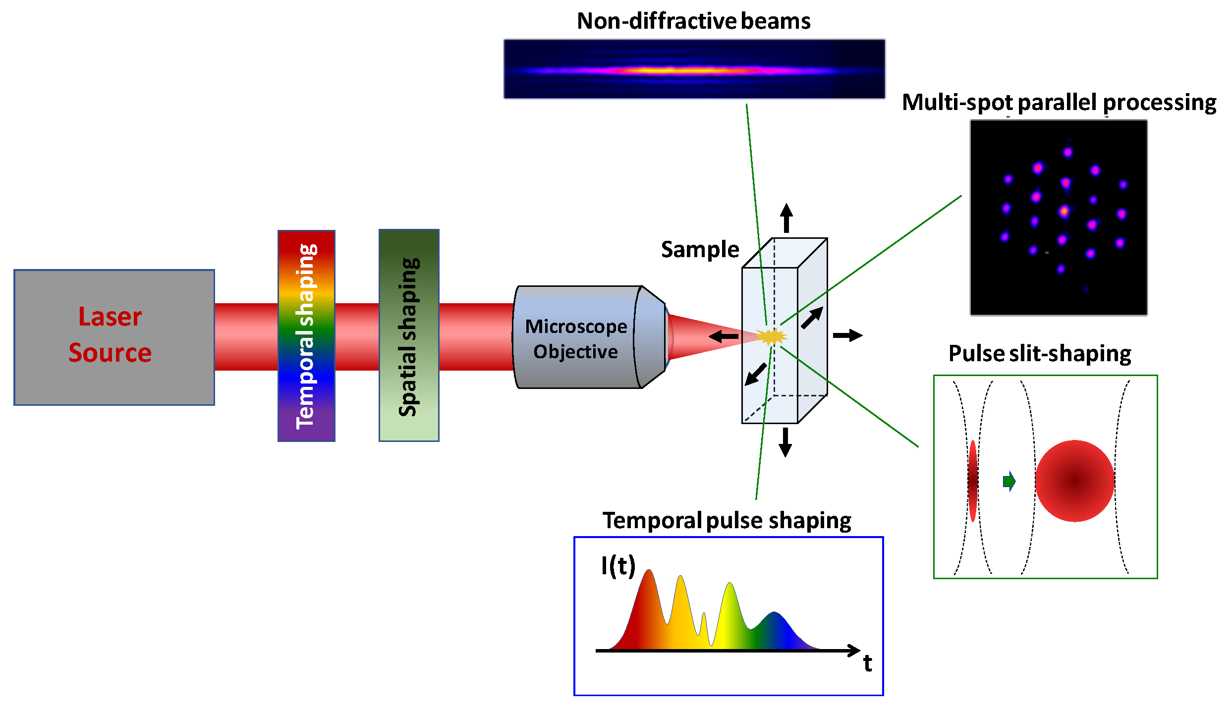
3. Irradiation Laser Sources and Methods

Mainly two types of laser sources have been utilized for the studies presented in this manuscript: (1) An amplified Ti:Sapphire femtosecond laser system delivering 800 nm light pulses with a maximum power of 600 mW and a duration of 160 fs at a repetition rate of 100 kHz was employed as irradiation source mainly for DLW of glass samples. This source is equipped with a pulse envelope control unit in time based on programmable spectral phase modulation in liquid crystal arrays so the temporal duration of the writing pulse can be tuned as a function of the response of the samples. (2) An 800 nm amplified Ti:Sapphire femtosecond laser system delivering light pulses with a maximum power of 3 W and a duration of 50 fs at a repetition rate of 1 kHz, allowing equally for extraction of single pulses or controllable pulse sequences, was employed for time-resolved studies.
Glass exposure doses (pulse energy multiplied by the exposure time and the laser repetition rate) were controlled by electromechanical shutters. The beam was focused inside the target principally by large numerical aperture microscope objectives (NA = 0.42–0.45, effective NA due to truncation limited to NA = 0.4). Static and dynamic writing was performed by translating the sample using xyz motorized stages. A positive optical transmission (OTM) and phase-contrast microscope (PCM) inserted in the irradiation setup was used to image the interaction region in side-view geometry. In PCM, positive refractive index changes relative to the background matrix appear dark on a gray background, while white zones indicate negative index variations. The guiding properties of the photo-inscribed waveguides were verified upon injection with IR light. The level of local energy accumulation and the characteristic effect of local energy relaxation depend strongly on focusing conditions and the parameters of the laser pulse, as the duration, wavelength, repetition rate, as well as on the spatial features of the beam. Considering the presence of a band-gap of several eV, multiphoton processes are likely the most probable photoionization mechanisms [35]. In ChG glasses the band-gap is such that two-photon ionization is the predominant process for free carrier generation. Other processes, particularly free electron heating and subsequent collisional ionization can set in for pulse durations exceeding 100 fs and near-infrared or visible wavelengths. Therefore, the pulse duration can be seen as a key parameter for determining the laser-material coupling efficiency. The adjustment of pulse duration, with given laser fluence and repetition rate, can tune between positive Type I and negative Type II index changes. These processes may be further enhanced depending on the irradiation fluence and repetition rate, switching between low and strong thermal accumulation regimes, forcing thus thermal elements and phase transitions alongside cold structural arrangements in index modifications [36,37,38,39,40,41,42,43]. Equally, the index change depends on the nature of the glassy materials; their electronic, structural, and thermomechanical characteristics; where excitation and heating cycles may trigger densification or rarefaction [40]. During laser-material interaction, the local exposure level is also critically influenced by nonlinear propagation (particularly self-focusing) and light interaction with carriers (absorption, scattering) [41,42,43]. The control of the spatial and temporal envelope shape of the laser pulse can have therefore a strong impact in achieving significant control in regulating refractive index. This can be obtained by programmable tools capable to reconfigure in space and time the laser pulse using spatial and spectral phase modulation (see for example refs. [44,45,46]). Furthermore, inserting adaptive control feedback loops can achieve a synergetic interaction between light and matter [40]. Figure 1 gives a conceptual example of an irradiation tool with spatio-temporal beam engineering capabilities, where the ability to achieve non-diffractive propagation, focal shaping, or time-domain envelope design are powerful control knobs for laser irradiation, regulating thus excitation mechanisms, nonlinear propagation and the photo-inscription performance. This offers thus a dual perspective, of a phenomenological and a geometrical control of the exposure geometry via spatial design. For instance, spatial pulse shaping is a key concept for generating waveguides with large diameter cross-sections [7,47,48] and non-diffractive Bessel–Gauss beams for the photo-inscription of elongated high aspect ratio void-like nanostructures [49], both very important building blocks of efficient complex optical functions working in the MIR (a detailed description is given in the next sections).

4. Writing LMA Waveguides in ChGs for Light Guiding in the MIR

The requirements of single mode guiding in the MIR domain impose constraints on minimal waveguide section diameters (with ranges in the tens of µm) and index contrast (approaching or exceeding 10−3). In response to these limitations mainly two approaches have tested, namely the slit-shaping method [47,48] and the evanescently coupled multicore waveguide bundle design [7,9].

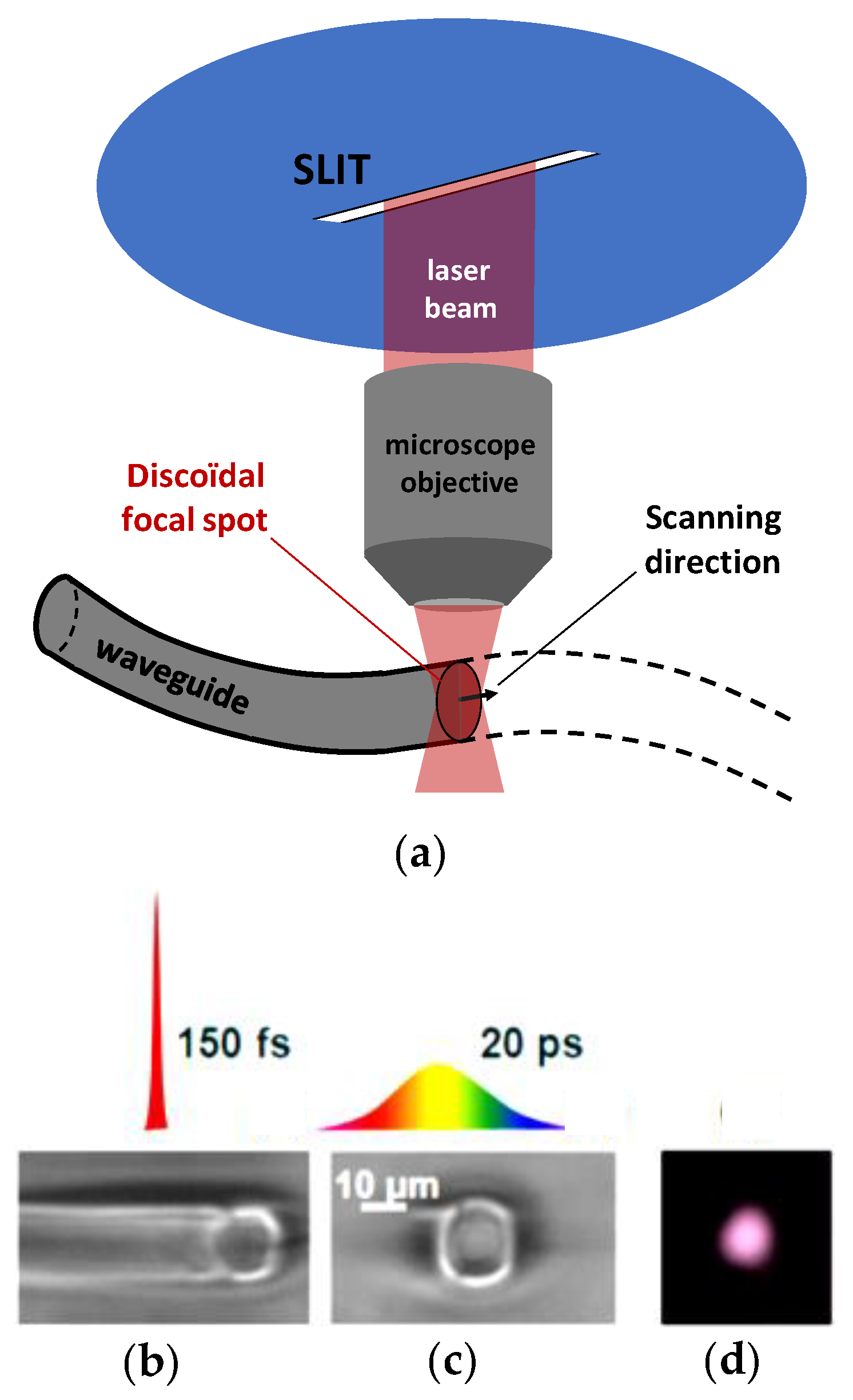
4.1. LMA Waveguide Photo-Inscription by Using Slit-Shaping Technique

In standard irradiation conditions, laser photo-inscribed waveguides have transverse cross-sections with few micrometers in diameter, and, particularly for transverse scan schemes, the cross-section is asymmetric and elongated in the direction of the confocal axis. One of the most effective spatial shaping techniques by which one can obtain either a higher symmetry of the transverse profile (increasing the circularity of the guided mode and reducing polarization sensitivity) or a larger cross-section diameter is the slit-shaping technique, allowing to change the profile along the propagation axis and thus the confocal volume. The technique has been introduced by Cheng et al. [47] using partial beam truncation along one transverse direction, and then reinforced via astigmatic control by Osellame et al. [48]. As a consequence of Gaussian beam propagation laws, decreasing the initial beam waist along one transverse direction leads to the related increase of the corresponding focal waist in the focal plane up to the point where it becomes comparable to the confocal length. A quasi-circular symmetry thus can be obtained in the form of a disk that can be replicated by transverse scanning to form a waveguide of larger diameter and circular cross-section. A conceptual schematic of the technique, and its utilization for waveguide photo-inscription, is presented in Figure 2a. The nonlinear propagation effects on the stability of the discoidal focal spot were recently discussed [50], showing a certain robustness of the technique [51] and good optical performances in terms of losses, typically below 1 dB/cm. For high nonlinear glasses such as ChGs an ultrashort pulse duration leads to strong nonlinear distortions before the focal point. McMillen et al. [52] have shown that slit-shaping techniques can be applied to high index nonlinear materials such as GLS glasses. It has been demonstrated that despite the presence of spherical aberrations and Kerr-nonlinearities, low-loss (0.65 dB/cm) waveguides can be obtained with pulse durations around 1 ps.
An example of slit-shaping waveguide results with modal outputs upon near-infrared injection is given in Figure 2b,c for a Ge15As15S70 sample. Ge15As15S70 glass has higher nonlinear susceptibility than GLS and ultrashort pulse propagation at higher energies, as required in slit-shaping methods, which is unstable against filamentation and self-focusing, and they are even more distorted than in GLS. This is becoming apparent in Figure 2b, which shows extended damage around the slit-shaped core. However, it has been shown that increasing the pulse duration to 20 ps can restrict the collateral damage and confine the radiation around the slit shaping zone. This is due to a downsize of the Kerr self-focusing and carrier defocusing along the propagation path allowing to deliver the main energy in the interaction region. The result is given in Figure 2c with the corresponding behavior of single mode guiding at 800 nm showed in Figure 2d. The typical transverse dimensions obtained by this technique are in the range of 10 µm; longer confocal distances (lower NA objectives) can in principle generate larger cross-sections; however, this requires increasing the focused power and therefore this configuration is unstable, as susceptible of very high nonlinear deformations.

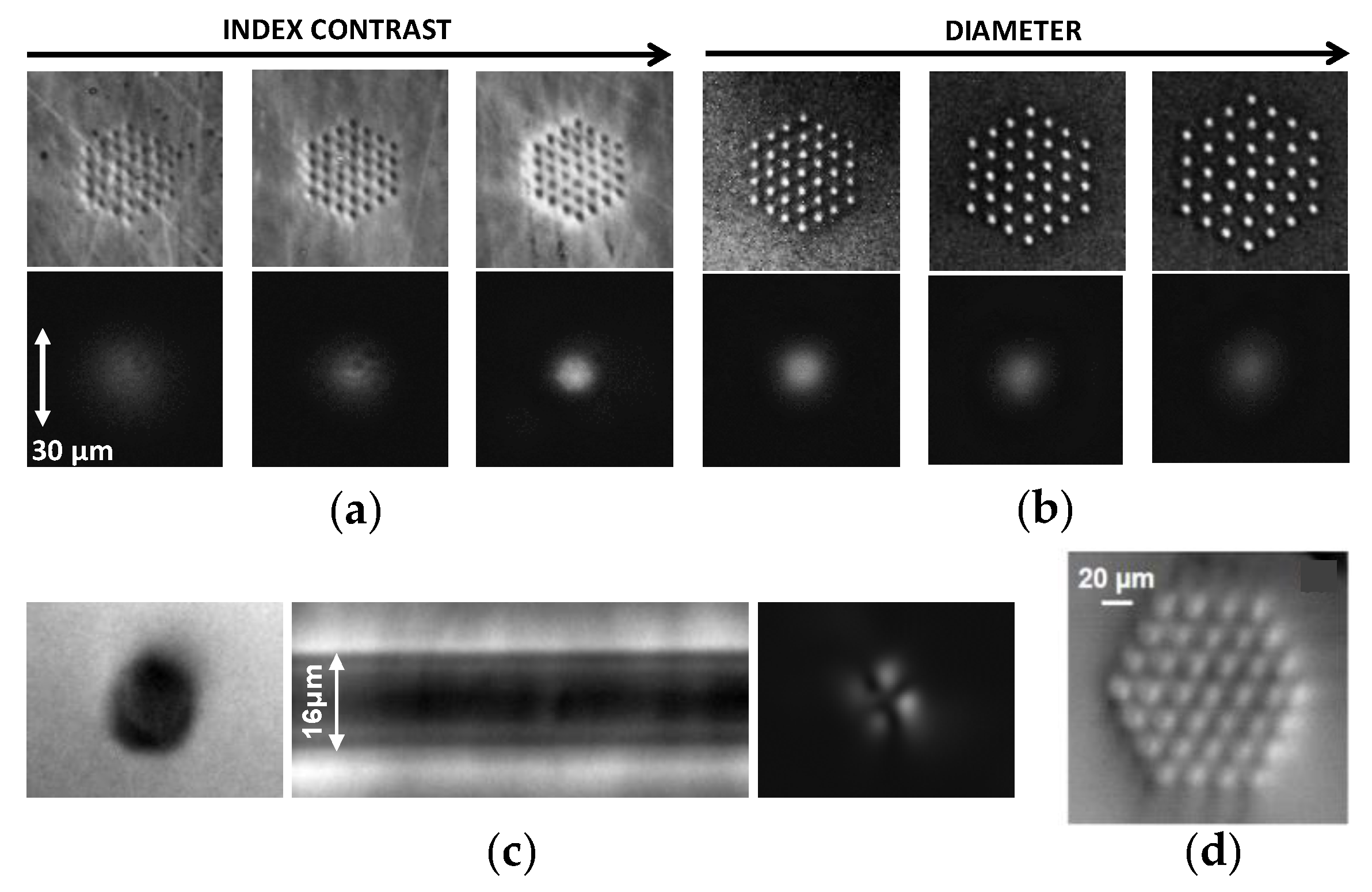
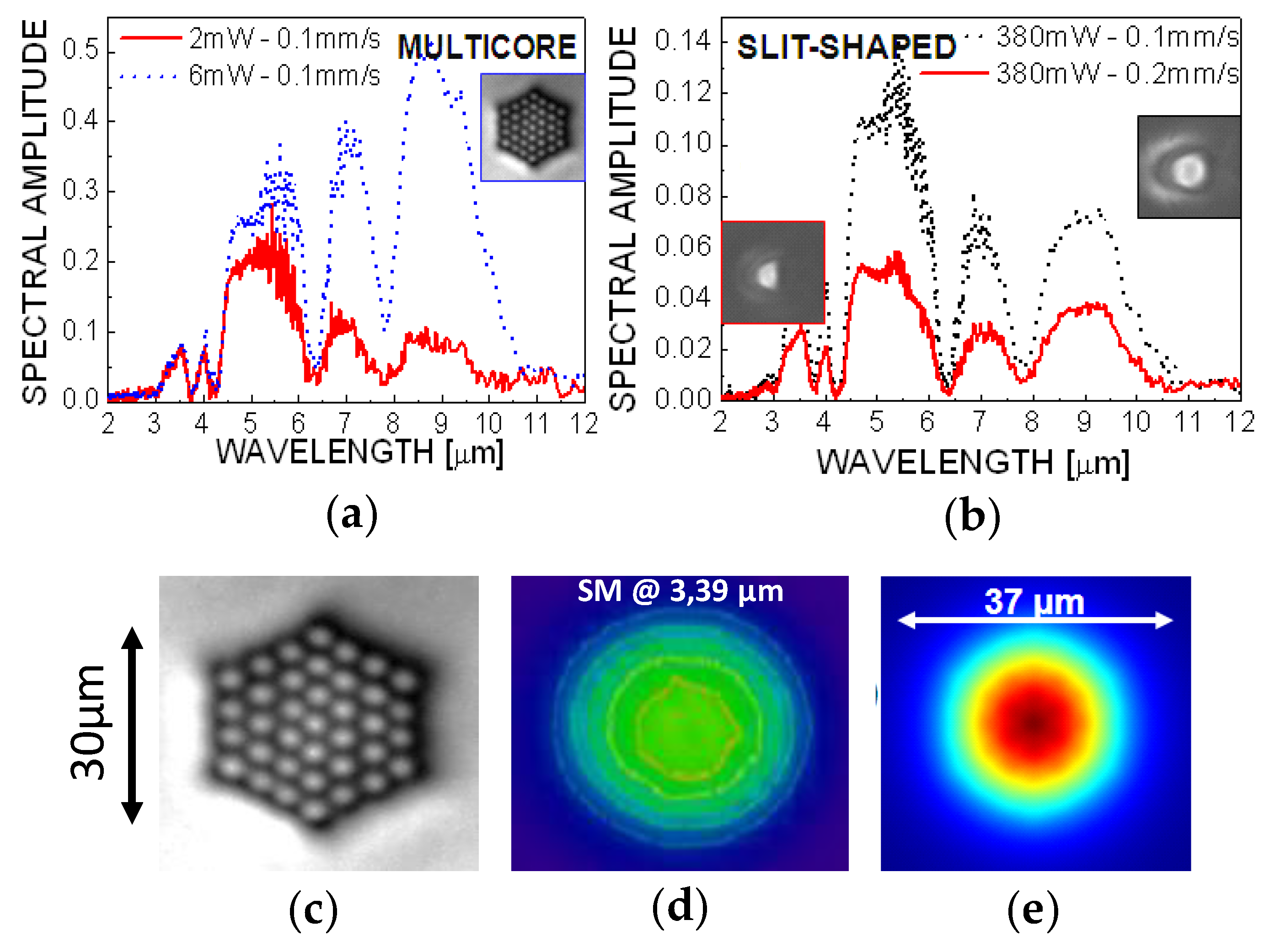
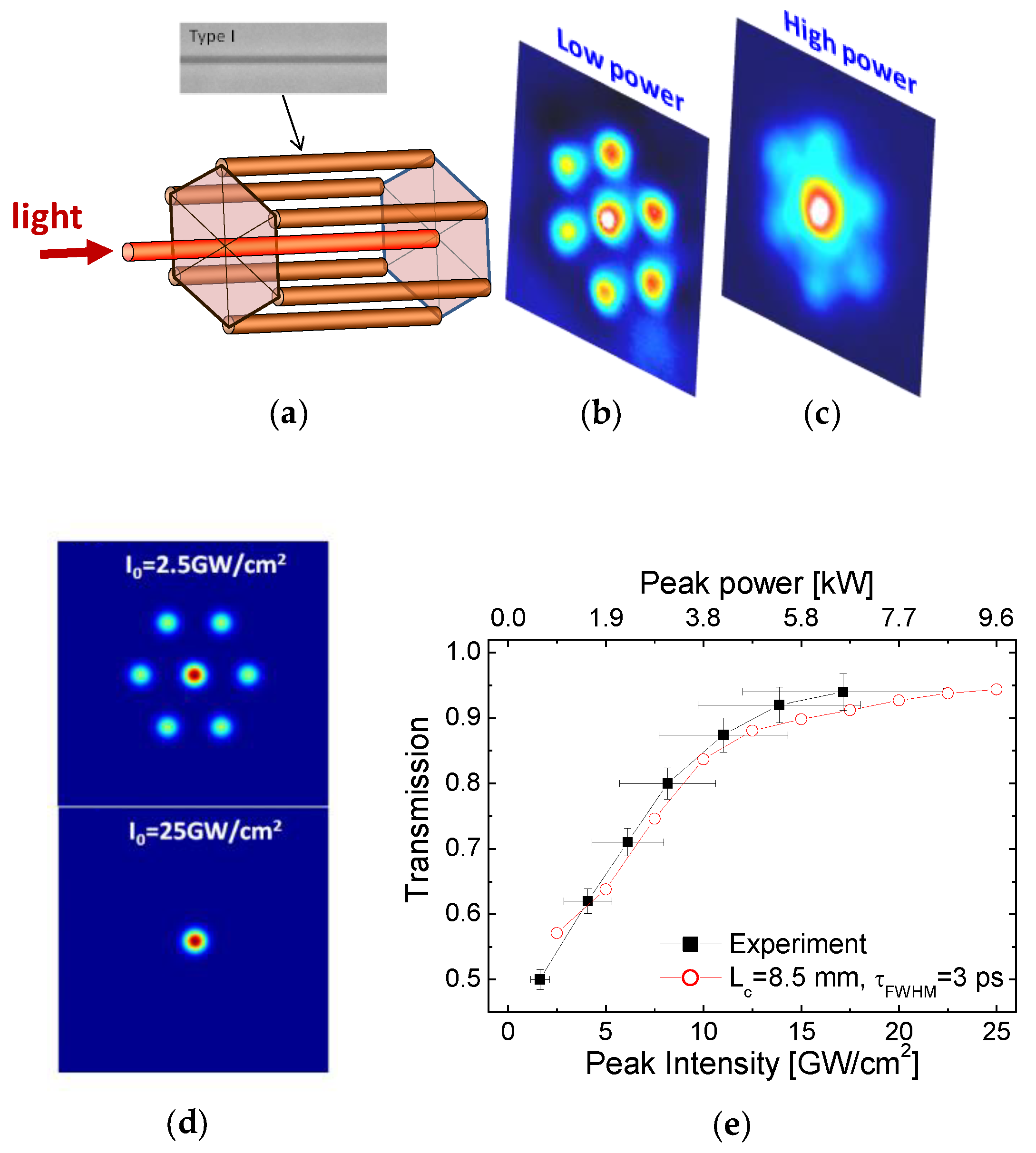
4.2. LMA Waveguide Photoinscription by Using a Multicore Array and Evanescent Coupling

Further flexibility in the normalized frequency requires increasing even more the waveguide cross-section diameter, beyond the typical limit of the slit-shaping technique. The flexibility in designing optical functions in a waveguide array concept is considerable, ranging from photonic crystal fibers to imaging devices, routers, and mode convertors [53,54,55]. In the context of LMA light transport, evanescently coupled fibers [56] or embedded waveguides [47] were demonstrated to be potential efficient solutions. The coupling efficiency in waveguide arrays is the key engineering factor in designing the properties of the array, and it can straightforwardly be designed using index contrast, inter-trace spacings, or lengths for various spectral domains. In terms of optical guiding, based on a multicore fiber concept, a matrix of waveguides permits upon central injection and gradual coupling in the next neighboring waveguides the development of in-phase modes that will coherently overlap, thus forming a large-area single mode covering the whole array. An example of photo-inscribed multicore array waveguides functioning in single-mode operation is given in Figure 3a,b. Typical hexagonal arrangements with 37 micron-spaced 10 mm-long traces were used in a Ge15As15S70 sample. For typical single trace NA below 0.05, equivalent to index contrasts of up to 5 × 10⁻⁴ at 800 nm, the individual modes superpose coherently and create super-single-mode propagation over the bundle cross-section. Higher NA and/or section diameters lead to stronger mode localization and favorable conditions for multimode guiding. Results given in Figure 3a,b indicate the role of index contrast and structure size on mode confinement. The mode becomes more confined when increasing the index contrasts and keeping the diameter constant (Figure 3a), or inversely can be extended with larger inter-trace separation and keeping the index contrast constant (Figure 3b). Consequently, the single trace NA can be adjusted for single mode conditions, with losses around 1 dB/cm. Overlapping traces create uniform structures of circular symmetry which behaves multimode at 800 nm, with the onset of the LP21 mode (Figure 3c). Even larger sections (up to 100 µm or more) with multimode character can be obtained using multicore bundles with slit-shaped individual traces (Figure 3d).

4.3. Guiding MIR Light in Bulk ChG Glasses

Tests of MIR light guiding with multicore and slit-shaped structures with index contrasts up or in excess of 10−3 are given in Figure 4. The results indicate high transmittance over the whole black body source range (2–13 µm) convoluted with the glass transparency window (0.5–11 µm) and the detector response (FLIR camera). The large band response in Figure 4a shows chromatic effects with apparent slightly higher attenuation at large wavelengths depending on the degree of mode confinement, obtained by increasing the waveguide index contrast. The chromaticity of the structures can be controlled via index contrast engineering. Chromatic effects are less apparent in slit-shaped traces (Figure 4b), with main index contrast effects in the overall guide transparency. Spatial mode profiles under coherent light injection were tested at 3.39 µm He-Ne laser radiations for multicore structures and show symmetric single mode guiding (Figure 4d) with mode areas matching the size of the multicore structure in Figure 4c. The result is confirmed by numerical simulations (details can be found in ref. [9]). An example of a calculated mode is given in Figure 4e for a hexagonal structure having the same characteristic of the experimental one. The guiding performances were experimentally analyzed via the cut-back method on multicore guides of several lengths, indicating propagation losses in the 1 dB/cm range at 3.39 µm injection. More recently, Masselin et al. [34] showed that propagation losses as low as 0.11 dB/cm at 1.5 µm can be obtained by optimizing the index contrast of multicore structures in bulk ChGs.
Other techniques and configurations have been proposed in the literature in order to increase the guiding cross-section area. These techniques are mainly based on depressed cladding concepts [16,57,58] (photo-inscription of a low index Type II cladding surrounding the guiding area), or on a 1D version of the multicore concept [59] (periodic arrangement of Type I index slabs). In particular, depressed-cladding techniques can be effective in bulk materials which cannot sustain contrasted Type I index structures, as is the case for example in As2S3 chalcogenide glass, as will be discussed below.

5. Study of the Response of ChGs to Ultrafast Focused Laser Beams

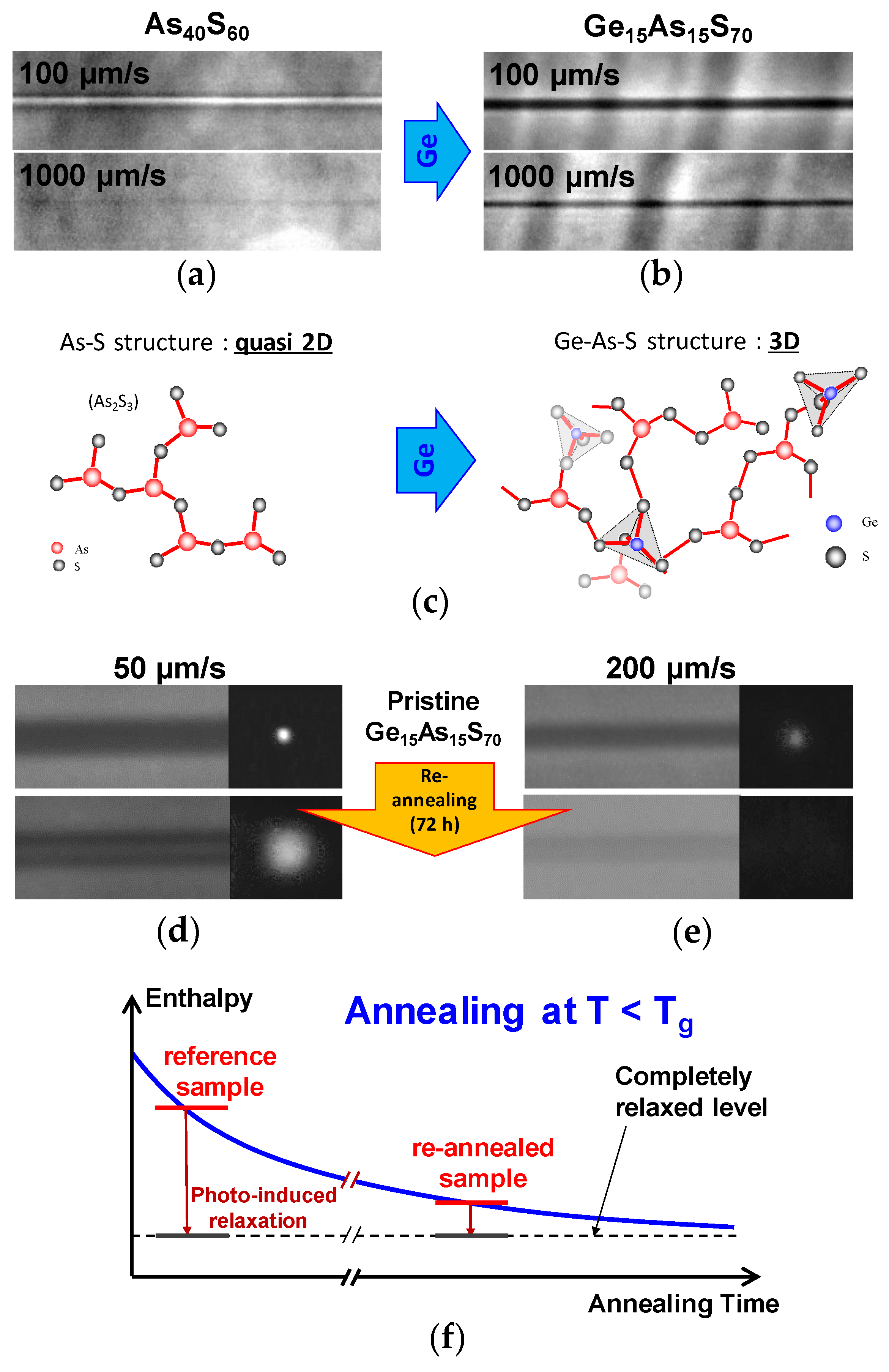
5.1. Role of Glass Elemental Composition and Thermal History

As mentioned before, the final result of the laser-induced local index change in ChGs strongly depends on the material reaction to the focused laser pulse. The first fundamental role within the material-laser coupling mechanism is played by the microscopic glass molecular structure. Here the role played by the glass elemental composition is evidenced by comparing the optical response of two ChGs, namely As2S3 and Ge15As15S70, under femtosecond laser irradiation. Typical photo-inscribed longitudinal waveguides, obtained by translating the sample in the confocal direction during laser irradiation, are shown in Figure 5a (As2S3) and Figure 5b (Ge15As15S70). The irradiation conditions were the same for the two glasses, with a laser energy density (in vacuum) at the center of the focal region reaching about 130 J/cm3. The waveguides were photo-inscribed at 100 kHz repetition rate, using two different translation speeds: 100 µm/s (top) and 1000 µm/s (bottom). As can be clearly seen, As2S3 and Ge15As15S70 samples show an almost opposite response. The result can be summarized as follows: (1) As2S3 presents mainly Type II negative refractive index modifications; positive index Type I modifications are observed for very low laser doses (low power and/or high translation speeds) in a relatively narrow range and with a very poor contrast; (2) Ge15As15S70 presents mainly Type I refractive positive index modifications over a wide range of laser dose values (Type II modifications are observed, but only at relatively high laser doses). A first conclusion can therefore be given here. Doping with Ge an As-S glass structure, having very narrow windows for Type I index modifications, allows creating glasses (Ge-As-S structures) with a large window for Type I index modifications, which is much more suitable for photonic applications.
Observing the role of Ge in establishing a wide window of positive index changes, a question can be addressed: How the structural flexibility of the As-S and Ge-As-S glass structures is related to Ge insertion? A first remark can be done here, the quasi planar As-S molecular structure acquires a 3D connectivity after inserting Ge, as depicted in Figure 5c; one can claim therefore that this is a key factor to increase the level of structural flexibility. Moreover, several levels of structural arrangements and rigidity of the glass matrix can be obtained depending on the thermal history during glass preparation. The glass thermal history is a key factor in establishing the link between the matrix connectivity and the degree of photo-induced densification. Here, two distinct regimes are compared: a short annealing close to the glass transition temperature Tg, as the glass exits from the laboratory standard synthesis procedure (in the following called the “reference” or “pristine” sample), and a long re-annealing (in the following called “re-annealed sample”), both followed by a slow ramped cooling. The process by which Ge-As-S glasses are prepared generates quite unrelaxed glasses with characteristic volumes higher than the volume corresponding to a relaxed configuration, and therefore a lower density. Re-annealing should enable a structural relaxation process that corresponds closely to a structural equilibrium at the annealing temperature, little affected by the cooling tie as the relaxation times becomes prohibitively long [60]. In other words, from a standard normal thermodynamic behavior of a chalcogenide glass, the longer the annealing time at temperatures under Tg, the lower its final volume, i.e., the higher its density [61], as schematized in Figure 5e. The glass refractive index, which depends on its density, will depend therefore on its thermal history. A glass annealed for a long time at a temperature close to Tg will have therefore a higher refractive index than a glass annealed for a short time; global refractive index variations of the order of 10−4 to 10−3 can be achieved by annealing [62,63]. The enthalpy represents a first evaluation of structural flexibility allowing evaluating the strength of additional laser-induced modification on a structure with different degrees of relaxation, up to the point where, in principle, no further structural changes and relaxation can be induced. In re-annealed samples, where the glass structure is relaxed, it should be much harder to induce photo-contraction, and furthermore the opposite effect of photo-expansion should be observed, especially at higher intensities [64]. To verify this point, ultrafast laser photo-inscription of Type I waveguides has been performed in two samples, a reference Ge15As15S70 glass, as prepared in the laboratory with a standard procedure, and a similar sample but re-annealed during 72 h at Tg–15 °C and then slowly cooled to room temperature. The photo-inscription process was performed in both samples under the same experimental conditions and the response of the two samples was evaluated by performing guiding tests (injecting light in the waveguides and evaluating the intensity of the near-field guided modes at the exit). The results are shown in Figure 5d,e, the response of the reference and re-annealed samples was significantly different. The reference sample (top) showed the expected response, a good photo-induced local densification and a good confined guided mode, while waveguides photo-inscribed in the re-annealed sample (bottom) showed a much lower index contrast with a poor guided mode. Furthermore, as can be seen on the bottom of Figure 5d, in the re-annealed sample, the region where the laser pulse is more intense (the center of the pulse) gives an inverted response, with a negative refractive index variation. This behavior was expected and it is in good agreement with the results reported in [64], i.e., irradiating the surface of high enthalpy chalcogenide glass with low intensity laser pulses results in a large photo-contraction, while high intensity irradiation can generate the exactly opposed effect, i.e., photo-expansion, in low enthalpy samples. These results can be explained in terms of volume reduction by structural relaxation when high enthalpy ChGs samples are annealed for a long time slightly under Tg.
Raman shift analysis performed on non-irradiated and irradiated Ge15As15S70 samples showed many molecular structural changes corresponding to the irradiated region, among which a reduction of the number of As-As bonds, with S8 rings and small chains partially replaced by S-S bonds connecting AsS3/2 and/or GeS4/2 entities [65]. This is a signature of an augmented disorder under laser irradiation, and a possible cause of photo-induced densification. Measurements on re-annealed samples showed qualitatively the same behavior; the same molecular changes after laser exposure were observed, but were less intense than in the case of non-reannealed samples, in agreement with the difference observed in the refractive index change. Recently, Gretzinger et al. [66] reported on structural rearrangements and ion migration in correspondence of Type I structures photowritten in GLS, as evidenced by Raman spectroscopy.
Based on all the results presented above, the following scenario has been proposed. First, the insertion of Ge in a quasi-planar As-S matrix introduces a 3D connectivity and new degrees of freedom, allowing for higher structural flexibly and so a higher relaxation potential. One could think that it is more difficult to relax a planar structure such as As2S3 than a 3D connected structure such as Ge15As15S70. This indicates that the laser role is to trigger locally states with a different degree of relaxation with respect to the pristine sample, inducing further relaxation in unrelaxed or partially relaxed matrices (with a result in index increase) or to induce structural constraints in relaxed matrices up to thermomechanical effects (local expansion). The question is then how the laser pulse is able, via the deposited energy, to trigger molecular mobility and structural rearrangement [67]. As a consequence of the ionization of the sample by the focused laser pulse, a number of electrons are promoted from the valence band to the conduction band by two-photon absorption. When electrons are excited to the conduction band, covalent bonds of the glass matrix are weakened and molecular mobility is allowed even at room temperatures where normally it is prohibited by slow kinetics. The lifetime of the electron plasma generated by a single pulse (which can reach few tens of nanoseconds [68]) is too short to induce an efficient molecular mobility with only one laser pulse; however, following laser pulse after laser pulse, a relaxation channel is generated through which the glass structure is allowed to rearrange even at room temperature. The irradiation process can be seen therefore as a way to remove the kinetic constraint to the thermodynamically driven relaxation. These results are in good agreement with previous works reported in the literature. Hisakuni and Tanaka [60,69] reported on photo-induced glass softening effect in amorphous As2S3. They have shown the possibility of a-thermally photo-induced fluidity, i.e., the possibility of introducing degrees of freedom and structural mobility via paths that are not exactly temperature driven in the glass matrix under laser irradiation. More recently, Lucas and King [67] reported on the observation of fast light-activated relaxation in GeSe9 chalcogenide glass illuminated with sub-band-gap light from a Ti:Sapphire laser.

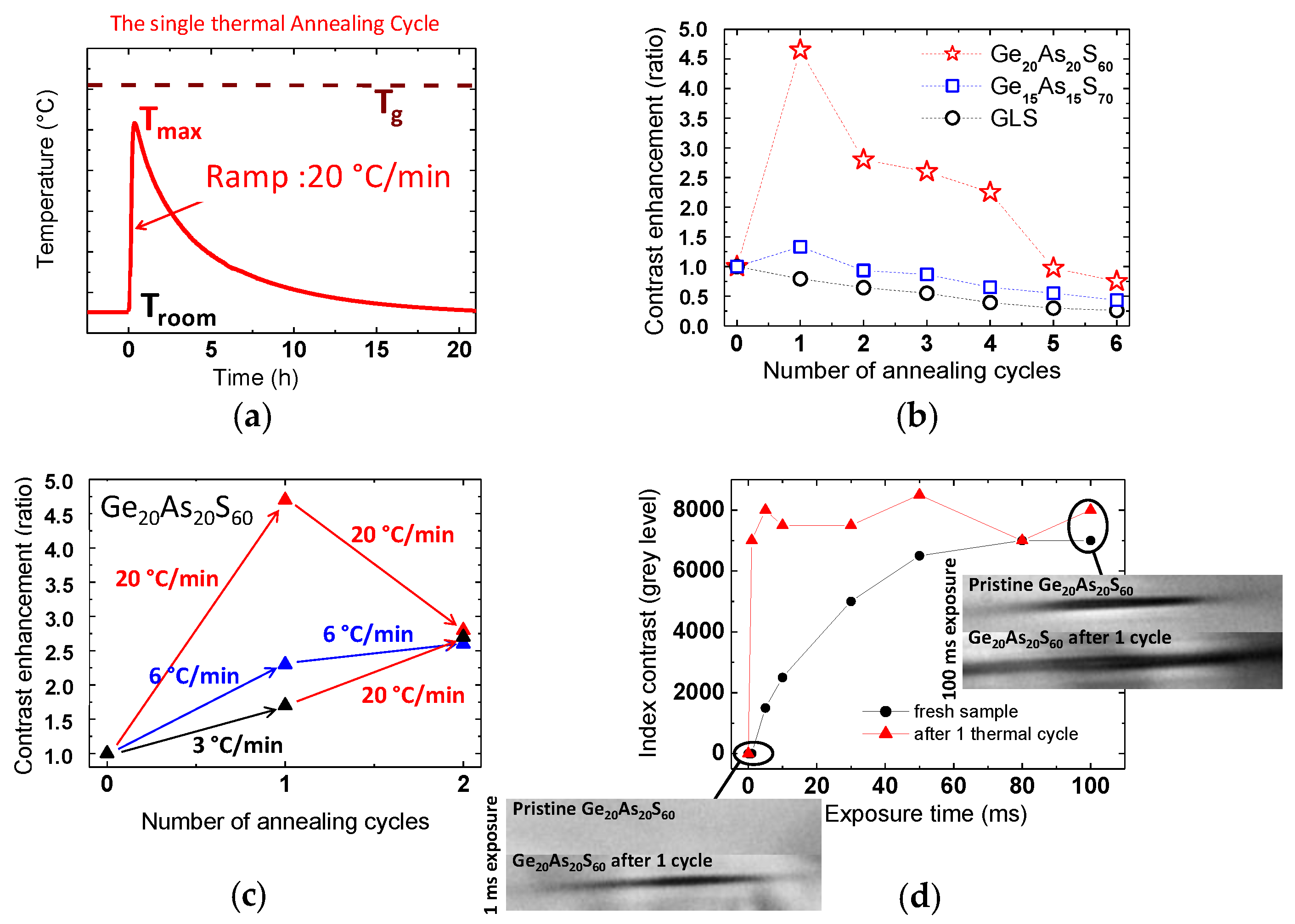
5.2. Unexpected Behavior of Ge-As-S Glasses under Short Thermal Annealing Cycles

Because the laser induced densification, and therefore the index contrast, increase with the number of laser shots, this means that there is a threshold in terms of laser dose at which the photoinduced index contrast starts to be visible in PCM (this threshold can be estimated as slightly under 10−4). The existence of this threshold for laser-induced densification is related to how the laser pulse couples with the microscopic glass matrix, determining thus the degree of nonlinear photosensitivity. On the other hand, the laser-induced index contrast saturates at high laser doses. This is due to the fact that in correspondence of the regions where the positive index contrast has reached the maximum value, the glass cannot further densify and it starts to expand instead, when the laser dose is increased. The saturated value of the index contrast depends on the specific glass and, in particular, on its structural flexibility, as discussed before. These features indicate that, comparing the laser-induced index contrast before and after a thermal pretreatment allows understanding the action of the pre-treatment on the glass matrix (glass thermal history). In particular, it allows distinguishing between a thermally induced physical aging due to enthalpy relaxation, as discussed previously, and a thermally induced modification of the molecular polarizability (generation of new molecular entities and/or point defects, having ionization energies lower than the glass band-gap). The latter will induce weakness points acting on the coupling efficiency between the laser and the glass matrix, rather than on the densification threshold of the glass structure. To clarify this point, a study of the change of the response to focused laser pulses of three ChGs, namely Ge15As15S70, Ge20As20S60, and GLS, after short annealing cycles, has been performed. The single thermal annealing cycle is detailed in ref. [70] and shown in Figure 6a. The slow cooling allows relaxing the mechanical stress eventually accumulated during the “fast” heating process to a temperature Tmax < Tg. The relative variation of the local densification induced by the focused laser pulse after each annealing cycle has been analyzed, after each annealing cycle, and the result is shown in Figure 6b. For fixed laser irradiation conditions (laser parameters and focusing geometry as given in ref. [70]), the photo-induced index contrast may show a non-monotonic variation, cycle after cycle, and, in particular, it may show a drastic variation after the first short annealing cycle, as in the case of Ge20As20S60 sample (red stars), for which the photoinduced positive index contrast increases by 4.7 times its initial value. Because the laser irradiation parameters were maintained constant during the experiment, this means that the efficiency of the process by which the focused laser beam induces local densification can be considerably enhanced by thermal pretreatment of the sample (short annealing under Tg) before laser irradiation. The same trend is showed by Ge15As15S70 glass (blue squares), excepted that in this case the index contrast increases only by a factor 1.3, after the first annealing cycle. On the contrary, the GLS sample (dark circles) showed an opposite behavior. Laser-induced positive index contrast in GLS has a monotonic decreasing behavior, cycle after cycle, with respect to its initial value. The effect induced by the thermal pre-treatment on all the tested samples is stable in time; it has been verified in fact that by photo-inscribing again the samples months later, in the same experimental conditions, the thermally induced effect was unaltered.
A typical thermally induced structural relaxation of the glass matrix (physical ageing, entropic process) is expected to be monotonic as a function of the annealing time. This is the reason why, if the behavior observed in the case of GLS was expected, the non-monotonic evolution, cycle after cycle, observed in the case of Ge15As15S70 and Ge20As20S60 is a surprising and unexpected result. To solve this apparent paradox, one can claim the activation of a new mechanism during the glass short thermal pretreatment. Experimental evidence in favor of a new non-entropic relaxation channel activated by the thermal treatment was obtained by analyzing the response of the Ge20As20S60 sample to laser radiation during the two first annealing cycles, as a function of the heating rate, by maintaining the maximum temperature, Tmax, constant. The result is shown in the graph of Figure 6c. In this graph one can see that the strength of the thermally-induced enhancing effect strongly depends on the value of the heating rate (the higher the rate the stronger the effect). The volume relaxation by physical aging when a glass sample is annealed under Tg is an entropic process and cannot depend on the slope of the heating ramp. Moreover, the graph of Figure 6d shows the variation of the laser-induced index contrast, in the Ge20As20S60 sample, as a function of the exposure time (with constant laser average power and duration), before (dark solid circles) and after (red solid triangles) the first annealing cycle. The change of the response of the sample to the laser radiation, before and after the thermal treatment, is evident. One can remark in this graph how the response shows a big change at low exposure times, while the saturation value of the index contrast at higher exposure times remains almost the same. In other words, after the first annealing cycle the response of the sample to laser radiation (in terms of induced index contrast) saturates much faster as a function of the laser energy dose, but the saturation value of the index contrast remains almost unchanged. This is a clear observation of the effect induced by pre-annealing the sample, namely an increase of the glass nonlinear photosensitivity. This effect is directly observable in the inset on the bottom left of Figure 6d, corresponding to the case of low laser exposure time. All these results are a clear indication of the fact that the non-monotonic relaxation of Ge-As-S glasses matrix during a thermal treatment is the result of two competing mechanisms; one is the well-known monotonic entropic relaxation of the microscopic glass structure with the annealing time (physical aging); the second mechanism, which depends on the heating ramp and is responsible for an enhancement of the glass nonlinear photosensitivity, is a new relaxation channel activated by the thermal treatment. Furthermore, it has also been verified that the glass band-gap keeps unaltered after each annealing cycle, excluding an enhancement of the two-photon ionization efficiency. The generation of mechanical stress during the annealing cycle and then relaxed by the laser, is also a mechanism, which can be excluded because the sample has enough time to relax the stress during the slow cooling process. A few similar examples are reported in the literature for bulk fused silica. In the case of fused silica, the lowering of the photo-inscription threshold is obtained by loading the sample with hydrogen (H2) or by pre-irradiating the sample with X-ray radiation before laser irradiation [71,72,73]. In the latter case, the lowering of the photo-inscription threshold can be attributed to the fact that pre-irradiating the sample with X-rays generates point defects (NBOHC), which are considered as precursors of the laser-induced local densification process in bulk fused silica [5]. In the present case of thermal pre-treatment of Ge-As-S samples, by analogy, the laser photo-inscription enhancement could be attributed to a change in the molecular polarizability, with the generation of new molecular entities with ionization energies lower than the band-gap of the host glass and therefore easier to be ionized (weakness points). Another possibility is to consider more complex mechanisms involving the interaction between localized glass states and the environment (two levels system (TLS) model) [74,75,76]. At the moment, however, the mechanism remains unknown and further studies are needed in this sense (Raman and photo-luminescence studies on the laser modified region before and after thermal treatment). Anyway, the increasing of the glass nonlinear photosensitivity by a thermal pre-treatment can be considered potentially important for photonic applications because it can speed-up the laser photo-inscription process of bulk waveguides [70].

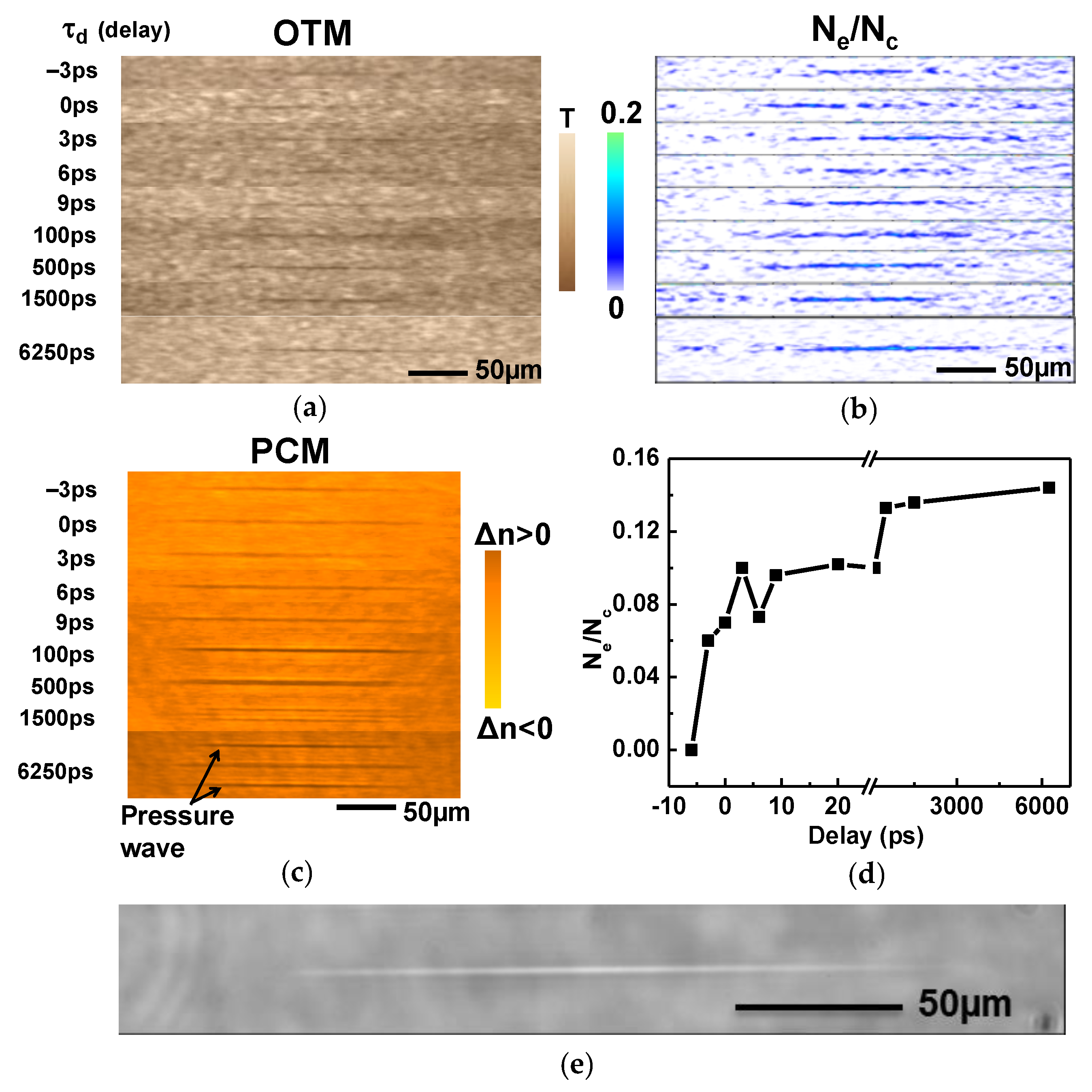
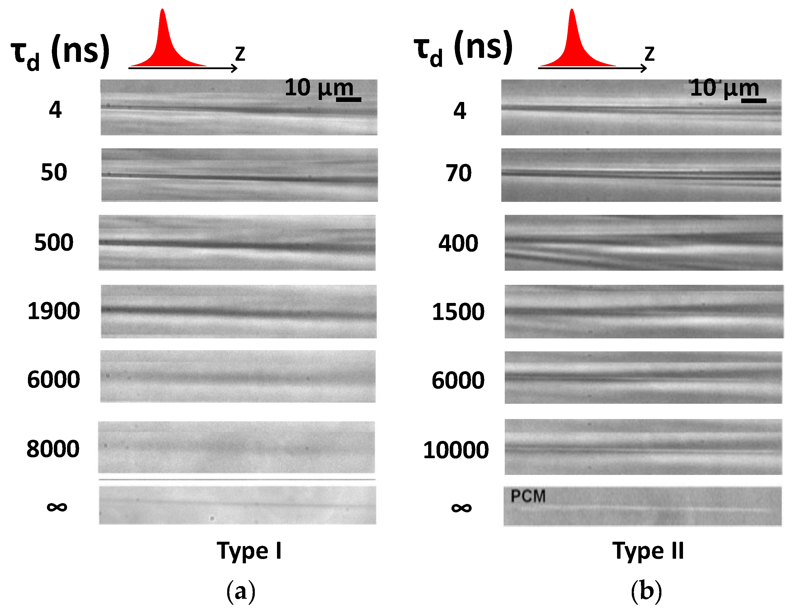
5.3. Time-Resolved Multi-Timescale Relaxation Dynamic

Time-resolved studies of the glass response to laser irradiation in single-shot regime have been performed in order to understand the role of the primary laser electronic excitation and the subsequent material thermodynamic response upon the genesis of Type I and Type II permanent changes in bulk Ge15As15S70 and GLS glasses. These studies have been performed in a single shot mode, where the incoming ultrashort laser pulse, which locally modifies the material, is shaped in a non-diffractive mode in order to generate Bessel–Gauss pulses [77]. Bessel beams are chosen because their quasi-non-propagative self-healing behavior allows locally deposing higher energy densities with reduced nonlinear effect due to propagation, as observed for example with Gaussian laser beams. The imaging setup is based on an optical microscope that can operate in optical transmission and in phase-contrast mode. The observation objective NA = 0.55 gives a spatial resolution of 530 nm at the observation wavelength. In a first experiment, the material dynamics from ps to ns timescales after laser irradiation is recorded by means of a standard pump-probe setup, where the probe is deducted from the pump, delayed with an optical delay line, and then doubled in frequency before being sent in the illumination path of the microscope [78]. Both phase contrast and optical transmission imaging were used in order to follow the evolution of the real (refractive index) and imaginary (free carrier absorption) parts of the material dielectric function after laser excitation. The situation described here concerns only the single-shot induced Type II index changes, because the excitation yield in Type I range was too low to observe carrier densities, leading to a belief that they may be below 1019 cm−3. The result shown in Figure 7 corresponds to the plasma generated by focused single-shot 4ps-long laser pulses with energy of about 1 µJ. The plasma relaxation detected by optical transmission as a variation of local transmissivity is shown in Figure 7a, while the relative optical phase variation detected by phase contrast microscopy is shown in Figure 7c. The electron density Ne, normalized to the critical density at 800 nm incident wavelength, has also been estimated [65], and its variation as function of the delay time between the pump and the probe beams is reported in Figure 7d. A long-living plasma, up to the ns scale, has been observed. A second aspect concerns the optical phase dynamics, relating to a local transient change of the refractive index. The results permit to link the transient index to a hydrodynamic behavior. The hydrodynamics initiated by laser heating is shown in the Figure 7c. Here, a pressure wave, travelling at about 6000 m/s, is clearly visible starting from a delay time of about 1 ns. The presence of this pressure wave indicates a thermo-mechanical relaxation of an initially hot region and a hydrodynamic expansion due to laser heating, and can explain the rarefaction and the associated negative index change observed corresponding to Type II modified regions (white traces in phase-contrast mode). The high negative refractive index contrast (high rarefaction regions, which can go to voids) obtained in this case in single shot regime (see Figure 7e) indicates a cavitation regime, which is reached after thermodynamic expansion in liquid phase. This suggests therefore that in this case, temperatures largely higher than Tg are reached locally in the sample. The behavior of the irradiated sample at lower energies however is completely different. No plasma has been detected and no pressure-waves have been observed in correspondence of generated Type I permanent positive refractive index changes. This indicates that in this case, the electron density is under the detecting threshold, and the local temperature of the glass matrix after carrier relaxation and vibrational excitation is not high enough (under Tg) to initiate a local hydrodynamic expansion, as observed for Type II permanent changes.
The complete relaxation dynamics up to µs timescale has also been observed using time-resolved phase-contrast imaging and non-diffractive Bessel beams. This time the study was performed in bulk GLS. The two-color pump-probe microscopy technique used in this case is different from the one described above, because in this case the probe pulse is obtained by using a random lasing effect, as described in [79], allowing to obtain a sequence of high-spatial resolution snapshots. The laser gain medium consists of a colloidal solution of Rhodamine B (2.5 g/L) with immersed latex nanobeads (of 325 nm size) at a concentration of 4 × 10¹⁵ L−1. The random lasing effect is obtained by irradiating the colloidal solution with 532 nm laser pulses (doubled Nd:YAG laser operating at 10 Hz) in its absorption band. Stimulated emission occurs where multiple scattering on the distributed nanobeads creates the random character. The random lasing effect is detected via the appearance of a strong spectral narrowing of the fluorescence band to around 13 nm bandwidth (FWHM) centered at 590 nm. Its pulse duration is similar to the excitation pulse in solution, i.e., 7 ns, which gives the temporal resolution of detection. A bright low-coherence illumination source has the potential of acquiring high quality speckle-free images, providing at the same time information on the amplitude and on the phase of the object. This illumination method increases significantly the dynamical range of the image and the signal-to-noise ratio. The electronic synchronization between the ultrafast laser system and the ns laser system ensures the time-synchronization between the exciting ultrashort laser pulse and the random lasing illumination (probe) source, with delays measured by a fast photodiode, permitting to correct for the jitter.
The result of the time-resolved imaging for Type I and Type II cases is shown in Figure 8, which presents the raw sequence of images of the interaction region at different times. The observed dynamics in ns-µs timescales is globally similar to that observed in fused silica and described in ref. [80]. Both Type I and II dynamics indicate the occurrence via laser excitation of a transient heat source, diffusion, and cooling. The result is dependent on the achievable energy density and results either in Type I positive permanent index contrast (as potentially resulting from bond-breaking and molecular mobility) or in Type II index changes where a thermomechanical process seems in place resulting in the opening of a cavity. For Type I structures (Figure 8a), the involvement of heat (after an excitation phase not depicted here) is signaled by the transient index increase (dark regions). Heat diffusion then appears, which can be visualized as a transient transverse enlargement of the dark zone, with a characteristic time of a few μs. This is in agreement with the characteristic heat diffusion time, of the order of w 2 / D , considering a thermal diffusivity of D = 0.1 mm2/s [65] and heat source transverse dimensions in the range of w = 1   µ m . The visualization of the heat flow is based on a strong thermo-optic effect in GLS. The temperature variation of the refractive index reads as d n = ( n / T ) d T , with a positive thermo-optic coefficient of +7.5 × 10⁻⁵ °C (more than seven times higher than in fused silica). After cooling, a permanent low-contrast narrow positive index trace remains, due to molecular structural modifications. The results indicate that, although considered as a-thermal, molecular structural modification processes at these low intensity regimes are nevertheless accompanied by heat.
The dynamics of the processes in the case of Type II index modification is given in Figure 8b. These structures are obtained by increasing the laser pulse energy and duration. The full-cycle monitoring technique reveals a more complex sequence of processes than for Type I. The two first sequences show a low-index phase in the middle of the transient structure, which is still present at 70 ns, recognizable by the white color phase shift in PCM. This can be attributed to the presence of long-living free electron plasma. Then, the excited plasma relaxes and the material goes into a higher index phase. At that moment the transient high contrast positive index change is characteristic of a hot phase (thermo-optic effect). It has to be noticed that a strong plastic deformation appears at the 400 ns snapshot. This kind of deformation is not observed in fused silica [80], and is probably due to an accumulation of mechanical constraints, which are then relaxed in a very fast timescale (<1 µs), as evidenced by the subsequent snapshots. The subsequent slow opening of the void (white trace) suggests that a liquid form is formed, undergoing cavitation. The final permanent void structure being the result of a competition between the slow cavitation opening and the cooling process, can have a characteristic transverse size well below the diffraction limit [80], because optics is no more involved. This indicates the importance of a material response in achieving structuring sizes significantly smaller than the wavelength and the capability of beam engineering in triggering and controlling such response and the associated relaxation dynamics.

6. Embedded Photonics in Bulk ChG by Ultrafast DLW

Having an optimal control of the material response to ultrafast laser radiation is the key factor for generating optimized Type I and Type II local index modifications. This type of index engineering facilitates the design of optical functions. In this section, we discuss how photo-written Type I and Type II structures (especially Bessel high aspect-ration nanostructures) can be arranged to generate high-resolution embedded spectrometers and interferometers for MIR Astrophotonic applications. We emphasize the possibility in the same optical system to transport, manipulate, and read-out optical signals.

6.1. High Spatial Resolution Integrated Spectrometers

Reducing the size and power consumption of detecting instruments has always been an issue for spatial astronomical applications. Nowadays, with the development of Nanosat projects, the possibility of achieving very high resolution in a very compact and light device gives waveguide optics a very broad field of application. A possible approach is to develop integrated spectrometers where the spectrum is obtained by Fourier Transform of a static interferogram, as proposed in the SWIFTS-Lippmann configuration [81,82]. In the present approach, the stationary wave is obtained by superposing the direct and backward guided modes of a simple channel optical waveguide, the latter being obtained without using a mirror but only Fresnel reflection at the waveguide output, exploiting the high refractive index of GLS waveguides. For sampling the stationary wave inside the waveguide, periodic nanodots of gold sputtered on the surface [83], or grooves obtained by Focused Ion Beam technology (FIB) [82], are typically utilized. For the first time, the classical nano-scattering centers, fabricated by time-consuming lithographic techniques, are here replaced by Bessel high aspect-ratio nanovoids photo-written by DLW perpendicularly to the waveguide [10] (the energy scattered by the periodic nanostructure, which is then used to sample the signal transported in the waveguide), as shown in Figure 9a,b. Periodic Bessel nanovoids with a transverse section below 500 nm (see the inset on top-right of Figure 9b) and an axial dimension above 150 µm, separated by 10 µm were employed. As a guiding element, a photo-inscribed LMA waveguide was used, in order to achieve large diameter mode guiding in the NIR and MIR with single mode characteristics. This was based on a centered hexagonal arrangement of 37 parallel waveguides, as described in Section 4. A view on the multicore waveguide cross-section structure and the corresponding guided mode at 1550 nm, with a diameter of about 20 µm, is shown in the top-left inset of Figure 9b. The trial was performed in GLS. The main interest of this technology is not only that the waveguide cross-section diameter and index can be adjusted in order to have single mode guiding at the desired wavelength, but also that the sampling nano-voids can be written in a very short time using DLW (few minutes) over the whole length of the sample (typically few cm, and this is highly suited in order to increase the spectral resolution), whereas classical techniques such as FIB or lithography take hours, and are limited to small lengths (typically 500 μm), requiring mask shifting in order to cover high areas. Moreover, the sampling nano-voids can be set at different depths in order to optimize interaction with the evanescent field of the waveguide, optimizing therefore the scattered signal, and finally their form factor can be easily changed, in order to modify the extraction efficiency and directivity [84]. This is a perfect demonstration of the high flexibility of the DLW technique in realizing compact embedded detectors, if compared to existing industrially mature lithographic techniques.
Theoretically, the static interferogram as seen by the sampling centers inside the waveguide is given by S ( m ) = cos ( 2 π m Δ L / Λ ) , where m is the order of the sampling center, Δ L is the distance between two neighbor sampling centers, and Λ = λ / 2 n is the period of the stationary wave, where n is the refractive index of the waveguide. Besides, in order to obtain high-resolution sampling lengths when several millimeters are demanded, this can be easily done by using DLW. Theoretical values for the obtained spectral resolution and spectral window are respectively R = 2 n L / λ and Δ σ = 1 / 4 n Δ L [81]. With a typical sample length of L = 10,000 µm (length of the sampling region), an effective refractive index n = 2.4 (GLS sample) we expect resolutions of R = 30,600 for λ = 1.5 µm. This gives an idea of the spectral resolution that can be obtained with this simple device. The spectral window at 1.5 µm would be Δ σ = 104   cm 1   ( Δ λ = 23.4   nm ) when the distance between the scattering nano-centers is Δ L = 10   µ m . A demonstration of information extraction from the guided signal in the waveguide is given in Figure 9c. In this case, the guided signal was monochromatic light from He-Ne laser at λ = 3.39 µm. To correctly sample the interferogram, one would need sampling centers at least with a separation distance of Δ L = Λ / 2 = λ / 4 n 370   nm at λ = 3.39 µm. However, in this case the sampling nano-centers were too far from each other (10 µm), and the resulting obtained image is a Moire interferogram, that can be used as a first guess of the spectrum of the source. In fact, by fitting the experimental data (black circles), a first guess of the central wavelength can be obtained, as the Moire fringes are extremely sensitive to the accuracy of the wavelength. A precision of δ λ = 0.2   nm can be obtained using an effective length of the detected area of 5 mm, as shown in Figure 9c. This means a spectral resolution of λ / δ λ = 17 , 000 . This result is the first demonstration of the feasibility of a 3D SWIFTS principle in the MIR region using laser writing for designing the waveguide and the sampling centers, and without the need of a total reflection (mirror) at the waveguide output, as the Fresnel reflectivity at the interface GLS/Air is of the order of 16%.

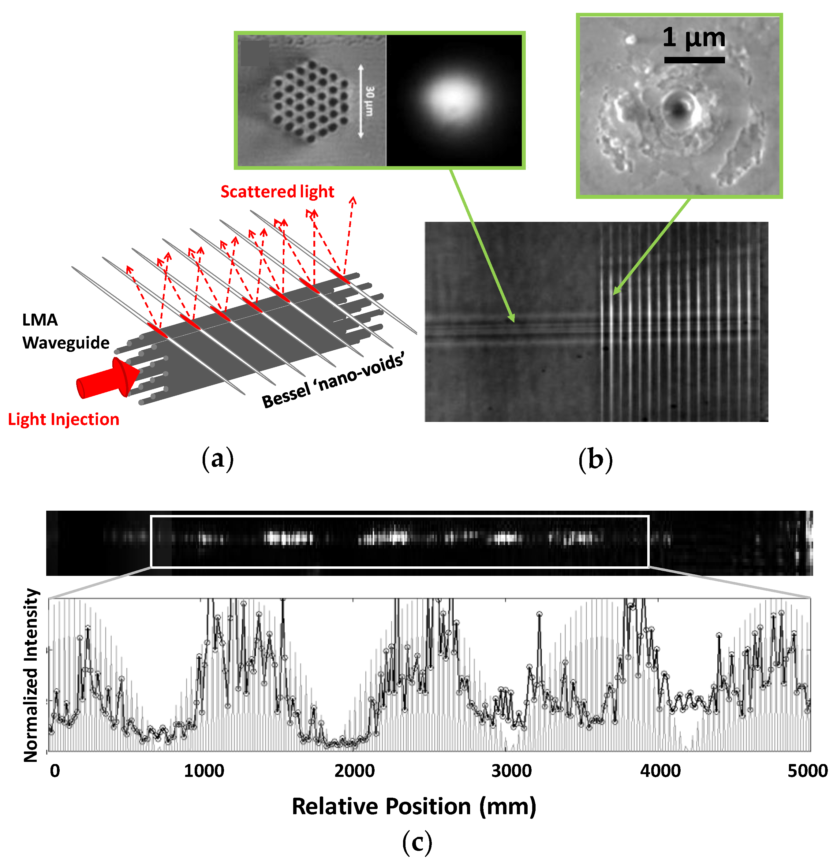
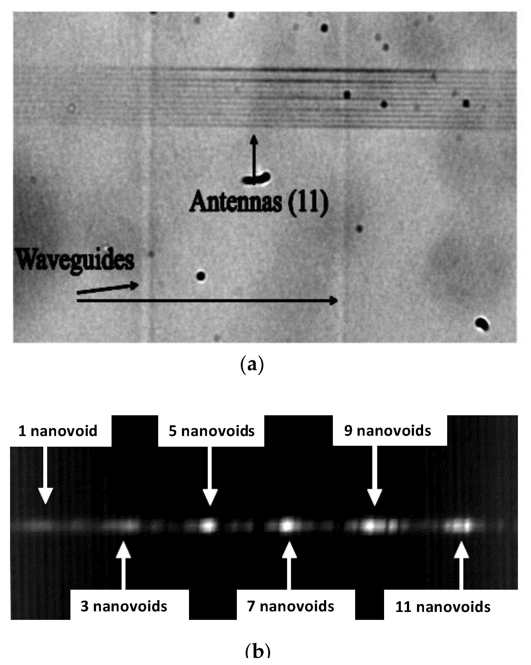
6.2. “Antennas” Geometry

One of the main problems of the 3D SWIFTS configuration presented above is that the waveguides being buried inside the material, and the signal radiated by each Bessel nanostructure having a wide angular distribution, gives crosstalk problems between pixels of a CCD positioned directly on the sample surface and used to detect the radiated signal. To overcome this problem, an implementation of multiple diffraction elongated Bessel nano-voids for each sampling position is proposed instead of a single nano-void, as a possible solution to improve the directivity of the information scattered towards the detector. Therefore, a single scattering center is formed by a grating containing several very close Bessel structures (see Figure 10a). Its efficiency is demonstrated by both simulated and measured far-field radiative patterns [84] exhibiting a promising method to be used for future integrated IR-SWIFTS. The implementation of the antenna geometry allows therefore for improving the resolution of embedded spectrometers in the IR domain, realized by DLW. In the experimental characterization, the sample was observed through a microscope objective from above in order to collect the signal radiated by different antennas (several groups with a different number of Bessel nanostructures), having therefore an overview of the radiated pattern. In the study the considered number of nanostructures per sampling group were 1, 3, 5, 7, 9, 11, as indicated in Figure 10b. Although the best result is theoretically expected with 11 nanostructures, this was not the case for the experimental observation. The reason is that the error made in positioning the nanostructure has a larger influence for a higher number of nanostructures, resulting in ghost signals and decreasing the contrast. Experimentally, the best compromise was found with a group of five nanostructures [84], as can be seen in Figure 10b.

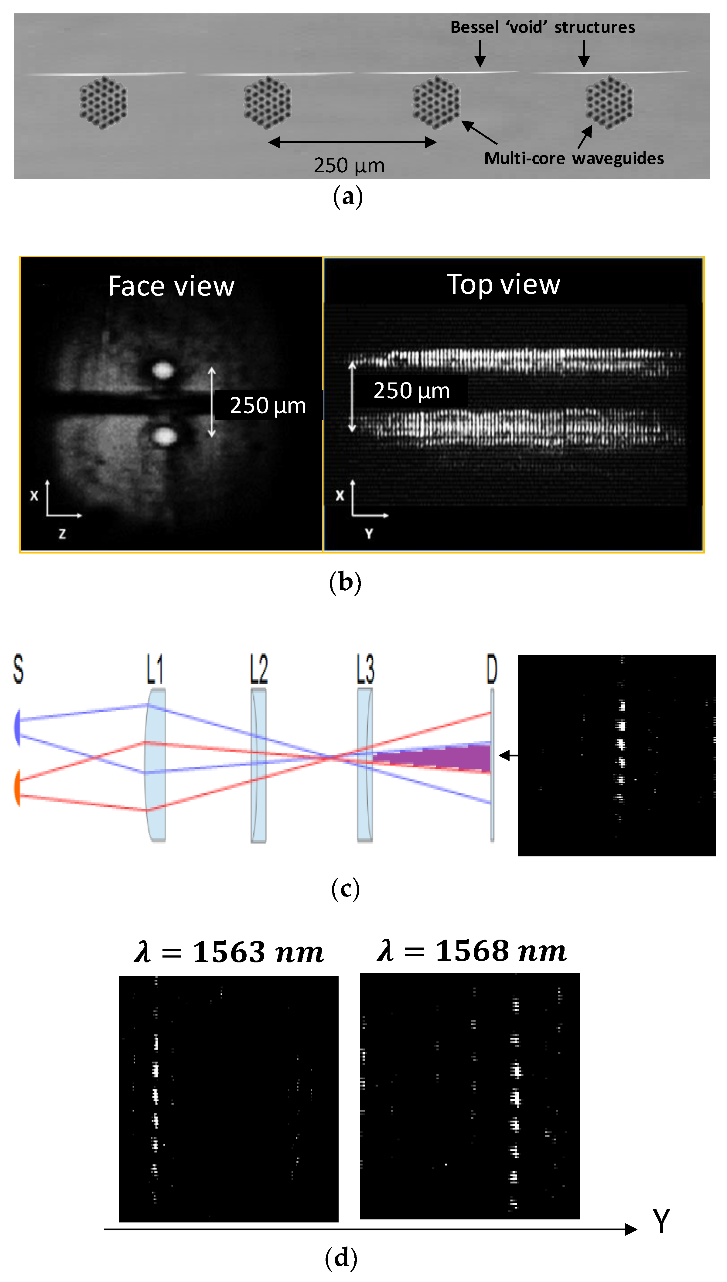
6.3. Demonstration of an Integrated Spectro-Interferometer in GLS

An alternative approach to the SWIFTS concept is obtained by extracting the optical signal confined in the waveguide, scattered by the periodic nano-voids, by using a relay optical system, which generates the spectrum at its Fourier plane, where the detector is placed [85]. Chromatic aberrations due to the imaging system can be limited by using a-focal optics. Although the spectral resolution is less than in the case of SWIFTS configuration, the most important advantage of this device is its flexibility, given by the possibility to image several parallel waveguides and therefore obtain the spectrum of different sources simultaneously, as each waveguide represents one input source (a telescope) and is re-imaged on the detector. Within a defocused configuration, this method allows overlapping the different inputs (in this work, up to four channels or “telescopes”) using a non-redundant configuration, which can be used in spectro-interferometry applications. The spectrometer prototype was made by a set of four LMA channel waveguides aligned in a plane, with a center-to-center separation of 250 µm. Each waveguide was obtained by using 37 honeycomb multicore array configuration (Figure 11a). Perpendicularly photo-written periodic Bessel scattering nano-voids, separated by 30 µm, were used for extracting the signal. As for the SWIFTS configuration, also in this case the characteristic section of each Bessel nanovoids is below 500 nm and the axial length is about 150 µm.
In similar works [85], within a 2D planar geometry, a large waveguide (4 mm wide) is used, so that the collimated beam sampled by a large scattering center is focused in a single spot. However, such a large waveguide implies multimode behavior, resulting in overlapping between different modes with different wavelengths. On the contrary, using a single mode, narrow waveguide, one can avoid high order diffraction modes, but the radiation pattern becomes angularly large. Besides, as demonstrated by full vectorial calculations, surface periodic nanostructures are not the most efficient approach in planar geometry, as most of the flux is radiated towards the substrate [82]. In the present 3D configuration, as the sampling centers are buried in the material, a symmetric radiation pattern is expected, resulting in a more efficient flux extraction towards the sample surface. In order to efficiently recover the flux, and discriminate eventually different order modes, a simple optical set-up has been developed using a cylindrical lens for collecting the wide-angle flux and focus different wavelengths at different pixels of the CCD, and a second optical stage to reduce aberrations, disperse laterally diffraction modes and avoid overlapping. The optical set-up is shown in Figure 11c and described in detail in ref. [10].
An IR tunable laser (Yenista), which can be tuned from 1500 to 1620 nm, was used to inject the waveguides. Two adjacent waveguides were simultaneously injected. A front view image of the two waveguide outputs, detected by an FLIR camera, is shown on the left of Figure 11b. The image of the light scattered by the periodic Bessel nano-voids from above, obtained using a simple microscope objective, is shown on the right of Figure 11b. The extracted signal is then detected on a Goodrich near IR camera placed on the image plane of the imaging system. When two contiguous channel waveguides are injected simultaneously, the spectrum in the horizontal direction for each input channel is obtained. If the imaging optical system is defocused in order to obtain overlapping on the CCD of signals diffracted from the two waveguides, typical Young interference fringes between the two sources appear in the vertical direction (X), as shown in Figure 11c. In this case, interference fringes are obtained vertically in a band that will move horizontally as the wavelength of the source is scanned (see Figure 11d), allowing the system working as a spectrometer and an interferometer at the same time. Note that in principle, it could be possible to distinguish between the periods of the Young fringes at different wavelengths, although this is experimentally difficult to obtain, due to technical limitations. However, the Young fringes could be efficiently discriminated when different pairs of waveguides were injected. This confirms that one can use the vertical dimension for studying interference between sources (for example, two different collecting telescopes), whilst using the horizontal dimension for spectral dispersion. A measurement of the whole set-up spectral resolution is given in ref. [10]. It has been found that, at best, an experimental resolution of 0.4 nm could be obtained despite a theoretical resolution of 0.1 nm being expected. The experimental characterization shows that the main limiting factor is the accuracy of the sampling centers period. It can be estimated that, in the present experimental conditions, any error in the positioning of the scattering nano-voids higher than 10 nm will imply flux leakage to adjacent pixels of the CCD, giving a degradation of the spectral resolution. Reaching this precision is expected to be a hard task for direct laser writing techniques. However, as a perspective, technical limitations due to mechanical deficiencies can be overcome by advanced laser synchronization methods and stage performances.

7. Photoinscription of 3D Nonlinear Optical Functions in Bulk ChG Glasses

Designing bulk 3D optical functions with additional Kerr nonlinearity becomes possible in ChGs, due to their high nonlinear index, enabling the development of all-optical signal processing concepts based on the excitation of spatial and temporal solitons at relatively low peak powers [53,86]. In this context, evanescently coupled two-dimensional waveguide arrays with a third-order nonlinear response have been proposed for light manipulation due to the strong sensitivity to injected power and subsequent discrete coupling [87,88,89,90]. A good example in this sense is represented by the function of a passive saturable absorber with a variable modulation depth [91] relying on discrete nonlinear localization of light in arrays of coupled waveguides [87]. The nonlinear waveguide arrays geometry is particularly interesting as the fabrication procedure can be extended to 3D embedded designs in ChG glasses using the ultrafast DLW technique. The design of such an optical device in bulk glasses implies the photo-inscription of Type I waveguide in longitudinal configuration and in a centered hexagonal arrangement, where the maximum transfer from the central to the side waveguides can reach up to 86% [92], controllable via the length and the index contrast of the surrounding waveguides. In the present case, the Type I central waveguide has a length of 9.1 mm, with the surrounding hexagon at a length of 2.4 mm. Details about the irradiation conditions can be found in ref. [93]. Type I positive index waveguides with typical index contrasts in the range of 10−4−10−3 were generated. A summary of the optical performance of the device, with its conceptual design, is shown in Figure 12a. Upon core injection with ps-long pulsed laser at 800 nm, the collective optical response of the waveguide array shows a strong intensity dependence, with the low-power propagating field being redistributed between the central core and the surrounding waveguides due to evanescent coupling, and high-power favoring decoupling and core propagation. Figure 12b indicates the measured low-power (around 0.2 kW) repartition of energy in the structure, with a minimal amount localized in the core. Increasing the intensity, the Kerr contribution increases the effective index of the central waveguide and the light becomes self-localized (Figure 12c), achieving more than 90% transmission in a stable manner. The power-dependent field propagation in the core suggests its potential as a saturable absorber. We noted that femtosecond injection leads to output transmission fluctuations, due to pulse spatial and temporal nonlinear distortions during propagation in the array. The spatiotemporal propagation of the pulses in the micro-structured GLS sample has been modeled by means of a discrete–continuous version of the UMEs [86], as described in detail in ref. [93]. The results for simulation concerning the picosecond input case are given in Figure 12d. This presents the fluence profile at the output of the saturable absorber for two levels of input pulse intensity. The modal profiles are comparable to the experimental profiles shown in Figure 12b,c, which were taken under similar input conditions. The overall transmission response of the saturable absorber (with respect to the performance of a single waveguide) is summarized in Figure 12e, which displays the experimental transmission data in the central core as a function of the estimated peak intensity of the injected pulse. The analogous results of the simulation are shown in the same graph (calculated assuming all the energy of the pulse is coupled in the waveguide), indicating good agreement between experiment and theory.

8. Conclusions

In conclusion, we have explored ultrafast photo-inscription concepts for designing laser-written waveguides in sulfur-based chalcogenide glasses, which are compatible with light transport in the infrared and mid-infrared spectral domains. They emphasize a correlation between irradiation design and material engineering. In particular, we demonstrated that the focal slit-shaping technique and evanescently-coupled and structured multicore waveguides are efficient solutions for large-mode-area guiding in the infrared ranges. Concerning the study of the response to ultrafast lasers, we showed how Ge-doping an As-S chalcogenide structure increases the structural flexibility of S-based chalcogenide glasses, allowing for a larger processing window of Type I positive index changes, via photo-induced local contraction. Equally, we showed how the thermal history of the sample can influence its structural flexibility, a short annealing time under Tg corresponding to a reduced packaging, allowing for a more efficient response. Equally, we put in evidence a new mechanism that increases the nonlinear photosensitivity of Ge-As-S chalcogenides after short annealing cycles under Tg, but it does not affect the structural flexibility. Depending on the slope of the heating ramp, this new mechanism is non-entropic and it is in competition with the entropic physical ageing of the glass structure (relaxation of the enthalpy), revealed for much longer annealing periods. Time-resolved studies of the glass response have been also presented in Ge15As15S70 and GLS glasses. We observed the electronic and thermomechanical relaxation dynamics over the entire evolution cycle for laser modifications corresponding to local densification and nano-void structure formation using Bessel beams. A multitude of physical processes were dynamically followed, from the initial plasma phase down to thermal and mechanical dissipation of energy. The observation of the excitation-relaxation cycles suggests low density generated plasmas in the case of Type I changes, and higher, but sub-critical excitation densities and onset of thermomechanical phenomena for Type II modifications. The strong interaction regime producing Type II index changes can result in material rupture and void formation, probably related to a slow liquid cavitation process, as in the case of fused silica. This ensures equally the nanoscale dimension of the void. The combination of micro and nanoscale capability are key to control light transport and to access the information contained in the optical fields. From an applicative point of view, we demonstrated how using multiscale laser processing, from micron-sized large-mode-area waveguides traces to nanoscale one-dimensional Bessel scatterers, it is possible to obtain compact high spectral and spatial resolution spectrometer and interferometer designs, embedded in the bulk of chalcogenide glasses and working in the infrared domain. By direct laser photo-inscription, it is possible to design the modal characteristics, such as waveguide refractive index, as well as the length of the diffraction nanovoids grating, so that the spectral resolution and the spectral bandwidth can be easily tuned, giving to these photowritten embedded photonic prototype a very high flexibility. The obtained results, although preliminary and to be optimized, are encouraging for lightweight applications, such as drone and cubesat interferometry projects, where we expect this type of compact spectro-interferometers to be a good tradeoff between performances and fabrication time and cost. Finally, we demonstrated how by exploiting the high nonlinearity of chalcogenide glasses (GLS in the present case), nonlinear embedded optical functions can be also defined. In particular, we demonstrated a near-infrared saturable absorber 3D concept based on ultrafast laser-fabricated coupled waveguide arrays, suitable for infrared ultrashort laser pulses at a low, kilowatt threshold.

Funding

This research was funded by Agence Nationale de la Recherche (ANR) (ANR 2011 BS04010 NanoFlam, ANR 2011 BS09026 SmartLasir); Labex Manutech-SISE (ANR-10-LABX-0075), of the Université de Lyon, within the program Investissements d’Avenir (ANR-11-IDEX-0007) operated by ANR. Photonic applications were co-funded by Action Spécifique Haute Résolution Angulaire (ASHRA) from CNRS and Labex FOCUS ANR-11-LABX-0013.

Institutional Review Board Statement

Not applicable.

Informed Consent Statement

Not applicable.

Acknowledgments

Authors are infinitely grateful to Manoj Bhuyan, Praveen Kumar Velpula, Guodong Zhang, Madhura Somayaji, Virginie Nazabal, and Stefano Minardi for their precious contribution to the studies presented in this review.

Conflicts of Interest

The authors declare no conflict of interest. The funders had no role in the design of the study; in the collection, analyses, or interpretation of data; in the writing of the manuscript, or in the decision to publish the results.

References

  1. Davis, K.M.; Miura, K.; Sugimoto, N.; Hirao, K. Writing waveguides in glass with a femtosecond laser. Opt. Lett. 1996, 21, 1729–1731. [Google Scholar] [CrossRef] [PubMed]
  2. Itoh, K.; Watanabe, W.; Nolte, S.; Schaffer, C. Ultrafast processes for bulk modification of transparent materials. MRS Bull. 2006, 31, 620–625. [Google Scholar] [CrossRef] [Green Version]
  3. Nolte, S.; Will, M.; Burghoff, J.; Tünnermann, A. Femtosecond waveguide writing: A new avenue to three-dimensional integrated optics. Appl. Phys. A Mater. Sci. Process. 2003, 77, 109–111. [Google Scholar] [CrossRef]
  4. Pacchioni, G.; Skuja, L.; Griscom, D.L. Defects in SiO2 and Related Dielectrics: Science and Technology; Kluwer Academic Publishers: Dordrecht, The Netherlands, 2000. [Google Scholar]
  5. Mishchik, K.; D’Amico, C.; Velpula, P.K.; Mauclair, C.; Ouerdane, Y.; Boukenter, A.; Stoian, R. Ultrafast laser-induced electronic and structural modifications in bulk fused silica. J. Appl. Phys. 2013, 114, 133502. [Google Scholar] [CrossRef]
  6. Masselin, P.; Le Coq, D.; Cuisset, A.; Bychkov, E. Spatially resolved Raman analysis of laser induced refractive index variation in chalcogenide glass. Opt. Mater. Express 2012, 2, 1768–1775. [Google Scholar] [CrossRef]
  7. Cheng, G.; D’Amico, C.; Liu, X.; Stoian, R. Large mode area waveguides with polarization functions by volume ultrafast laser photoinscription of fused silica. Opt. Lett. 2013, 38, 1924–1926. [Google Scholar] [CrossRef]
  8. Thomson, R.R.; Birks, T.A.; Leon-Saval, S.G.; Kar, A.K.; Bland-Hawthorn, J. Ultrafast laser inscription of an integrated photonic lantern. Opt. Express 2011, 19, 5698–5705. [Google Scholar] [CrossRef] [PubMed] [Green Version]
  9. D’Amico, C.; Cheng, G.; Mauclair, C.; Troles, J.; Calvez, L.; Nazabal, V.; Caillaud, C.; Martin, G.; Arezki, B.; LeCoarer, E.; et al. Large-mode-area infrared guiding in ultrafast laser written waveguides in sulfur-based chalcogenide glasses. Opt. Express 2014, 22, 13091–14001. [Google Scholar] [CrossRef] [PubMed]
  10. Martin, G.; Bhuyan, M.; Troles, J.; D’Amico, C.; Stoian, R.; Le Coarer, E. Near infrared spectro-interferometer using femtosecond laser written GLS embedded waveguides and nano-scatterers. Opt. Express 2017, 25, 8386–8397. [Google Scholar] [CrossRef]
  11. Cvetojevic, N.; Jovanovic, N.; Gross, S.; Norris, B.; Spaleniak, I.; Schwab, C.; Withford, M.J.; Ireland, M.; Tuthill, P.; Guyon, O.; et al. Modal noise in an integrated photonic lantern fed diffraction-limited spectrograph. Opt. Express 2017, 25, 25546–25565. [Google Scholar] [CrossRef] [Green Version]
  12. Watanabe, W.; Kuroda, D.; Itoh, K.; Nishii, J. Fabrication of Fresnel zone plate embedded in silica glass by femtosecond laser pulses. Opt. Express 2002, 10, 978–983. [Google Scholar] [CrossRef]
  13. Monat, C.; Domachuk, P.; Eggleton, B.J. Integrated optofluidics: A new river of light. Nat. Photonics 2007, 1, 106–114. [Google Scholar] [CrossRef]
  14. Marshall, G.D.; Dekker, P.; Ams, M.; Piper, J.A.; Withford, M.J. Directly written monolithic waveguide laser incorporating a distributed feedback waveguide-Bragg grating. Opt. Lett. 2008, 33, 956–958. [Google Scholar] [CrossRef]
  15. Sansoni, L.; Sciarrino, F.; Vallone, G.; Mataloni, P.; Crespi, A.; Ramponi, R.; Osellame, R. Polarization Entangled State Measurement on a Chip. Phys. Rev. Lett. 2010, 105, 200503. [Google Scholar] [CrossRef] [PubMed] [Green Version]
  16. Caulier, O.; LeCoq, D.; Bychkov, E.; Masselin, P. Direct laser writing of buried waveguide in As2S3 glass using a helical sample translation. Opt. Lett. 2013, 38, 4212–4215. [Google Scholar] [CrossRef] [PubMed]
  17. Bland-Hawthorn, J.; Kern, P. Astrophotonics: A new era for astronomical instruments. Opt. Express 2009, 17, 1880–1884. [Google Scholar] [CrossRef] [PubMed] [Green Version]
  18. Ta’eed, V.G.; Baker, N.J.; Fu, L.; Finsterbusch, K.; Lamont, M.R.E.; Moss, D.J.; Nguyen, H.C.; Eggleton, B.J.; Choi, D.Y.; Madden, S.; et al. Ultrafast all-optical chalcogenide glass photonic circuits. Opt. Express 2007, 15, 9205–9221. [Google Scholar] [CrossRef] [PubMed]
  19. Thomson, R.R.; Kar, A.K.; Allington-Smith, J. Ultrafast laser inscription: An enabling technology for astrophotonics. Opt. Express 2009, 17, 1963–1969. [Google Scholar] [CrossRef] [Green Version]
  20. Jovanovic, N.; Tuthill, P.G.; Norris, B.; Gross, S.; Stewart, P.; Charles, N.; Lacour, S.; Ams, M.; Lawrence, J.S.; Lehmann, A.; et al. Starlight demonstration of the Dragonfly instrument: An integrated photonic pupil-remapping interferometer for high-contrast imaging. Mon. Not. R. Astron. Soc. 2012, 427, 806–815. [Google Scholar] [CrossRef] [Green Version]
  21. Cvetojevic, N.; Norris, B.R.M.; Gross, S.; Jovanovic, N.; Arriola, A.; Lacour, S.; Kotani, T.; Lawrence, J.S.; Withford, M.J.; Tuthill, P. Building hybridized 28-baseline pupil-remapping photonic interferometers for future high-resolution imaging. Appl. Opt. 2021, 60, D33–D42. [Google Scholar] [CrossRef]
  22. Eggleton, B.; Luther-Davies, B.; Richardson, K. Chalcogenide photonics. Nat. Photonics 2011, 5, 141–148. [Google Scholar] [CrossRef]
  23. Hu, J.; Meyer, J.; Richardson, K.; Shah, L. Feature issue introduction: Mid-IR photonic materials. Opt. Mater. Express 2013, 3, 1571–1575. [Google Scholar] [CrossRef]
  24. Sanghera, J.S.; Aggarwal, I.D. Active and passive chalcogenide glass optical fibers for IR applications: A review. J. Non Cryst. Solids 2008, 256–257, 462–467. [Google Scholar] [CrossRef]
  25. Gai, X.; Han, T.; Prasad, A.; Madden, S.; Choi, D.-Y.; Wang, R.; Bulla, D.; Luther-Davies, B. Progress in optical waveguides fabricated from chalcogenide glasses. Opt. Express 2010, 18, 26635–26646. [Google Scholar] [CrossRef]
  26. Labadie, L.; Martin, G.; Anheier, N.C.; Arezki, B.; Qiao, H.A.; Bernacki, B.; Kern, P. First fringes with an integrated-optics beam combiner at 10µm. A new step towards instrument miniaturization for mid-infrared interferometry. Astron. Astrophys. 2011, 531, A48–A54. [Google Scholar] [CrossRef] [Green Version]
  27. Vázquez, M.R.; Sotillo, B.; Rampini, S.; Bharadwaj, V.; Gholipour, B.; Fernández, P.; Ramponi, R.; Soci, C.; Eaton, S.M. Femtosecond laser inscription of nonlinear photonic circuits in Gallium Lanthanum Sulphide glass. J. Phys. Photonics 2019, 1, 015006. [Google Scholar] [CrossRef]
  28. Kanbara, H.; Fujiwara, S.; Tanaka, K.; Nasu, H.; Hirao, K. Third-order nonlinear optical properties of chalcogenide glasses. Appl. Phys. Lett. 1997, 70, 925–927. [Google Scholar] [CrossRef] [Green Version]
  29. Bindra, K.S.; Bookey, H.T.; Kar, A.K.; Wherrett, B.S.; Liu, X.; Jha, A. Nonlinear optical properties of chalcogenide glasses: Observation of multiphoton absorption. Appl. Phys. Lett. 2001, 9, 1939–1941. [Google Scholar] [CrossRef]
  30. Zakery, A.; Elliott, S. Optical properties and applications of chalcogenide glasses: A review. J. Non Cryst. Solids 2003, 330, 1–12. [Google Scholar] [CrossRef]
  31. Sanghera, J.S.; Florea, C.M.; Shaw, L.B.; Pureza, P.; Nguyen, V.Q.; Bashkansky, M.; Dutton, Z.; Aggarwal, I.D. Non-linear properties of chalcogenide glasses and fibers. J. Non Cryst. Solids 2008, 354, 462–467. [Google Scholar] [CrossRef]
  32. Eggleton, B.J. Chalcogenide photonics: Fabrication, devices and applications Introduction. Opt. Express 2010, 18, 26632–26634. [Google Scholar] [CrossRef]
  33. Hewak, D.W.; Brady, D.; Curry, R.J.; Elliott, G.; Huang, C.C.; Hughes, M.; Knight, K.; Mairaj, A.; Petrovich, M.N.; Simpson, R.E.; et al. Chalcogenide glasses for photonics device applications. In Photonic Glasses and Glass-Ceramics; Murugan, G.S., Ed.; Research Signpost: Thiruananthapuram, India, 2010; pp. 29–102. [Google Scholar]
  34. Masselin, P.; Bychkov, E.; Le Coq, D. Direct laser writing of a low-loss waveguide with independent control over the transverse dimension and the refractive index contrast between the core and the cladding. Opt. Lett. 2016, 41, 3507–3510. [Google Scholar] [CrossRef] [PubMed]
  35. Kaiser, A.; Rethfeld, B.; Vicanek, M.; Simon, G. Microscopic processes in dielectrics under irradiation by sub-picosecond laser pulses. Phys. Rev. B 2000, 61, 11437–11450. [Google Scholar] [CrossRef]
  36. Fernandez, T.T.; Haro-González, P.; Sotillo, B.; Hernandez, M.; Jaque, D.; Fernandez, P.; Domingo, C.; Siegel, J.; Solis, J. Ion migration assisted inscription of high refractive index contrast waveguides by femtosecond laser pulses in phosphate glass. Opt. Lett. 2013, 38, 5248–5250. [Google Scholar] [CrossRef] [Green Version]
  37. Liu, Y.; Shimizu, M.; Zhu, B.; Dai, Y.; Qian, B.; Qiu, J.; Shimotsuma, Y.; Miura, K.; Hirao, K. Micro modification of element distribution in glass using femtosecond laser irradiation. Opt. Lett. 2009, 34, 136–138. [Google Scholar] [CrossRef] [Green Version]
  38. Zoubir, A.; Rivero, C.; Grodsky, R.; Richardson, K.; Richardson, M.; Cardinal, T.; Couzi, M. Laser-induced defects in fused silica by femtosecond IR irradiation. Phys. Rev. B 2006, 73, 224117. [Google Scholar] [CrossRef] [Green Version]
  39. Eaton, S.M.; Zhang, H.; Herman, P.R.; Yoshino, F.; Shah, L.; Bovatsek, J.; Arain, A.Y. Heat accumulation effects in femtosecond laser-written waveguides with variable repetition rate. Opt. Express 2005, 19, 4716–4808. [Google Scholar] [CrossRef]
  40. Mermillod-Blondin, A.; Burakov, I.M.; Meshcheryakov, Y.P.; Bulgakova, N.M.; Audouard, E.; Rosenfeld, A.; Husakou, A.; Hertel, I.V.; Stoian, R. Flipping the sign of refractive index changes in ultrafast and temporally shaped laser-irradiated borosilicate crown optical glass at high repetition rates. Phys. Rev. B 2008, 77, 104205. [Google Scholar] [CrossRef]
  41. Couairon, A.; Sudrie, L.; Franco, M.; Prade, B.; Mysyrowicz, A. Filamentation and damage in fused silica induced by tightly focused femtosecond laser pulses. Phys. Rev. B 2005, 71, 125435. [Google Scholar] [CrossRef]
  42. Saliminia, A.; Nguyen, N.T.; Chin, S.L.; Vallée, R. The influence of self-focusing and filamentation on refractive index modifications in fused silica using intense femtosecond pulses. Opt. Commun. 2004, 241, 529–538. [Google Scholar] [CrossRef]
  43. Burakov, I.M.; Bulgakova, N.M.; Stoian, R.; Mermillod-Blondin, A.; Audouard, E.; Rosenfeld, A.; Husakou, A.; Hertel, I.V. Spatial distribution of refractive index variations induced in bulk fused silica by single ultrashort and short laser pulses. J. Appl. Phys. 2007, 101, 043506. [Google Scholar] [CrossRef]
  44. Stoian, R.; Wollenhaupt, M.; Baumert, T.; Hertel, I.V. Pulse shaping in laser material processing. In Laser Precision Microfabrication; Sugioka, K., Meunier, M., Pique, A., Eds.; Springer Series in Optical Sciences; Springer: Heidelberg, Germany, 2010; Volume 135, p. 121. [Google Scholar]
  45. Stoian, R. Spatio-temporal effects in laser photoinscription of embedded waveguides. In Femtosecond Laser Machining; Osellame, R., Cerullo, G., Ramponi, R., Eds.; Springer Topics in Applied Physics; Springer: Berlin/Heidelberg, Germany, 2010; Volume 123, p. 67. [Google Scholar]
  46. Stoian, R.; Colombier, J.P.; Mauclair, C.; Bhuyan, M.K.; Velpula, P.K.; Srisungsitthisunti, P. Spatial and temporal laser pulse design for material processing on ultrafast scales. Appl. Phys. A Mater. Sci. Process. 2013, 114, 119–127. [Google Scholar] [CrossRef]
  47. Cheng, Y.; Sugioka, K.; Midorikawa, K.; Masuda, M.; Toyoda, K.; Kawachi, M.; Shihoyama, K. Control of the cross-sectional shape of a hollow microchannel embedded in photo-structurable glass by use of a femtosecond laser. Opt. Lett. 2003, 28, 55–57. [Google Scholar] [CrossRef]
  48. Osellame, R.; Taccheo, S.; Marangoni, M.; Ramponi, R.; Laporta, P.; Polli, D.; De Silvestri, S.; Cerullo, G. Femtosecond writing of active optical waveguides with astigmatically shaped beams. J. Opt. Soc. Am. B 2003, 20, 1559–1567. [Google Scholar] [CrossRef] [Green Version]
  49. Bhuyan, M.K.; Velpula, P.K.; Colombier, J.P.; Olivier, T.; Faure, N.; Stoian, R. Single-shot high aspect ratio bulk nanostructuring of fused silica using chirp-controlled ultrafast laser Bessel beams. Appl. Phys. Lett. 2014, 104, 021107. [Google Scholar] [CrossRef]
  50. del Hoyo, J.; de la Cruz, A.R.; Grace, E.; Ferrer, A.; Siegel, J.; Pasquazi, A.; Assanto, G.; Solis, J. Rapid assessment of nonlinear optical propagation effects in dielectrics. Sci. Rep. 2014, 5, 07650. [Google Scholar] [CrossRef] [PubMed] [Green Version]
  51. Diez-Blanco, V.; Siegel, J.; Solis, J. Femtosecond laser writing of optical waveguides with controllable core size in high refractive index glass. Appl. Phys. A Mater. Sci. Process. 2007, 88, 239–242. [Google Scholar] [CrossRef] [Green Version]
  52. McMillen, B.; Zhang, B.; Chen, K.P.; Benayas, A.; Jaque, D. Ultrafast laser fabrication of low-loss waveguides in chalcogenide glass with 0.65 dB/cm loss. Opt. Lett. 2012, 37, 1418–1420. [Google Scholar] [CrossRef] [Green Version]
  53. Keil, R.; Heinrich, M.; Dreisow, F.; Pertsch, T.; Tünnermann, A.; Nolte, S.; Christodoulides, D.N.; Szameit, A. All-optical routing and switching for three-dimensional photonic circuitry. Sci. Rep. 2011, 1, 94. [Google Scholar] [CrossRef] [PubMed] [Green Version]
  54. Minardi, S.; Dreisow, F.; Grüfe, M.; Nolte, S.; Pertsch, T. Three-dimensional photonic component for multichannel coherence measurements. Opt. Lett. 2012, 37, 3030–3130. [Google Scholar] [CrossRef]
  55. Crespi, A.; Osellame, R.; Ramponi, R.; Brod, D.J.; Galvao, E.F.; Spagnolo, N.; Vitelli, C.; Maiorino, E.; Mataloni, P.; Sciarrino, F. Integrated multimode interferometers with arbitrary designs for photonic boson sampling. Nat. Photonics 2013, 7, 545–549. [Google Scholar] [CrossRef]
  56. Vogel, M.M.; Abdou-Ahmed, M.; Voss, A.; Graf, T. Very-large-mode-area single- mode multicore fiber. Opt. Lett. 2009, 34, 2876–2878. [Google Scholar] [CrossRef] [PubMed]
  57. Long, X.; Bai, J.; Zhao, W.; Stoian, R.; Hui, R.; Cheng, G. Stressed waveguides with tubular depressed-cladding inscribed in phosphate glasses by femtosecond hollow laser beams. Opt. Lett. 2012, 37, 3138–3140. [Google Scholar] [CrossRef] [PubMed] [Green Version]
  58. Tang, W.; Zhang, W.; Liu, X.; Liu, S.; Stoian, R.; Cheng, G. Tubular depressed cladding waveguide laser realized in Yb: YAG by direct inscription of femto- second laser. J. Opt. 2015, 17, 05803. [Google Scholar] [CrossRef]
  59. Liu, X.; Zhang, W.; Zhao, W.; Stoian, R.; Cheng, G. Expanded-core waveguides written by femtosecond laser irradiation in bulk optical glasses. Opt. Express 2014, 22, 28771–28782. [Google Scholar] [CrossRef]
  60. Hisakumi, H.; Tanaka, K. Giant photoexpansion in As2S3 glass. Appl. Phys. Lett. 1994, 65, 2925. [Google Scholar] [CrossRef]
  61. Zarzycki, J. Glasses and the Vitreous State; Cambridge University Press: Cambridge, UK, 1991. [Google Scholar]
  62. Boesch, L.; Napolitano, A.; Macedo, P.B. Spectrum of Volume Relaxation Times in B2O3. J. Am. Ceram. Soc. 1970, 53, 148–153. [Google Scholar] [CrossRef]
  63. Macedo, P.; Napolitano, A. Effects of a distribution of volume relaxation times in the annealing of BSC glass. J. Res. Natl. Bur. Stand. 1967, 71, 231–238. [Google Scholar] [CrossRef] [PubMed]
  64. Calvez, L.; Yang, Z.; Lucas, P. Reversible giant photocontraction in chalcogenide glass. Opt. Express 2009, 17, 18581–18589. [Google Scholar] [CrossRef]
  65. D’Amico, C.; Caillaud, C.; Velpula, P.K.; Bhuyan, M.K.; Somayaji, M.; Colombier, J.-P.; Troles, J.; Calvez, L.; Nazabal, V.; Boukenter, A.; et al. Ultrafast laser-induced refractive index changes in Ge15As15S70 chalcogenide glass. Opt. Mater. Express 2016, 6, 1914–1928. [Google Scholar] [CrossRef]
  66. Gretzinger, T.; Fernandez, T.T.; Gross, S.; Arriola, A.; Withford, M.J. Boson band mapping: Revealing ultrafast laser induced structural modifications in chalcogenide glass. Opt. Lett. 2020, 45, 3369–3372. [Google Scholar] [CrossRef] [PubMed]
  67. Lucas, P.; King, E.A. Calorimetric characterization of photoinduced relaxation in GeSe9 glass. J. Appl. Phys. 2006, 100, 023502. [Google Scholar] [CrossRef]
  68. Caulier, O.; Le Coq, D.; Calvez, L.; Bychkov, E.; Masselin, P. Free carrier accumulation during direct laser writing in chalcogenide glass by light filamentation. Opt. Express 2011, 19, 20088–20096. [Google Scholar] [CrossRef]
  69. Hisakumi, H.; Tanaka, K. Optical microfabrication of chalcogenide glasses. Science 1995, 270, 974–975. [Google Scholar] [CrossRef]
  70. Somayaji, M.; D’Amico, C.; Wu, Y.; Troles, J.; Stoian, R. Influence of Thermal Annealing on Ultrafast Laser-Induced Local Densification in Bulk Sulfur-Based Chalcogenide Glasses. Phys. Status Solidi A 2019, 216, 1800568. [Google Scholar] [CrossRef]
  71. Smelser, C.W.; Mihailov, S.J.; Grobnic, D. Hydrogen loading for fiber grating writing with a femtosecond laser and a phase mask. Opt. Lett. 2004, 29, 2127–2129. [Google Scholar] [CrossRef]
  72. Royon, M.; Marin, E.; Girard, S.; Boukenter, A.; Ouerdane, Y.; Stoian, R. Photonics and Fiber Technology (ACOFT, BGPP, NP); OSA Paper BT3B.6; Technical Digest (Online): Sydney, Australia, 2016; Available online: https://www.osapublishing.org/abstract.cfm?uri=BGPP-2016-BT3B.6 (accessed on 11 May 2021).
  73. Royon, M.; Marin, E.; Girard, S.; Boukenter, A.; Ouerdane, Y.; Stoian, R. X-ray preconditioning for enhancing refractive index contrast in femtosecond laser photoinscription of embedded waveguides in pure silica. Opt. Mater. Express 2019, 9, 65–74. [Google Scholar] [CrossRef]
  74. Anderson, P.W.; Halperin, B.I.; Varma, C.M. Anomalous low-temperature thermal properties of glasses and spin glasses. Philos. Mag. 1972, 25, 1–9. [Google Scholar] [CrossRef]
  75. Phillips, W.A. Tunneling states in amorphous solids. J. Low Temp. Phys. 1972, 7, 351–360. [Google Scholar] [CrossRef]
  76. Galperin, Y.M.; Karpov, V.G.; Kozub, V.I. Localized states in glasses. Adv. Phys. 1989, 38, 669–737. [Google Scholar] [CrossRef]
  77. Durnin, J.; Miceli, J.J.; Eberly, J.H. Diffraction-free beams. Phys. Rev. Lett. 1987, 58, 1499–1501. [Google Scholar] [CrossRef] [PubMed]
  78. Velpula, P.K.; Bhuyan, M.K.; Courvoisier, F.; Zhang, H.; Colombier, J.P.; Stoian, R. Spatio-temporal dynamics in nondiffractive Bessel ultrafast laser nanoscale volume structuring. Laser Photonics Rev. 2016, 10, 230–244. [Google Scholar] [CrossRef]
  79. Mermillod-Blondin, A.; Mentzel, H.; Rosenfeld, A. Time-resolved microscopy with random lasers. Opt. Lett. 2013, 38, 4112–4115. [Google Scholar] [CrossRef]
  80. Somayaji, M.; Bhuyan, M.K.; Bourquard, F.; Velpula, P.K.; D’Amico, C.; Colombier, J.-P.; Stoian, R. Multiscale electronic and thermomechanical dynamics in ultrafast nanoscale laser structuring of bulk fused silica. Sci. Rep. 2020, 10, 15152. [Google Scholar] [CrossRef] [PubMed]
  81. Le Coarer, E.; Blaize, S.; Benech, P.; Stefanon, I.; Morand, A.; L’erondel, G.; Leblond, G. Wavelength-scale stationary-wave integrated Fourier-transform spectrometry. Nat. Photonics 2007, 1, 473–478. [Google Scholar] [CrossRef] [Green Version]
  82. Thomas, F.; Heidmann, S.; de Mengin, M.; Courjal, N.; Ulliac, G.; Morand, A.; Benech, P.; Le Coarer, E.; Martin, G. First Results in Near and Mid IR Lithium Niobate-Based Integrated Optics Interferometer Based on SWIFTS-Lippmann Concept. J. Light. Technol. 2014, 32, 4338–4344. [Google Scholar] [CrossRef]
  83. Bonneville, C.; Thomas, F.; de Mengin Poirier, M.; LeCoarer, E.; Benech, P.; Gonthiez, T.; Morand, A.; Coutant, O.; Morino, E.; Puget, R.; et al. SWIFTS: A groundbreaking integrated technology for high performances spectroscopy and optical sensors. In Proceedings of the SPIE MOEMS Photonics West, San Francisco, CA, USA, 2–7 February 2013. [Google Scholar]
  84. Bonduelle, M.; Martin, G.; Perez, I.H.; Morand, A.; D’Amico, C.; Stoian, R.; Zhang, G.; Cheng, G. Laser written 3D 3T spectro-interferometer: Study and optimisation of the laser-written nano-antenna. In Proceedings of the SPIE 11446, Optical and Infrared Interferometry and Imaging VII, 114462T, online, CA, USA, 13 December 2020. [Google Scholar]
  85. Avrutsky, I.; Chaganti, K.; Salakhutdinov, I.; Auner, G. Concept of a miniature optical spectrometer using integrated optical and micro optical components. Appl. Opt. 2006, 45, 7811–7817. [Google Scholar] [CrossRef] [PubMed] [Green Version]
  86. Büttner, T.F.S.; Hudson, D.D.; Mägi, E.C.; Bedoya, A.C.; Taunay, T.; Eggleton, B.J. Multicore, tapered optical fiber for nonlinear pulse reshaping and saturable absorption. Opt. Lett. 2012, 37, 2469–2471. [Google Scholar] [CrossRef] [PubMed]
  87. Bellec, M.; Panagiotopoulos, P.; Papazoglou, D.G.; Efremidis, N.K.; Couairon, A.; Tzortzakis, S. Observation and Optical Tailoring of Photonic Lattice Filaments. Phys. Rev. Lett. 2012, 109, 113905. [Google Scholar] [CrossRef]
  88. Szameit, A.; Blömer, D.; Burghoff, J.; Schreiber, T.; Pertsch, T.; Nolte, S.; Tünnermann, A.; Lederer, F. Discrete nonlinear localization in femtosecond laser written waveguides in fused silica. Opt. Express 2005, 13, 10552–10557. [Google Scholar] [CrossRef]
  89. Minardi, S.; Eilenberger, F.; Kartashov, Y.V.; Szameit, A.; Röpke, U.; Kobelke, J.; Schuster, K.; Bartelt, H.; Nolte, S.; Torner, L.; et al. Three-Dimensional Light Bullets in Arrays of Waveguides. Phys. Rev. Lett. 2010, 105, 263901. [Google Scholar] [CrossRef] [PubMed]
  90. Hudson, D.D.; Shish, K.; Schibli, T.R.; Kutz, J.N.; Christodoulides, D.N.; Morandotti, R.; Cundiff, S.T. Nonlinear femtosecond pulse reshaping in waveguide arrays. Opt. Lett. 2008, 33, 1440–1442. [Google Scholar] [CrossRef] [PubMed]
  91. Snyder, A.W. Coupled-Mode Theory for Optical Fibers. J. Opt. Soc. Am. 1972, 62, 1267–1277. [Google Scholar] [CrossRef]
  92. Zhao, H.; Major, A. Powerful 67 fs Kerr-lens mode-locked prismless Yb:KGW oscillator. Opt. Express 2013, 21, 31846–31851. [Google Scholar] [CrossRef] [PubMed] [Green Version]
  93. Minardi, S.; Cheng, G.; D’Amico, C.; Stoian, R. Low-power-threshold photonic saturable absorber in nonlinear chalcogenide glass. Opt. Lett. 2015, 40, 257–259. [Google Scholar] [CrossRef] [Green Version]
Figure 1. Spatio-temporal beam engineering methods using spatial and spectral phase modulation beam shaping in space and time domains. Examples of non-diffractive beams generation, parallel processing, beam slit-shaping, and time-envelope shaping are indicated.
Photonics 08 00211 g001
Figure 2. (a) Schematic of the beam slit-shaping technique applied to the transverse photo-inscription of buried waveguides; (b) Phase contrast images of the cross-section of a photo-inscribed trace in bulk Ge15As15S70 glass with a 30 mW laser pulse at 100 kHz (slit aperture 100 µm, focusing objectif with NA = 0.42). As can be seen, irradiation with femtosecond pulses determines extended damage around the core; (c) Irradiation results with elongated linearly chirped pulses, a durations of 20 ps can limit the collateral damage and create symmetric core traces; (d) The near-field image of the guided mode at the exit of the waveguide, at 800 nm, is given for the latter case.
Photonics 08 00211 g002
Figure 3. Multicore waveguiding results in Ge15As15S70 glass for ultrashort pulse irradiation; (a) Multicore cross-sectional profiles in PCM with increasing index contrast and respective guiding behavior at 800 nm. Visible mode confinement appears for higher index contrast. The transverse size is constant and equal to 30 µm; (b) Multicore cross-sectional profiles in PCM with increasing inter-trace spacing and corresponding mode behavior at 800 nm injection. In this case the index contrast is kept constant and the transverse dimensions from the left to the right are respectively 36, 42, and 48 µm; (c) Continuous large section structure obtained by overlapping traces in cross-section and in a side-view PCM perspective. A higher 800 nm mode LP21 is obtained; (d) Large section (100 µm) multicore (white light illumination) waveguide obtained with individual slit-shaped traces. Details about the experimental conditions are given in ref. [9].
Photonics 08 00211 g003
Figure 4. (a) MIR large band guiding in a multicore waveguide. The spectral dependencies of the laser-induced structures as a function of the index contrast is also shown. Two input powers at 2 and 6 mW are used with the same sample scan velocities of 0.1 mm/s, in order to obtain two different index contrasts. Higher contrast leads to better guiding in the large wavelength spectral domain; (b) Laser energy dose dependent spectral behavior of slit-shaped traces via two scan velocities (0.1 and 0.2 mm/s) at the same input power of 380 mW. Higher contrast leads to better guide transparency; however, overall performances lay below those of the multicore; (c) Multicore structure written in bulk Ge15As15S70 glass (10 mm length) at 2.4 mW, 100 kHz input laser conditions via a NA 0.5 aspherical lens at 0.5 mm/s scan speed. The inter-trace spacing is 5 µm, and the whole diameter 30 µm; (d) The corresponding single mode guided at 3.39 µm, detected via a FLIR camera [9]; (e) Finite element analysis for a guided mode at 3.39 µm in a multicore hexagonal structure with 5 µm spaced, 4 µm thick individual traces of NA = 0.08.
Photonics 08 00211 g004
Figure 5. Comparison of the refractive index change results (PCM) of the waveguide laser photo-inscription process in (a) As2S3 and (b) Ge15As15S70 glasses with the same laser parameters (2 mW (@100 kHz) and 160 fs duration) and for two different scanning speeds. The translation speeds of the samples are indicated on the images; (c) A quasi planar As-S molecular structure acquires a 3D connectivity (Ge-As-S) after doping with Ge, increasing its structural flexibility; (d,e) Comparison of the index change results (PCM) of the waveguide photo-inscription process in a pristine (top) and longtime re-annealed (bottom) Ge15As15S70 samples by 2 mW (@100 kHz) and 160 fs laser pulses, with two different scanning speeds. The translation speeds are indicated on the top; (f) Schematic of the thermal history of annealed chalcogenide glasses and its influence on the enthalpy of the microscopic glass structure.
Photonics 08 00211 g005
Figure 6. (a) Temperature vs. time behavior during the single short thermal cycle applied to ChG samples as measured at the center of the oven. The peak temperature Tmax and the glass transition temperature Tg corresponding to a specific sample are indicated in the text; (b) Variation of the laser-induced relative positive index contrast in Ge20As20S60 (pulse energy 30 nJ, pulse duration 150 fs, red stars), in Ge15As15S70 (pulse energy 40 nJ, pulse duration 150 fs, blue squares), and in GLS (pulse energy 400 nJ, pulse duration 150 fs, dark circles) as a function of the number of annealing cycles; (c) Enhancement of the ultrafast laser-induced index contrast in Ge20As20S60 during the two first annealing cycles (Tmax = 250 °C), for three values of the heating rate: 3 (dark arrows), 6 (blue arrows), and 20 °C/min (red arrows); (d) Type I index changes induced by a 30 nJ, 150 fs laser beam focused into the Ge20As20S60 sample before (dark circles) and after (red triangles) the first thermal annealing cycle (heating ramp: 20 °C/min, Tmax = 250 °C). The insets correspond to the cases of low laser exposure time (1 ms laser exposure time @ 100 kHz, inset bottom-left) and high laser exposure time (100 ms laser exposure time @ 100 kHz, inset on middle-right).
Photonics 08 00211 g006
Figure 7. (a) Time-resolved optical transmission microscopy imaging of the relaxation of the carrier plasma produced by a single-shot 1 µJ, 4ps Bessel laser pulse focused into Ge15As15S70; (b) Time-resolved imaging of plasma electron density with spatio-temporal excitation profiles; (c) Time-resolved phase contrast microscopy imaging; a pressure wave is clearly visible around 6 ns; (d) Averaged plasma electron density dynamics as function of the delay time between pump and probe; (e) Permanent Type II change produced in single-shot regime by a 1 µJ, 4 ps Bessel laser pulse focused into Ge15As15S70.
Photonics 08 00211 g007
Figure 8. (a) Time-resolved sequence of index contrast images corresponding to the appearance of a permanent positive index change (dark colors) induced by a single Bessel laser pulse. The evolution is monitored for a time domain ranging from about 1 ns to about 10 μs, with imaging delays given on the side of each snapshot. Input laser pulse parameters: 15 μJ and 2 ps. The laser beam arrives from the left; (b) Multiscale time-resolved sequence of index contrast images corresponding to the appearance of a void-like structure (light colors) induced by a single laser pulse. The evolution is monitored for a time domain ranging from about 1 ns to about 10 μs. Input laser pulse parameters: 20 μJ and 5.5 ps. The laser pulse comes from the left. The measurement is similar to the data reported in Ref. [80].
Photonics 08 00211 g008
Figure 9. (a) Schematic concept of LMA light transport and signal extraction optical functions, obtained by using multicore array waveguide concept (for guiding) and high aspect ratio Bessel nano-voids photo-written transversally to the waveguide (signal extraction by scattering); (b) Top-view of the prototype schematized in (a) fabricated in bulk GLS glass. The inset on the left shows the multicore cross-section of the fabricated LMA waveguide and the corresponding guided mode obtained by injecting the waveguide with a 1550 nm SLED. The inset on the right shows the cross-section of the single Bessel nano-void structure; (c) Sampling of the λ = 3.39 µm signal confined in the waveguide and extracted from the periodic Bessel nano-voids (input injection on the left, output interface on the right). Although the signal is under-sampled (discussion in the text), a stationary wave is clearly visible as formed in the waveguide by interference.
Photonics 08 00211 g009
Figure 10. (a) Photoinscription of a scattering element, made by a group of 11 Bessel nanovoids (this forms an antenna or mini-diffraction grating) inter-spaced by 3 µm; (b) Top-view of the signal scattered by groups of antennas with a different number of Bessel nanovoids.
Photonics 08 00211 g010
Figure 11. (a) Front-view schematic concept of the spectro-interferometer prototype photo-inscribed in bulk GLS, made by four LMA honeycomb multicore cross-section waveguides and transversally photowritten Bessel nanovoids; (b) Direct transmission on the FLIR camera, showing the two modes of two adjacent channel waveguides (left) and a top view of the signal extracted with the sampling centers and imaged on the Goodrich Camera using a simple microscope objective (right); (c) Left: optical set-up showing overlapping of the signal extracted from two adjacent waveguides as the triplet is defocused from the source plane. Right: corresponding Young fringes obtained on the detector, using a monochromatic source at 1560 nm, when two adjacent channel waveguides are simultaneously injected; (d) Image of the vertical interference fringes as they move on the detector (in the Y direction, with respect to Figure 11b) as the wavelength is tuned from 1563 to 1568 nm.
Photonics 08 00211 g011
Figure 12. (a) Conceptual design of the centered hexagonal array with a 9.1 mm length for the core guide and a 2.4 mm length for the surrounding hexagon. The inter-trace spacing is 13 μm; (b) Output mode in the case of low-power (0.2 kW) injection with a uniform spread of energy; (c) Output mode in the case of high-power (7 kW) injection with a core localization of light. The injected pulse duration (FWHM) is 3 ps; (d) Output mode snapshots resulting from the simulation of the propagation in the photonic saturable absorber of a λ = 800 nm positively chirped pulse of 3 ps, for an input pulse intensity of 2.5 GW/cm2 (top) and 25 GW/cm2 (bottom); (e) Intensity and power-dependent transmission in the hexagonal array. Experimental values (solid squares) and simulation data (open circles) are plotted. The x-error bars reflect the precision in evaluating the intensity via the accuracy of mode size estimations.
Photonics 08 00211 g012
Table 1. Refractive index (n), band-gap (Eg), nonlinear index (n2), glass transition temperature (Tg), thermal expansion coefficient (α), and Young modulus (Y) of the four chalcogenide samples considered in this study. The same parameters for fused silica are also given for comparison.
Glassn (@800 nm)Eg (eV)n2 (cm2/W)Tg (°C)α (K−1)Y (GPa)
As40S602.52.144.8 × 10−14 119221.6 × 10−616.5
Ge20As20S602.22.262.8 × 10−14 230522 × 10−6-
Ge15As15S702.22.392.8 × 10−14 220423 × 10−6-
GLS2.42.591 × 10−14 155510 × 10−659
Fused Silica1.4592.2 × 10−16 312000.5 × 10−671.7
1 See ref. [31]. 2 J. M. Harbold et al., IEEE Photonics Technology Letters 2020, 14, 822–824. 3 G. P. Agrawal, ed., Nonlinear fiber optics (3rd Edition, Academic Press, New York, NY, USA, 2001).
Publisher’s Note: MDPI stays neutral with regard to jurisdictional claims in published maps and institutional affiliations.

