1. Introduction
The swift growth in the capacity of communication networks has led to new services, such as mobile broadband for smart devices, social networking, cloud computing, and online streaming. To assist in this growth, the Ethernet standards have repeatedly been extended from 100 Gb/s to 400 Gb/s. In optical fiber communication systems, there is always a tradeoff between the transmission capacity and the transmission distance. The optical receiver is a major factor in extending the distance limited by the power transmitted from laser sources. In comparison to the conventional p-i-n photodiodes, high-sensitivity avalanche photodiodes (APDs) are a prerequisite for >25 Gbit/s operation across the telecommunication wavelength (1.31 to 1.55 μm), for the optical signal receivers over 40–80 km fibers in 100 and 400 Gbit/s ER-4 systems [
1]. Significant research has been done on possible alternative materials like silicon-germanium (Si/Ge) and the III-V compounds, such as InP, InGaAs, and InAlAs, for the fabrication of high-speed APDs for high data rate applications [
2]. However, the III-V based APDs have numerous advantages in terms of band engineering flexibility in which the materials can be lattice matched with the InP substrate during growth. Thus, high performance can be achieved by modifying the different stacked layers in the APD, varying the distinguishing features such as the bandgaps, electron, hole velocities, and diffusion coefficients. For example, by varying the thickness of the hybrid absorber layer, we can boost the speed of an APD for a given responsivity and vice versa. APDs with In
0.52Al
0.48As-based M-layers have attracted significant attention for 10 Gb/s and >25 Gb/s applications because the benefits of a large gain-bandwidth product, high temperature stability, and reasonably low dark current characteristics at the 1.31–1.55 μm wavelengths. In order to meet the requirements for high-speed transmission, a lot of effort has been made to improve the bandwidth and gain bandwidth product (GBP) of the device. For APDs >25 Gb/s operation, thin absorption (<1 μm) and M (<100 nm) layers with a small diameter of active mesa (<20 μm) are requisite [
3,
4,
5,
6], but this small diameter mesa leads to a degradation in the unit gain responsivity and offers less tolerance for optical alignment. Further improvement in the GBP, up to 140 GHz, has been reported using a 200 nm InAlAs avalanche layer [
7]. Nada et al., proposed an APD with a 100 nm avalanche layer, which could reach a GBP of 235 GHz with the diameter of 20 μm. Later, they further downscaled the multiplication layer thickness to 90 nm and achieved a GBP up to 270 GHz with the same 20 μm diameter [
5,
8,
9].
There are various factors limiting the speed, gain, and noise in the receiver performance in high-speed systems, for instance, the avalanche build-up time, which depends on the material and the thickness of the avalanche layer. Moreover, to further improve APD speed performance, very thin avalanche layers are generally required, to minimize the avalanche buildup time [
10]. However very thin avalanche layers are vulnerable to band-to-band tunneling currents, which increase exponentially with the electric field and add to the receiver noise. Thus, to avoid excessive tunneling currents, the thickness of the avalanche layer should be within the lower limits. In order to achieve a large GBP and low noise, it is necessary to adopt the appropriate thickness for the avalanche layer.
In this work, we demonstrate a novel design for In0.52Al0.48As based vertical illuminated APDs with dual M-layers. Separate absorption, grading, and multiplication (SAGM) structures with thin absorber and dual M-layer (Device A) versus thick absorber and dual M-layer (Device B) APDs are fabricated. The demonstrated APDs (Device A) are fabricated using a partially depleted p-type In0.53Ga0.47As absorbing layer and thin In0.52Al0.48As dual M-layers (60, 88 nm). We obtain a wide optical-to-electrical bandwidth 18 GHz and large gain bandwidth product (459 GHz). On the other hand, after further downscaling the active diameter, in its counterpart back-illuminated device (Device A′) exhibits a much wider O-E bandwidth of 25 GHz and a saturation current as high as >5 mA. whereas APD (Device B) design with thick absorber and dual M-layers, there is a relaxation in the trade-off between the avalanche gain and the bandwidth. An ultra-high gain bandwidth product (460 GHz), high responsivity (1 A/W) at the unit gain and a 3-dB bandwidth of 1.25 GHz with a responsivity as high as 33 A/W at 0.9 Vbr can be achieved using a device with a large optical window diameter (200 μm). It is worth noting that in either case (thin or thick multiplication layer), we obtain an ultra-high GBP of around 460 GHz. These promising results suggest that our proposed dual M-layer with thick absorber layer design can fundamentally overcome allow further downscaling of the M-layer and absorber layer to obtain a higher GBP, in order to meet the requirements of high-speed transmission. Nevertheless, such APDs with high GBP and high responsivity and a large optical window diameter (200 μm) can be fundamentally used for FMCW Lidar applications dealing with weak reflected signals received from the objects being tested.
2. Device Structure and Fabrication
Here, the static and dynamic performance of two types of devices (A and B) are studied in detail.
Figure 1a,b shows conceptual cross-sectional views of the demonstrated devices A and B, respectively, with their top-illuminated structure. Note that these figures are not drawn in scale. From top to bottom, the structure of both devices are composed of a p
+-In
0.53Ga
0.47As contact layer, p
+-In
0.52Al
0.48As window layer, graded/intrinsic In
0.53Ga
0.47As absorbing layer, two p-type In
0.52Al
0.48As charge layers, and N
+ In
0.52Al
0.48As/InP contact layers. For more detail about the epi-layer structure and the working principles of the demonstrated APDs (Device A), the interested reader can refer to our previous work [
11]. Two In
0.52Al
xGa
0.48-xAs graded bandgap layers are inserted at the interfaces between the absorber/window and absorber/multiplication layers. The thickness of each epi-layer is specified in detail in this figure.
The electric field distribution within the device was simulated using the Silvaco Technology Computer Aided Design (TCAD) tools (Semtech; 200 Flynn Road, Camarillo, CA 93012. Product: GN1085).
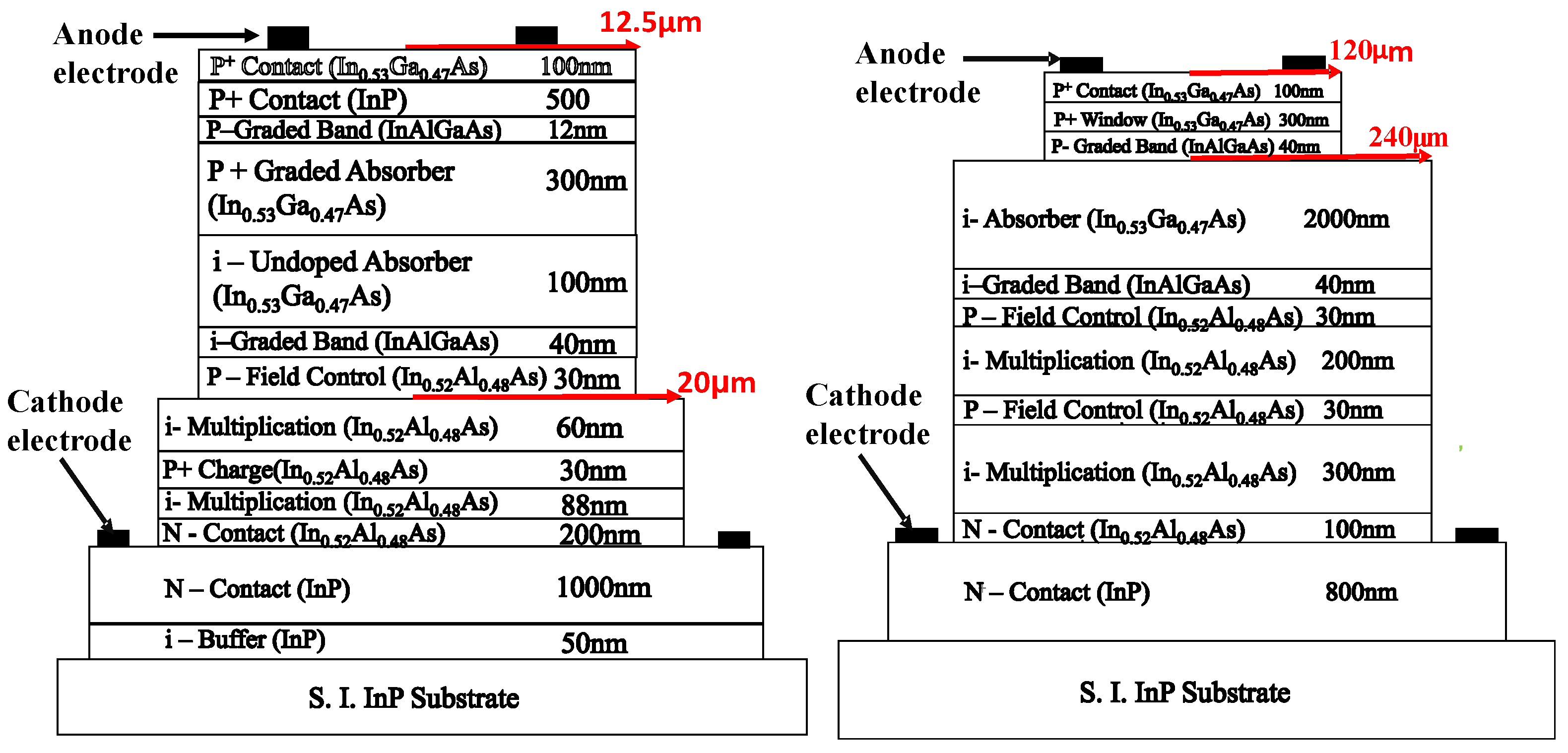
Figure 2a shows the calculated electric fields for Device B along the vertical direction at the punch-through (V
pt) and breakdown voltage (V
br). To obtain a stepped electric field profile for fabricated ADPs, the thick multiplication (M-) layer is divided into two partitions (148 nm divided into 60, 88 nm for Device A and 500 nm divided into 200 and 300 nm for Device B) with an additional charge control layer [
12]. APDs with dual M-layer are introduce stepped electric field profile, where the electrons will be energized by the first M-layer (from the top). However, the strength of the electric field is insufficient to trigger significant impact ionization, they transit to the second M-layer to initiate successive impact ionization. This design provides better localization of impact ionization than can be achieved in a uniformly thick M-layer, therefore it can reduce the delay time induced by the avalanche process in the APD.
Moreover, the stepped E-field may also reduce excess noise (k-factor) for the APD. Due to cascade avalanche process, a smaller avalanche delay time and an ultra-high GBP, compared to those of the traditional APD design can be expected. Similar working principles are realized for the impact-ionization-engineered (I
2E) APD structures [
13,
14], where the impact ionization process in the materials is localized with the narrowest bandgap in the M-layer, forming a hetero-junction with several different bandgap materials. In contrast to the I
2E structure, our M-layer acts as a homo-junction, but with several charge layers and different doping densities to localize the avalanche process in the region which has the highest E-field. As can be seen in
Figure 1a,b, the same triple mesa structure is adopted for both devices A and B, confining the E-field within the first mesa (active region) diameter of 25 μm and 240 μm, respectively. The first mesa is etched through the upper charge layer (field-control) and p-type window layer and stops at the 60 nm In
0.52Al
0.48As buffer layer and 2 μm thick In
0.53Ga
0.47As absorption layer in devices A and B, respectively. For detailed E-field distributions for our device structure please refer to our previous work [
12].
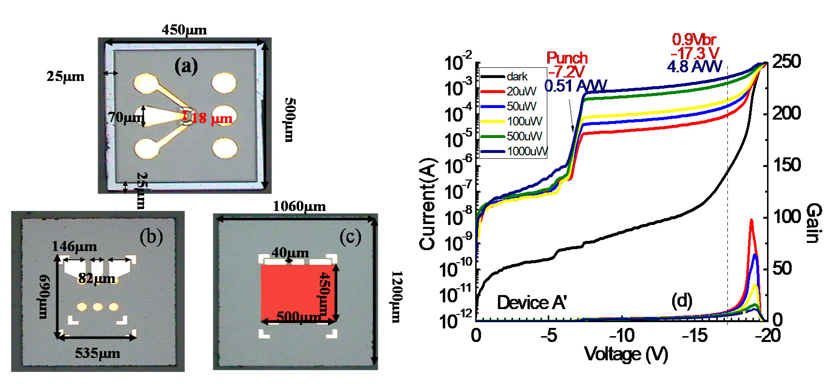
Figure 2b,c shows top-views of the fabricated devices with 25 μm and 240 μm mesa active diameters and corresponding optical windows of 12 μm and 200 μm for devices A and B.
3. Device Measurement Results
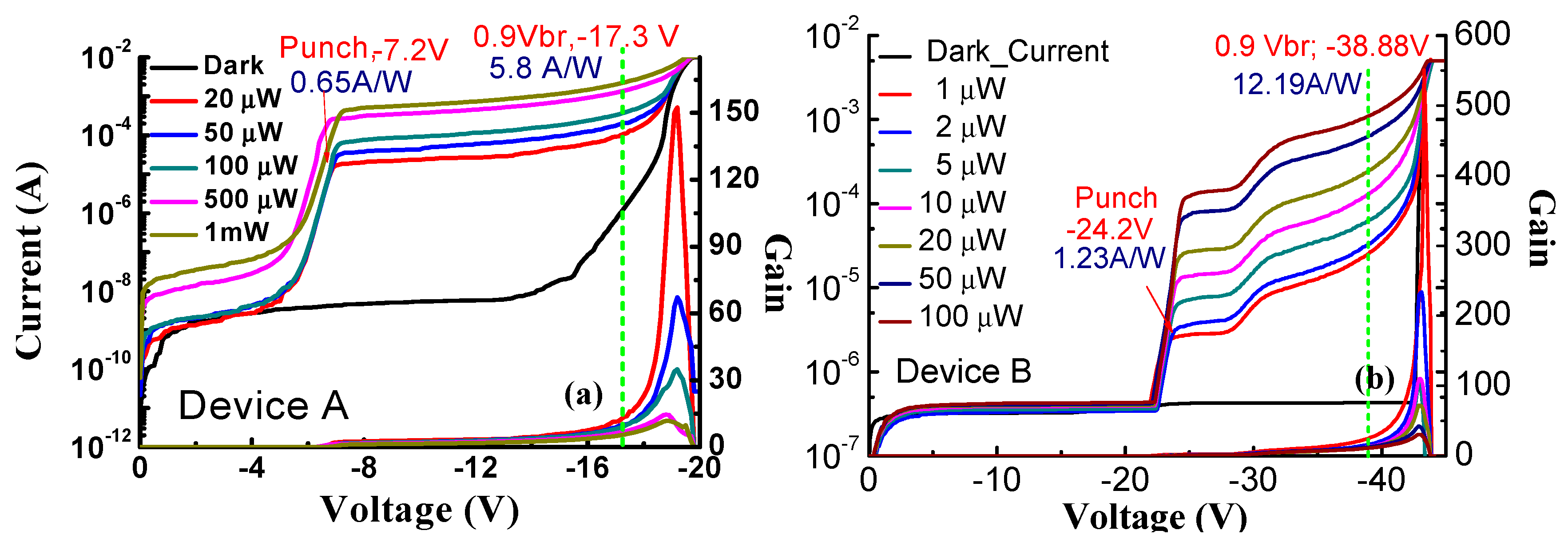
Figure 3a,b shows the measured bias-dependent dark current, photocurrent, and operation gain of the demonstrated APDs, subject to different optical pumping powers at optical wavelengths of 1.31 μm and 1.55 μm for devices A and B. As can be seen, the measured V
br and V
pt are around −19.5, −43 V and −7.2, −24.2 V for devices A and B. The smaller V
pt and V
br of Device A is attributed to the thinner absorber layer and thicker M-layer than that of Device B. Moreover, under 0.9 V
br operation, Device B has a higher responsivity than that of Device A which is due to the thicker absorption layer (2 versus 0.4 μm).
In addition, when the reverse bias is over V
pt, the photocurrent of Device B ramps up more quickly than that of Device A. This can be attributed to the precise control of charge layer doping in Device B which allows the E-field in its dual M-layers to be high enough to trigger the cascade avalanche process and generate a significant amount of multiplication gain. We assume a zero coupling loss and single-pass of injected light into the absorption layer of our device. The theoretical maximum unit gain responsivity of Device A (B) with a 0.4 (2.0) μm-thick In
0.53Ga
0.47As absorption layer, will be around 0.4 (1.0) A/W at the 1.31(1.55) μm wavelength. Here, the photo-absorption constant used for the In
0.53Ga
0.47As layer at wavelengths 1.31(1.55) μm are around 1.2 (0.8) μm
−1 [
15,
16]. The gain versus bias voltages under different optical pumping power (1 to 500 μW) are also provided in the figures for reference. As can be seen, there is a significant reduction in all the measured operation gain when the reverse bias voltage is over V
br due to the tremendous increase in the dark current, which occupies most of the measured total current (i.e., summation of photocurrent and dark current). In addition, we can clearly see that the maximum operation gain gradually decreases with increasing pumping power. This phenomenon can be explained by the space charge screening (SCS) effect induced by the photo-generation of holes in the undoped In
0.53Ga
0.47As absorption layer, which reduces the net E-field and multiplication gain in the M-layer [
11].
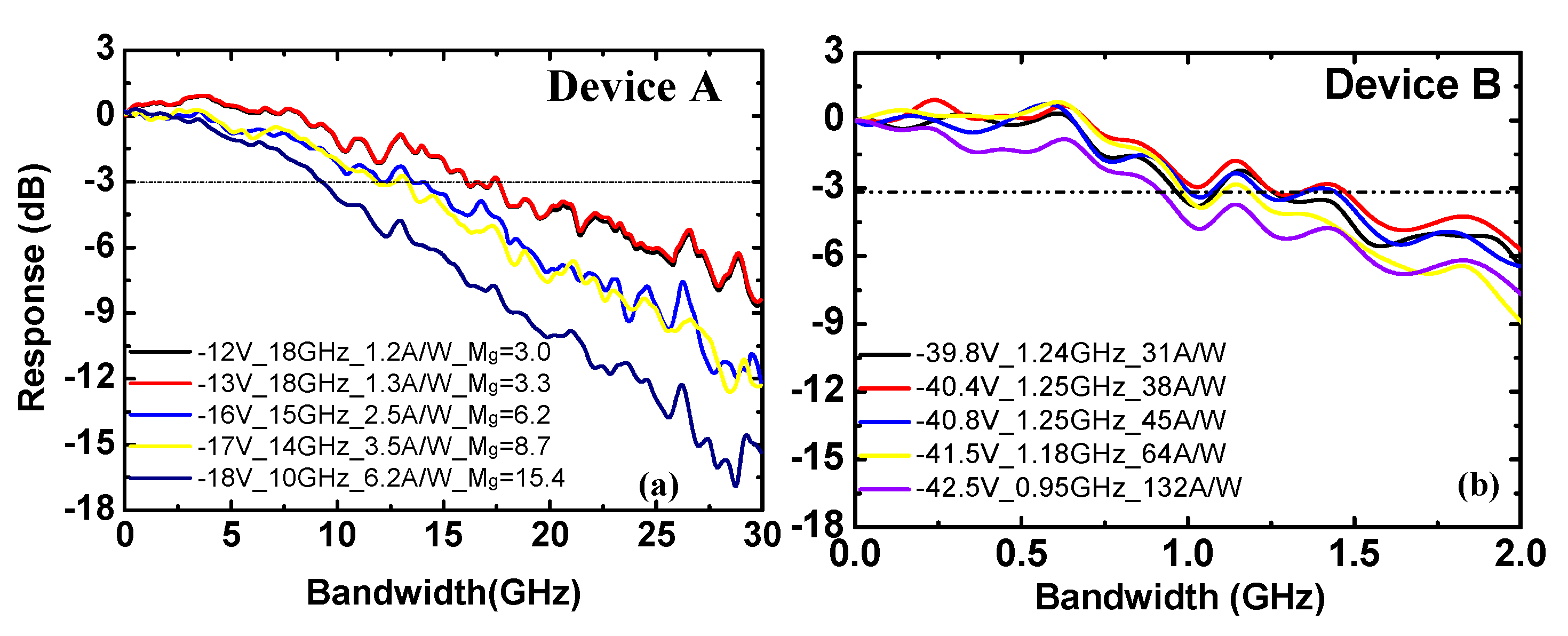
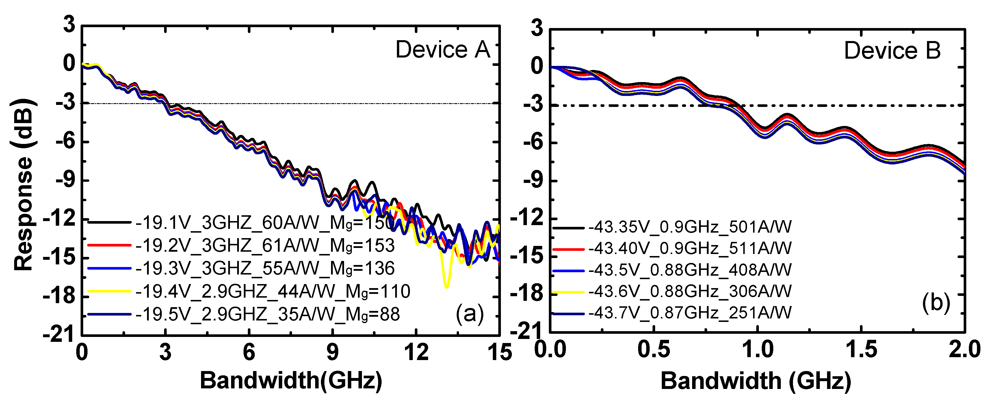
Figure 4a,b shows the 3-dB O-E bandwidth response, under a low optical pumping power of 50 (1) μW and operation gain at the 1.31(1.55) μm wavelength of Devices A and B, respectively. In both cases, under such a low optical pumping power, we can clearly see a gradual decrease in the measured O-E bandwidth with an increase of the reverse bias voltage (operation gain). The maximum 3-dB O-E bandwidths of Devices A and B are around 18 and 1.25 GHz, respectively. The degradation in the O-E bandwidth with the increase of operation gain is very common in APDs and can be attributed to the increase of the avalanche induced delay time with the gain.
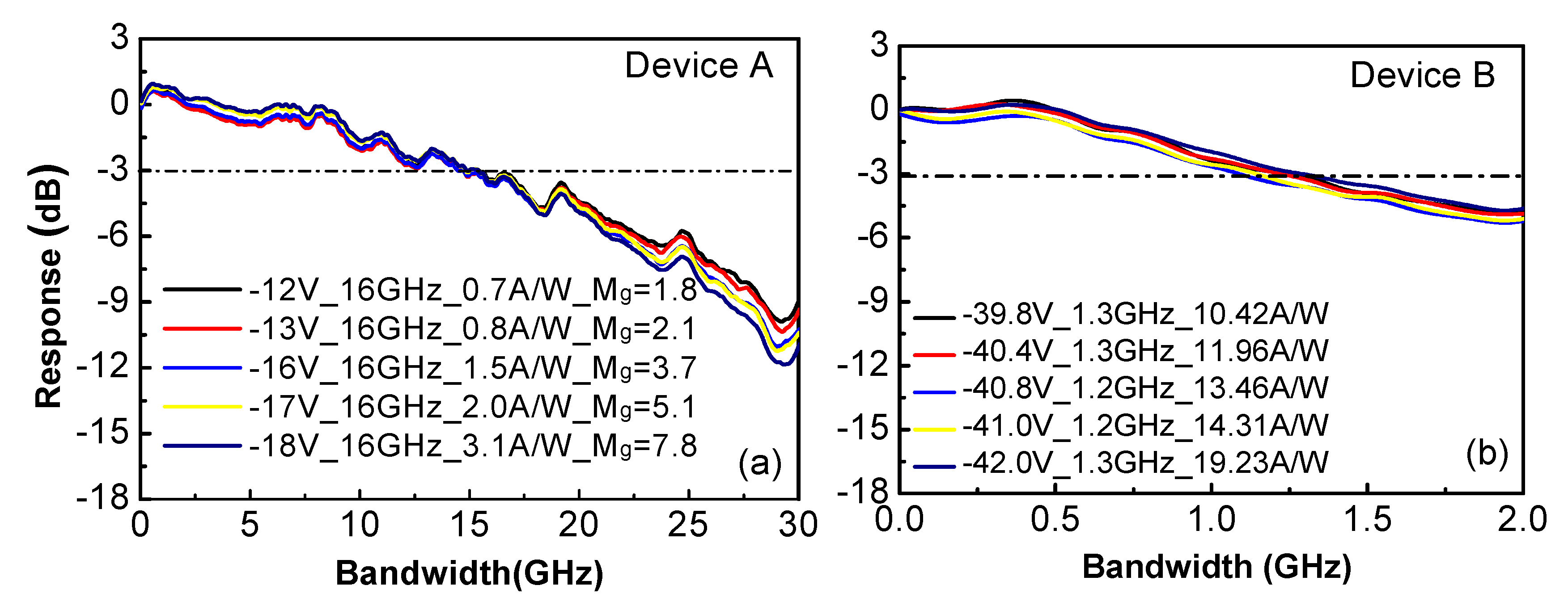
Figure 5a,b shows the bias dependent O-E frequency responses of Devices A and B measured under a high input optical power (1 mW and 240 μW), respectively. As can be seen, the 3-dB O-E bandwidths for devices A and B are pinned at 16 and 1.3 GHz, respectively, regardless of the changes in the reverse bias voltages. These bandwidth values are close to the maximum O-E bandwidths of the device measured under low power excitation, as shown in
Figure 4a,b. Such invariant high-speed performance can be attributed to the significant decrease in the value of the operation gain, becoming much less sensitive to the reverse bias voltage under high-power operation, as shown in
Figure 3a,b. The delay time induced by the avalanched gain, which is the major bandwidth limiting factor of an APD under high-gain (high-bias) operation is thus minimized, resulting in the observed invariance of the 3-dB O-E bandwidth [
11].
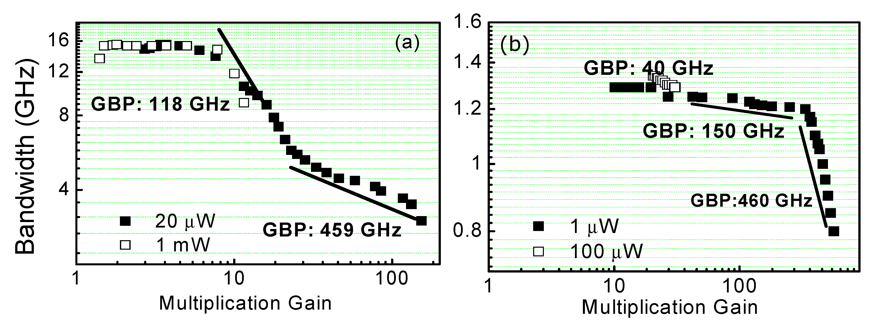
Figure 6a,b shows the 3-dB O-E bandwidth versus operation gain of Devices A and B, respectively, measured under low 20 (1) μW and high 1 (0.1) mW optical pumping power. As can be seen, for the low pumping power case, our demonstrated Device A can achieve a GBP as high as 459 GHz with a 38% unit-gain external efficiency and Device B has a GBP of around 460 GHz with a 1 A/W unit-gain external responsivity.
The maximum GBP values given here just follow the definitions reported for high-speed APDs [
6,
17] and these numbers suggest the maximum intrinsic speed of the APD [
6,
17]. However, for practical applications, APDs usually cannot be operated in such high-gain regions due to the increase of associated excess noise. Under 0.9 V
br operation, the corresponding GBP values for Devices A and B are around 122 (M
g = 8.7, 14 GHz) and 42 (M
g = 33.5, 1.25 GHz) GHz, respectively. On the other hand, there is a gradual decrease in the maximum values of the GBP to 118 and 40 GHz when the optical pumping power reaches 1 mW and 100 μW, respectively, which can be attributed to the reduction in the multiplication gain versus the increase of optical power, as discussed above. The high GBP of around 460 GHz achieved in our fabricated APDs can be attributed to effect of the multiplication layer, which is thinner than the conventional APD with its uniformly thick M-layer. Thus, localization impact ionization in the M-layer (in the lower M-layer) reduces the probability of the avalanche process occurring in the whole M-layer. In addition, the overall gain in our dual multiplication layer is higher, with each layer contributing to the gain, M1 and M2. Thus, the overall gain in our structure is M1*M2 to sustain a constant bandwidth. Furthermore, compared to the gain-bandwidth curves of typical APDs, which usually exhibit monotonic decreases of bandwidth with an increase in the multiplication gain [
3,
17], our device curves exhibit different trends. As can be seen for Device A, under a very-high operation gain (>30), the decrease in the bandwidth versus the gain is gradually minimized; for more details, please refer to our previous work [
11]. Our APD (Device B) demonstrates a constant O-E bandwidth (~1.25 GHz) over a wide range of operation gains (from 10 to ~300), which means a larger operation window.
Figure 7a,b shows the corresponding O-E responses measured under high-gain and low power operation. We can clearly see, the measured bandwidths for devices A and B are pinned at around 3 and 0.9 GHz, regardless of the gain. thereby resulting in the high gain-bandwidth product, as discussed above.
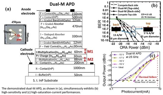
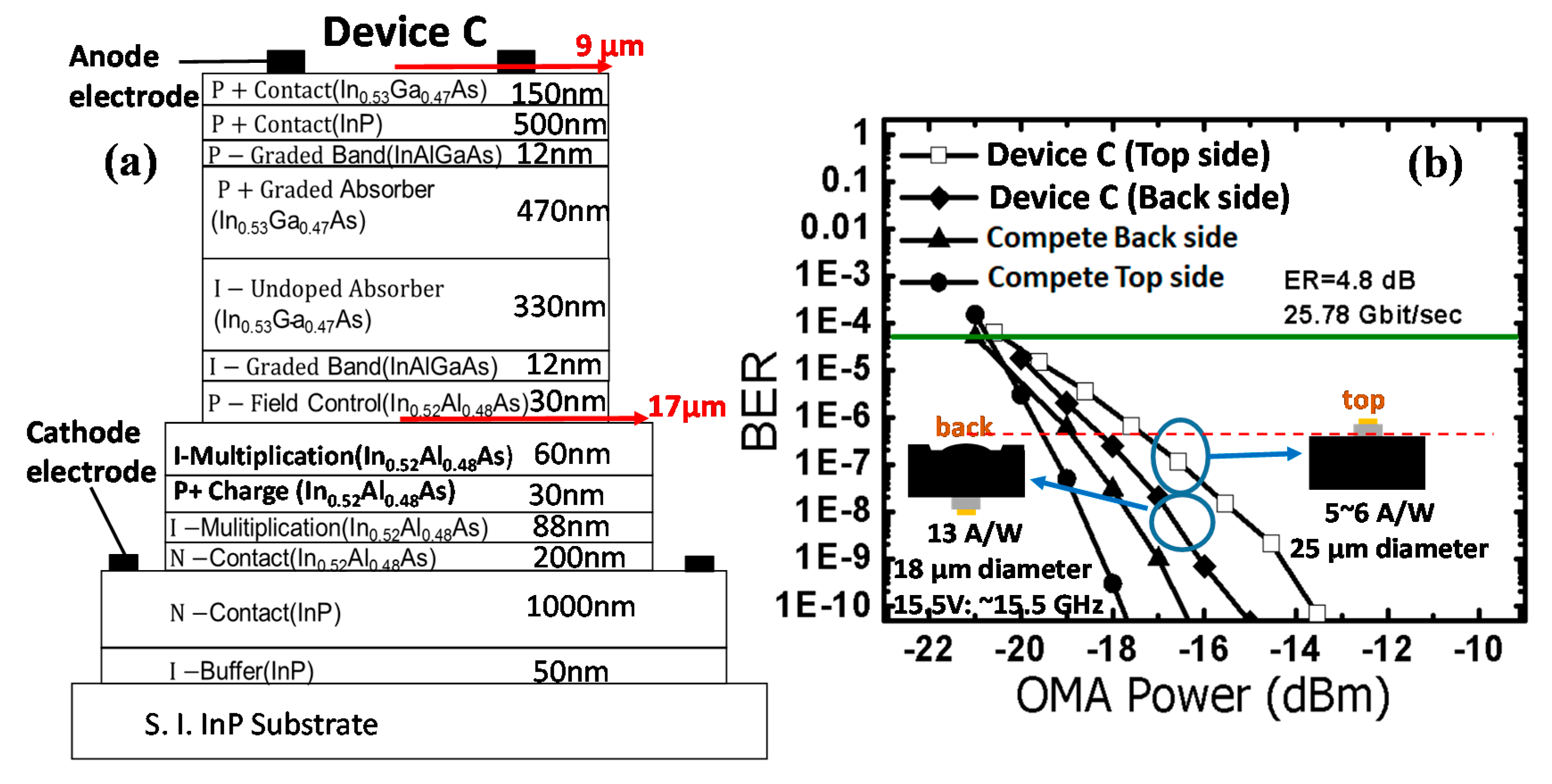
In order to further increase the responsivity of Device A for 100 GbE-ER4-Lite (40 km) applications, we increased the absorber layer thickness from 400 to 800 nm [
1] to fabricate device C.
Figure 8a shows conceptual cross-sectional views of the top-illuminated structure. This absorption layer thickness and the ratio of p-type/intrinsic layer thickness were chosen to balance the resistance-capacitance (RC) and transit time limited bandwidth [
1]. We conducted an APD bandwidth simulation based on our proposed linear model, which included the bandwidth limiting factors of the avalanche delay time, secondary hole transit time, and RC-delay time [
18]. For sensitivity measurement, samples of device C with both the top- and back-side illuminated structures were fabricated. These chips were integrated with 25 Gbit/s trans-impedance amplifiers (TIA) (Semtech; 200 Flynn Road, Camarillo, CA 93012. Product: GN1085) in a packaged ROSA module. During measurement, we adopted a commercial 25 Gbit/s electro-absorption modulated laser (EML) (2Source Photonics; 8521 Fallbrook Avenue #200, West Hills, CA 91304) to serve as the light source with a 4.8 dB extinction ratio (ER) adjusted to maintain the averaged power to be the same as the optical modulation amplitude (OMA).
Figure 8b shows the measured bit error rate (BER) values versus the OMA. A pseudorandom binary sequence (PRBS) of length 2
31–1 with a 25.78 Gbit/s date rate was used for testing. The green line shows the essential BER value (5 × 10
−5) needed to meet the KR4 forward error correction (FEC) coding. To measure BER, the APDs were integrated with a clock and data recovery (CDR) unit. The BER curves were measured using a commercially available APDs device integrated with the ROSA package [
4,
9] also shown for reference.
During BER measurement under 20 μW of optical input power, the optimized bias voltage of each ROSA module was near −15.5 and −16 V with a corresponding ∼6 and 13 A/W responsivity to obtain the highest sensitivity for the top- and back-side illuminated chips, respectively. Here, under the optimized bias point for high sensitivity operation, the corresponding GBP value of device C, with its backside-illuminated structure, is around 288 GHz (0.7 A/W for unit gain). The two structures achieved a sensitivity of around −20.6 dBm OMA which meets the specifications for 100 GbE-ER4-Lite (40 km) applications (40 km) [
19], which requires the receiver operate under a BER value of 5 × 10
−5 at an optical wavelength of 1.31 μm with a −18.5 dBm OMA sensitivity for 25 Gbit/s operation.
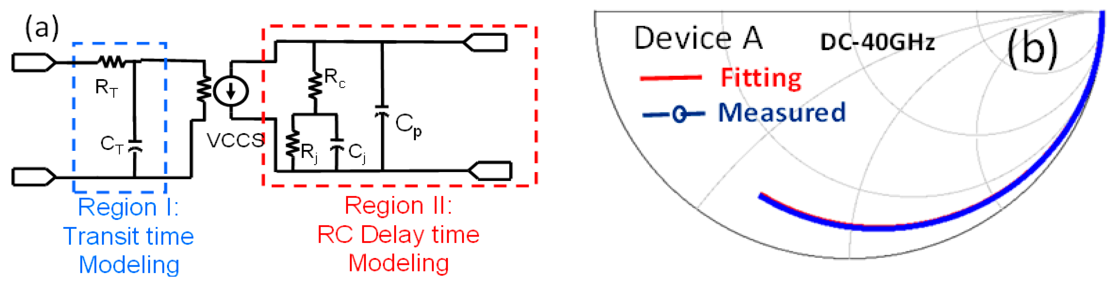
Of the three devices (A to C) studied here, Device A has the thinnest active layer, representing the fastest intrinsic speed performance. In order to further improve the high-speed performance of our APD structures (A to C), we utilized the equivalent-circuit modeling technique to investigate whether the carrier transit time or RC-bandwidth limits the speed of Device A.
Figure 9a shows the equivalent circuit models adopted for fitting of the microwave reflection coefficient (S
22) parameters for Device A.
The Smith chart in
Figure 9b shows the fitted and measured frequency responses corresponding to the S
22 parameters for Device A. Clearly, there is a good match between the simulated and measured results. The fitted values for each circuit element in Device A are shown in
Table 1. During the process of device modeling for the extraction of the extrinsic f
RC of the PD chips, the two artificial circuit elements, R
T and C
T, are removed. This is because they are used to mimic the low-pass frequency response of the internal carrier transient time [
16,
20]. By choosing the proper values of R
T and C
T to fit the measured O-E frequency response, we can then determine the internal transient time limited frequency responses of our devices.
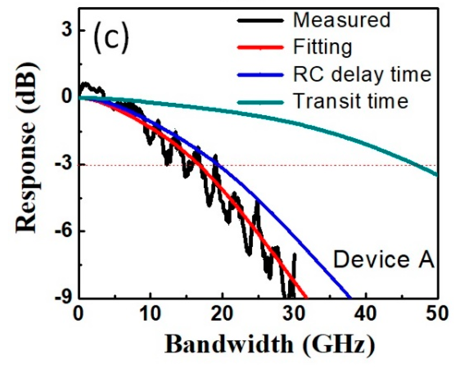
Figure 9c shows the measured O-E, fitted O-E, RC-limited and transient time limited frequency responses. As can be seen, under −13 V, Device A has an RC-limited O-E bandwidth. A wider 3-dB O-E bandwidth can be expected by further downscaling of the active diameter.
Thus, to further improve the bandwidth, we fabricated a back-illuminated device (Device A′) with a smaller active diameter of 18 versus 25 μm, share the same epi structure as that of Device A. The back-illuminated device offers the advantage of less coupling loss as compared to the top-illuminated device in which the top metal layer blocks light from entering the device [
5].
Figure 10a,c show top-views of the fabricated device before and after flip-chip bonding, respectively. Compared with our previous design [
21], the geometric size and layout of the flip-chip bonding co-planar waveguide (CPW) pads has further been optimized to not only minimize any ripples on the measured O-E frequency responses, but also to enhance the reliability of the flip-chip bonding process due to the increase in bonding area. We use gold-tin as the material for the bumps on the AlN substrate, because it has good thermal conductivity and low dielectric loss, for flip-chip bonding process.
Figure 10d shows the measured bias-dependent dark current, photocurrent, and operation gain of the demonstrated APDs, subject to different optical pumping powers at an optical wavelength of 1.31 μm. As can be seen, the measured breakdown voltage and punch through voltage are the same as for the top-illuminated counterpart.
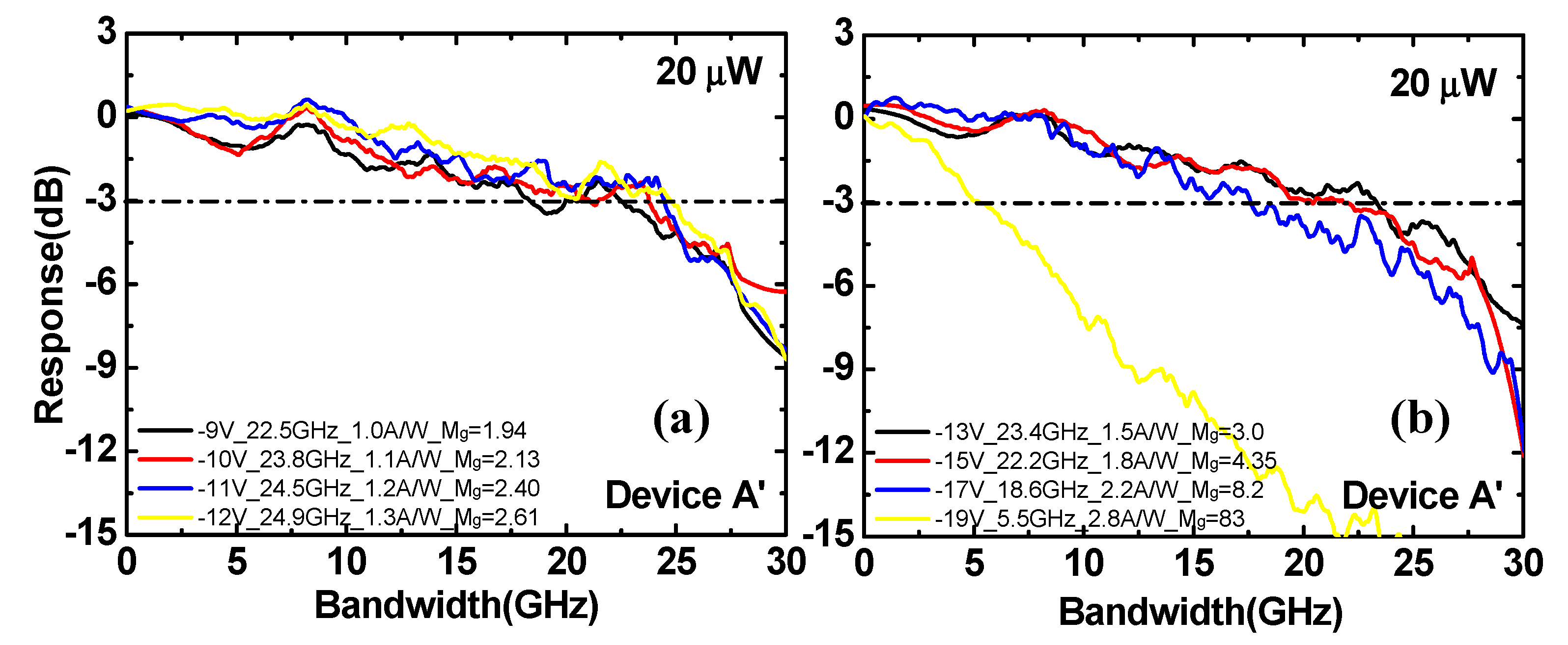
Figure 11a,b represents the bias dependent O-E frequency response of the back side illuminated Device A′ measured under an optical pumping power of 20 μW at the 1.3 1 μm wavelength. As can be seen, the measured 3 dB bandwidth of Device A′ is 24.5 GHz under low gain (Mg = 3) and 18.6 GHz under 0.9 V
br (Mg = 8.2). This is comparatively higher than those of the top illuminated device measured under the same operation gain condition. Here, we choose the responsivity (~0.51 A/W) at the punch-through point as our unit-gain responsivity. The corresponding GBP value under 0.9 V
br operation is around 153 GHz.
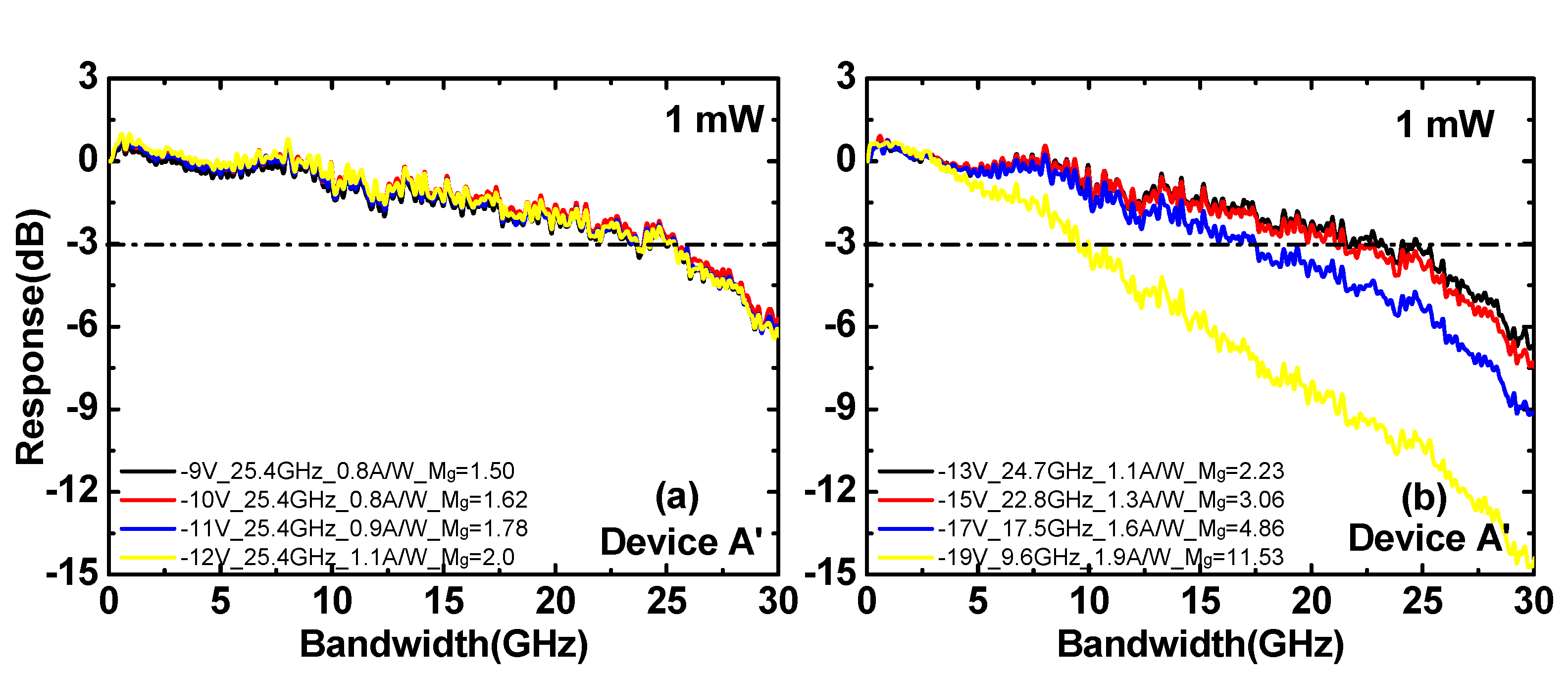
Figure 12a,b show the bias dependent O-E frequency responses of Device A′ measured under a high input optical power (1 mW). As can be seen, Device A′ behaves same as Device A. The maximum 3-dB O-E bandwidths are pinned at around 25 GHz, regardless of the changes in the reverse bias voltage. It is worth mentioning that under both low and high gain, our back side illuminated Device A′ has 6–8 GHz higher bandwidth compared to the top illuminated Device A.
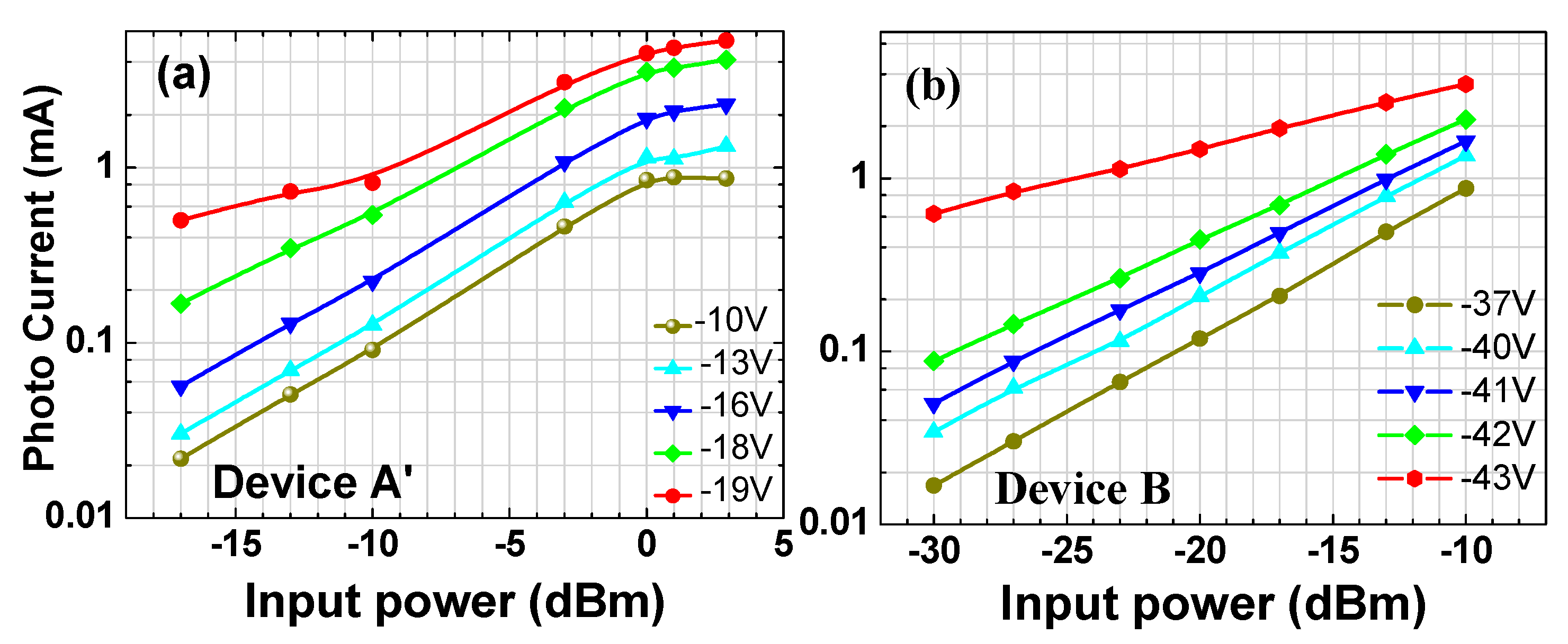
Figure 13a,b shows the dc output photocurrent versus the input optical power for Devices A′ and B, respectively. As can be seen, the dc saturation current of Device A′ is higher than that of Device B (5 versus 3 mA) at near V
br bias, due to the thinner depletion layer thickness. The output saturation power of our demonstrated APD is tested using a two-laser heterodyne-beating setup at the 1550 nm wavelength.
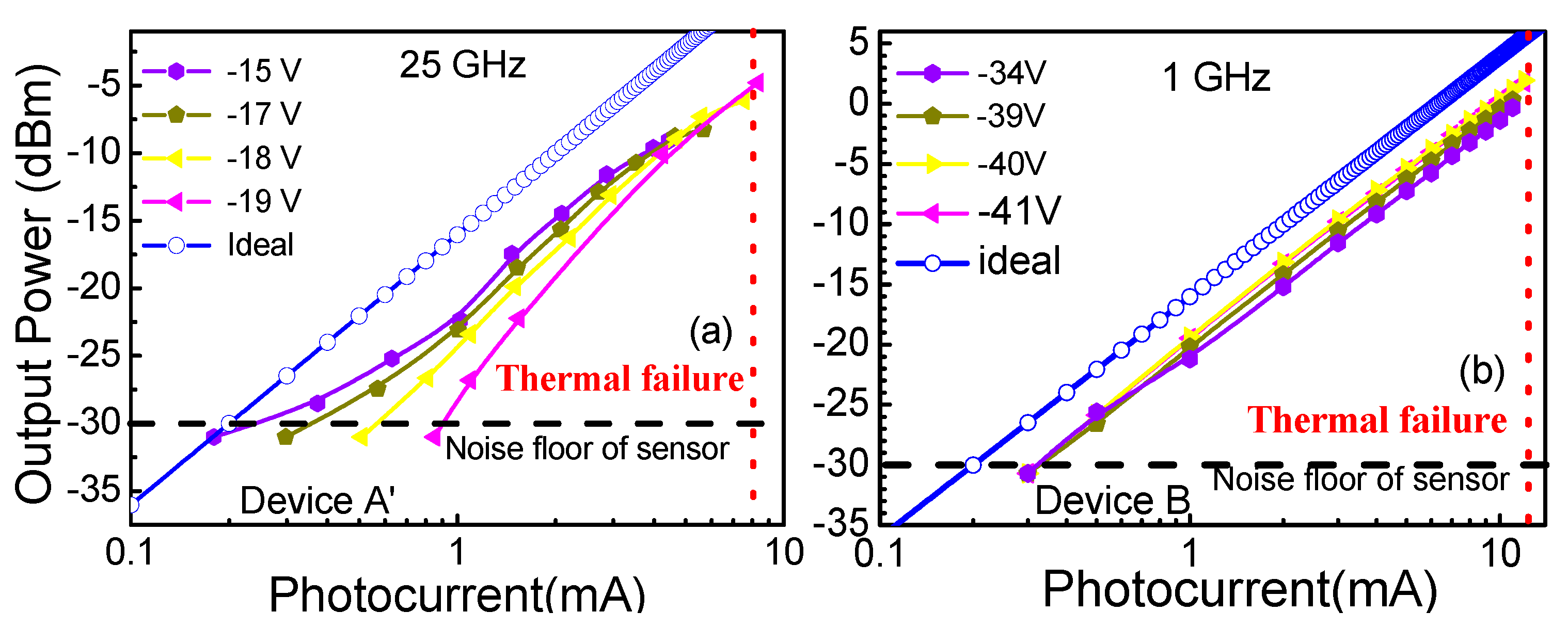
Figure 14a,b show the measured photo-generated radio frequency (RF) power versus output photocurrent obtained under different reverse biases. The measurement frequency was selected to be around the 3-dB O-E bandwidth for both Devices A′ and B at 25 GHz and 1 GHz, respectively. The ideal relation between the microwave power and averaged photocurrent (open symbol), with a 100% optical modulation depth under a 50 Ω load, is also plotted for reference.
We can clearly see that the photo-generated RF power of both Devices A′ and B shows no significant saturation even when the output photocurrent is above their dc saturation currents of 5 and 3 mA, respectively. Their maximum output powers are limited by thermal failure due to the high bias voltages required. Contrast this behavior with that of the typical high-speed p-i-n PDs, which always show saturation in the photo-generated RF power when their average output dc current is near saturation. In addition, under a small output photocurrent, the near V
br bias of both devices would lead to a photo-generated RF power far below the ideal power values on a 50 Ω load. As can be seen, the highest output photocurrents for maximum output RF power for Devices A′ and B occur at 8 and 12 mA, respectively. When the output photocurrent increases, all traces measured under different reverse bias voltages merge together, which can be attributed to the reduction in the avalanche delay time and enhancement of the O-E bandwidth under high-power operation, as discussed in
Figure 7a,b.

 ,
, 


