Article

The Optical Properties of InGaN/GaN Nanorods Fabricated on (-201) β-Ga2O3 Substrate for Vertical Light Emitting Diodes

1
State Key Laboratory of Solid-State Lighting, Institute of Semiconductors, Chinese Academy of Sciences, Beijing 100083, China
2
Center of Materials Science and Optoelectronics Engineering, University of the Chinese Academy of Sciences, Beijing 100049, China
*
Author to whom correspondence should be addressed.
Photonics 2021, 8(2), 42; https://doi.org/10.3390/photonics8020042
Submission received: 29 December 2020 / Revised: 29 January 2021 / Accepted: 2 February 2021 / Published: 6 February 2021
(This article belongs to the Special Issue Wide Bandgap Semiconductor Photonic Devices)

Abstract

:
We fabricated InGaN/GaN nanorod light emitting diode (LED) on (-201) β-Ga2O3 substrate via the SiO2 nanosphere lithography and dry-etching techniques. The InGaN/GaN nanorod LED grown on β-Ga2O3 can effectively suppress quantum confined Stark effect (QCSE) compared to planar LED on account of the strain relaxation. With the enhancement of excitation power density, the photoluminescence (PL) peak shows a large blue-shift for the planar LED, while for the nanorod LED, the peak position shift is small. Furthermore, the simulations also show that the light extraction efficiency (LEE) of the nanorod LED is approximately seven times as high as that of the planar LED. Obviously, the InGaN/GaN/β-Ga2O3 nanorod LED is conducive to improving the optical performance relative to planar LED, and the present work may lay the groundwork for future development of the GaN-based vertical light emitting diodes (VLEDs) on β-Ga2O3 substrate.

1. Introduction

The light emitting diodes (LEDs) have the characteristics of small size, high efficiency, energy conservation, long lifetime, and so on, which have great attracted attention and interest from both scientific and industrial communities in recent years [1,2]. Generally, GaN is an ideal material, and nitride-based devices are heteroepitaxially grown on sapphire, SiC or Si substrates. Although heteroepitaxial growth of GaN on sapphire is well established, sapphire does not represent an adequate candidate because it has insulation characteristic, and has a 14% lattice mismatch which causes high dislocation density [3]. Another routinely used substrate, SiC, has a much smaller lattice mismatch (3.1%) compared with sapphire [4]. Nevertheless, SiC is expensive and has high optical losses owing to the lack of transparency [5]. Therefore, it is important to find an alternative substrate which can be used to fabricate light emitting diode (LED) devices with good lattice match, low dislocation density, appropriate optical and electrical properties, as well as high transparency in visible spectrum regions.
As the group of transparent conductive oxides, the β-gallium oxide (β-Ga2O3) has an ultrawide bandgap (Eg ≈ 4.6–4.9 eV) [6,7,8,9] and thus exhibits a unique transparency from the visible into the ultraviolet (UV) region. In other words, the transparent nature of β-Ga2O3 as a substrate provides a wider light-emitting area than conductive SiC or Si substrates. In addition, monoclinic β-Ga2O3 also has the characteristics of high breakdown electric field (~8 MV/cm) [10], excellent thermal and chemical stability and so on, attracting a lot of attention due to its wide range of potential applications in short wavelength photonics, transparent electronics, power devices and optoelectronic devices. Meanwhile, the lattice mismatch between β-Ga2O3 and GaN is found to be small, is ~4.7% [5,11]. The electrical conductivity of β-Ga2O3 can be achieved by doping. In addition, its conductivity can be adjusted on the basis of the demands [12]. Thus, the β-Ga2O3 can serve as a good substrate candidate for the growth of GaN because the β-Ga2O3 substrate combines the beneficial properties (transparency, good lattice match, and conductivity) of sapphire, SiC or Si substrates. Recently, we also carried out some works of GaN layer grown on β-Ga2O3 substrate [13,14,15]. However, there are still many problems existing in the LEDs based on β-Ga2O3 substrate. One is the lattice mismatch between GaN and β-Ga2O3, still resulting in strong quantum confined Stark effect (QCSE) in multiple quantum wells (MQWs) of LEDs. Another is the low light extraction efficiency (LEE), owing to high refractive index between GaN (n ≈ 2.5) [16] and air (n = 1), as well as high refractive index between β-Ga2O3 (n = 1.68~1.89) [17] and air (n = 1). Thus, most of the light emitted from MQWs is trapped in the devices, leading to the huge light loss [18]. So the LEE of the planar LED is usually low. Generally speaking, nanorod or nanowire LEDs are deemed to a viable solution to unravel long pending issues such as QCSE, inefficient light extraction and so on. Particularly on the issue of QCSE, the changes in the internal field and strain can affect its magnitude, resulting in change of the bandgap. The nanorod or nanowire LEDs can release the internal strain, as well as suppress the lateral transport of carriers in MQWs [19]. Besides, the LEE of the nanorod or nanowire LEDs may also be effectively improved since they avoid total internal reflection and prevent the lateral propagation of light-waveguide effects [20].
Therefore, based on these features, we fabricated the InGaN/GaN nanorod LED on β-Ga2O3 substrate for vertical LED (VLED) by the SiO2 nanosphere lithography and dry-etching techniques. Depending on the Raman measurements, the compressive strain in the planar and nanorod LED can be estimated to be 0.26 GPa and 0.07 GPa, respectively, illustrating the nanorod LED is more close to strain-free state relative to planar LED. Due to the reduction in the QCSE, the scattering and high LEE, the photoluminescence (PL) peak intensity value of the nanorod LED is obviously stronger than that of the planar LED. As the excitation power density of PL increases, emission peak position of the planar LED obviously blue-shifts, while there is slightly shift for the peak position of the nanorod LED. Furthermore, the LEE of the nanorod LED is also effectively improved compared with the planar LED on β-Ga2O3 substrate.

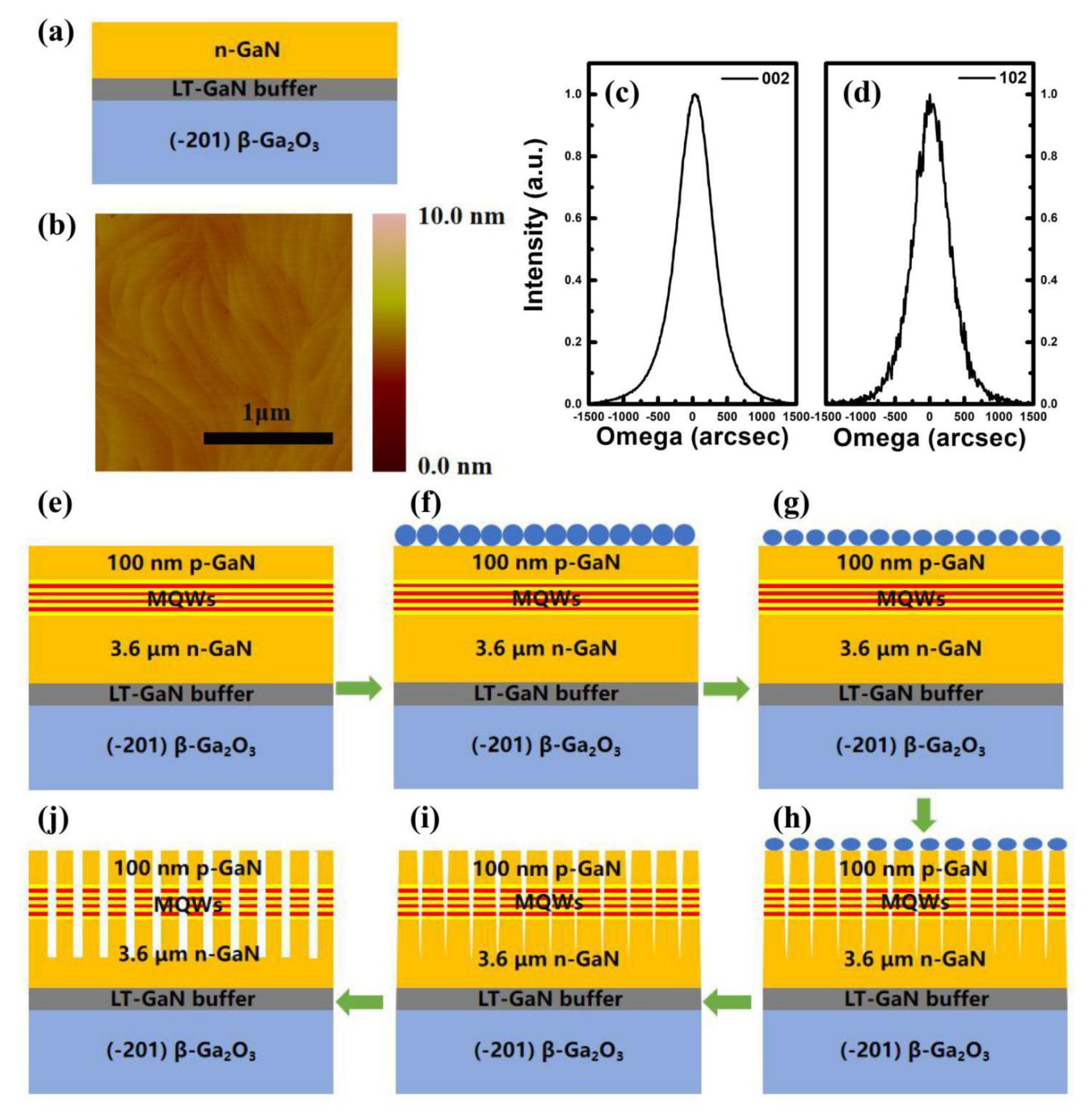
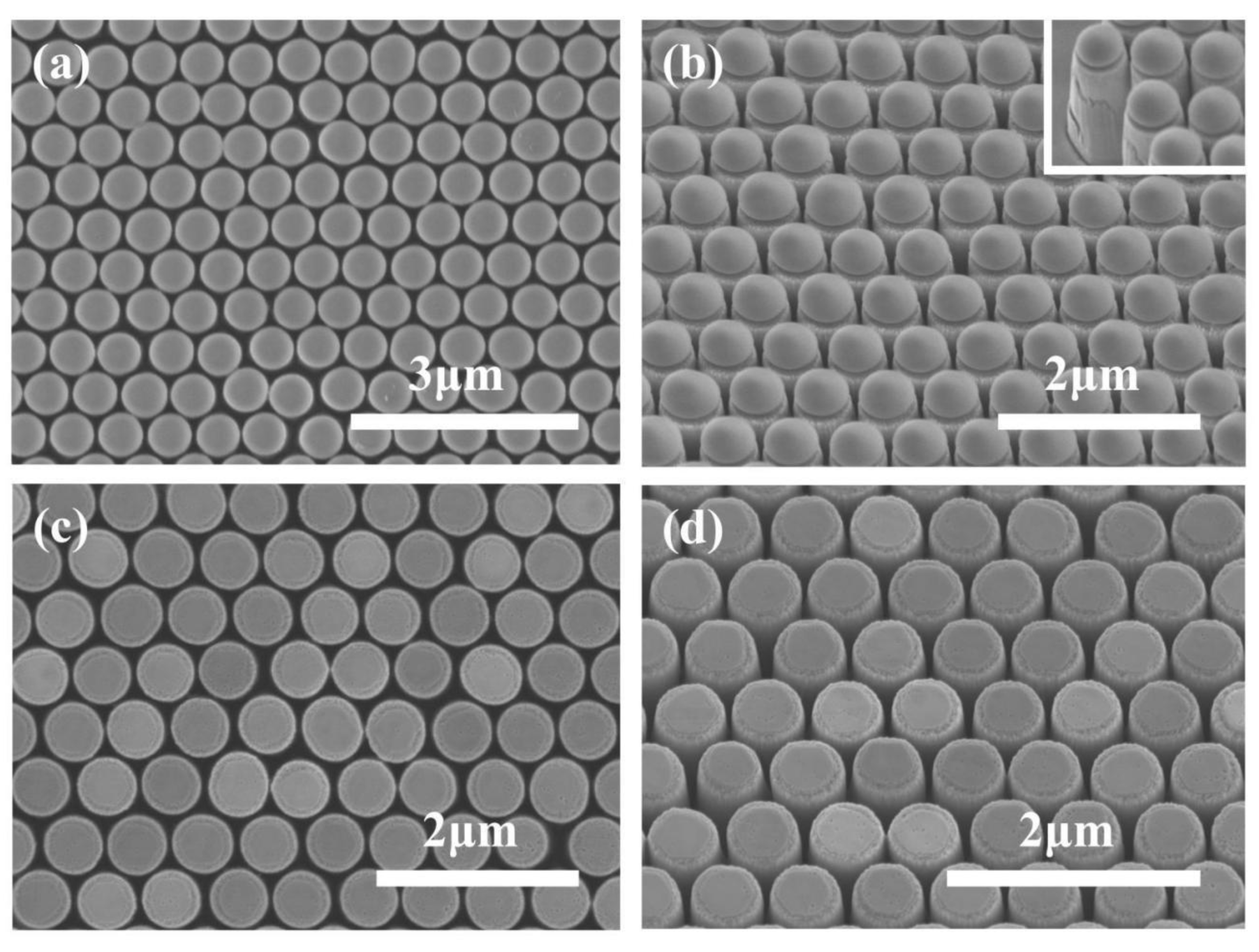
2. Experimental Procedures

Firstly, in order to avoid the β-Ga2O3 substrate being etched by H2, the low-temperature undoped GaN (LT-GaN) buffer layer was grown at 525 °C under an N2 atmosphere on (-201)-oriented monoclinic conductive β-Ga2O3 substrate using a 500 Torr pressure by metal organic chemical vapor deposition (MOCVD), and the thickness was approximately 12 nm. After changing the carrier gas from N2 to H2, a pulse growth procedure was employed, which mainly reduces threading dislocation and improves the crystalline quality of GaN [15]. When the temperature of the substrate was increased to 1020 °C, the pulse layer was grown. For the pulse layer, NH3 was inputted by the pulse flow method under circumstance of 200 Torr, and each cycle was 0.3 min. However, it was worth noticing that the Ga source remained normally open, while the NH3 source was only opened in the last 0.2 min in each cycle, and had 200 cycles in total. The temperature was further increased to 1080 °C during the deposition of the remainder of the n-type doped GaN (n-GaN) layer. The total thickness of n-GaN layer was approximately 3.6 μm. Figure 1a shows the schematic diagram of the LT-GaN buffer layer and n-GaN layer grown on the (-201) β-Ga2O3 substrate. Figure 1b shows the atomic force microscopy (AFM) image result for 2 × 2 μm2 of the epitaxial GaN on β-Ga2O3 substrate. The smooth step-like morphology can be seen, with the root-mean-square (RMS) roughness of approximately 0.187 nm. The Figure 1c,d show the X-Ray diffraction (XRD) rocking curves of the epitaxial GaN on β-Ga2O3 substrate. The full width at half maximum (FWHM) of GaN (002) and (102) reflection peaks are approximately 599.4 and 546.6 arcsec, respectively. This means that GaN can be successfully grown on β-Ga2O3 substrate. Then the five periods of InGaN/GaN MQWs and the approximately 100 nm thick p-type doped GaN (p-GaN) layer were epitaxially grown on the n-GaN layer.
First of all, the sample was cleaned by the mixed solution of sulfuric acid and hydrogen peroxide (H2SO4:H2O2 = 3:1). Then the nanospheres mixed solution was made via mixing the original solution of the SiO2 nanospheres, deionised water and ethyl alcohol (1:1:1). The nanospheres mixed solution was put into the ultrasonic apparatus and oscillated for 20 min to further mix. Next, adding a large amount of water and 50 μL hydrochloric acid to the quartz container. The glass slide was placed in the edge of the container at a certain inclined angel, and nanospheres mixed solution was slowly dripped on the glass slide via the pipetting gun, until a monolayer SiO2 film was formed on the surface of the water in the container. Following that, a drop of the sodium dodecyl benzene sulfonate (SDBS) solution was added into the water, resulting in more ordered and compact arrangement of the SiO2 nanospheres. The sample was placed into the water at about 45° angle and slowly moved to the bottom of the monolayer SiO2 film along the horizontal direction. Then the sample was slowly pulled up from bottom to top with hand or puller. In this way, a highly ordered self-assembled monolayer of SiO2 nanospheres was dip-coated on the sample. Finally, the sample was placed in a place without air flow.
Figure 1e–j show the fabrication flow diagrams of the nanorod LED using the SiO2 nanosphere lithography and dry-etching techniques. In the first place, in accordance with the above method, a highly ordered self-assembled monolayer of SiO2 nanospheres with the diameter of 660 nm was dip-coated on the planar LED with epitaxial grown on β-Ga2O3 substrate. Subsequently, the diameter of SiO2 nanospheres was shrunk to approximately 580 nm on the sample via CHF3-based inductively coupled plasma (ICP) dry-etching. Because the GaN was etched using Cl-based gas and the etching ratio (Si/GaN) was small, these SiO2 nanospheres could be used as mask and protect the top p-GaN layer. Then the sample was etched down to the n-GaN layer via Cl-based ICP etching, with the etching depth of approximately 1.4 μm. Next, the SiO2 mask was removed via the buffer oxide etchant (BOE) solution and the nanorod LED was obtained. Finally, the nanorod LED was treated in the potassium hydroxide (KOH) solution.

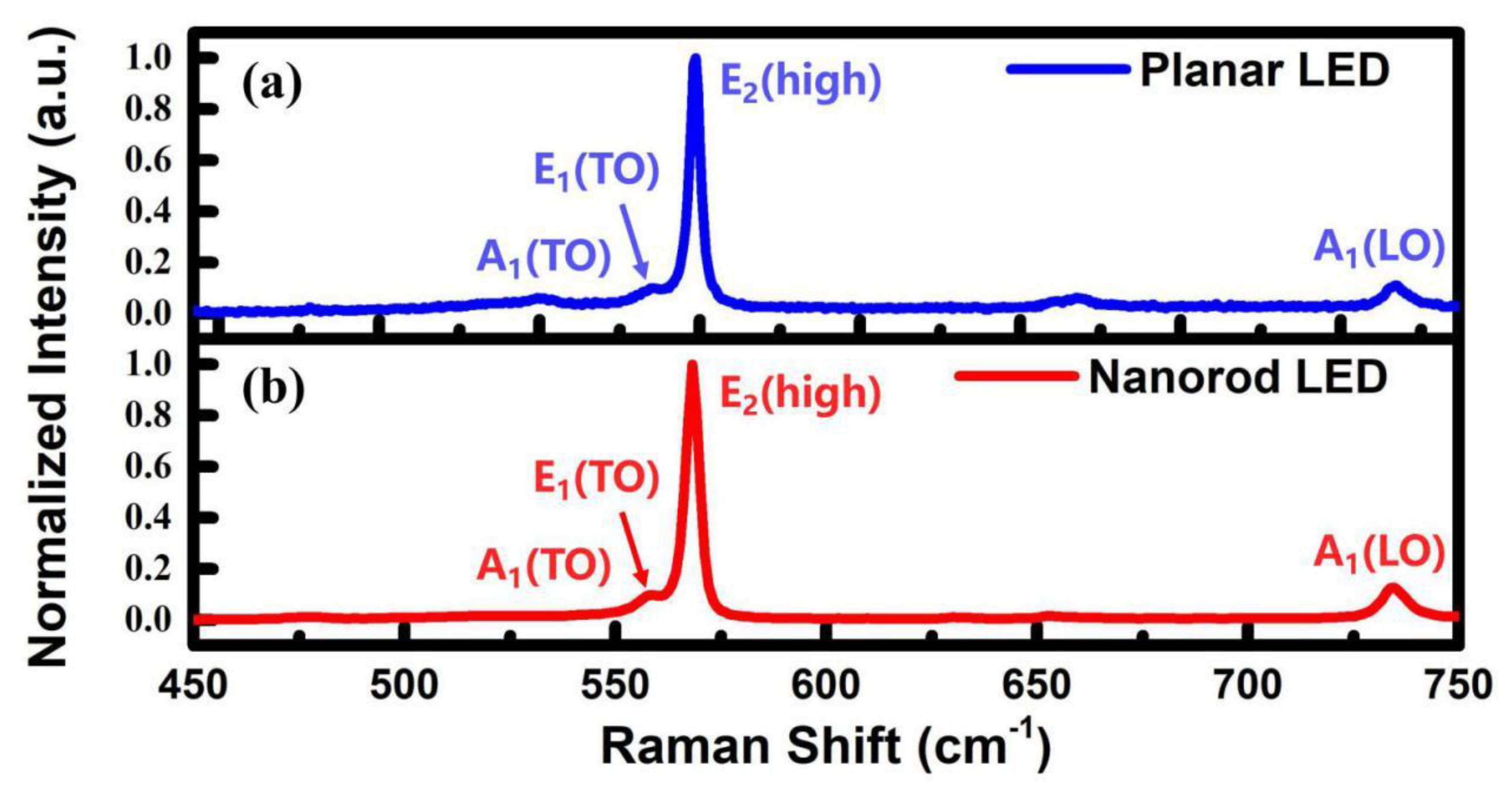
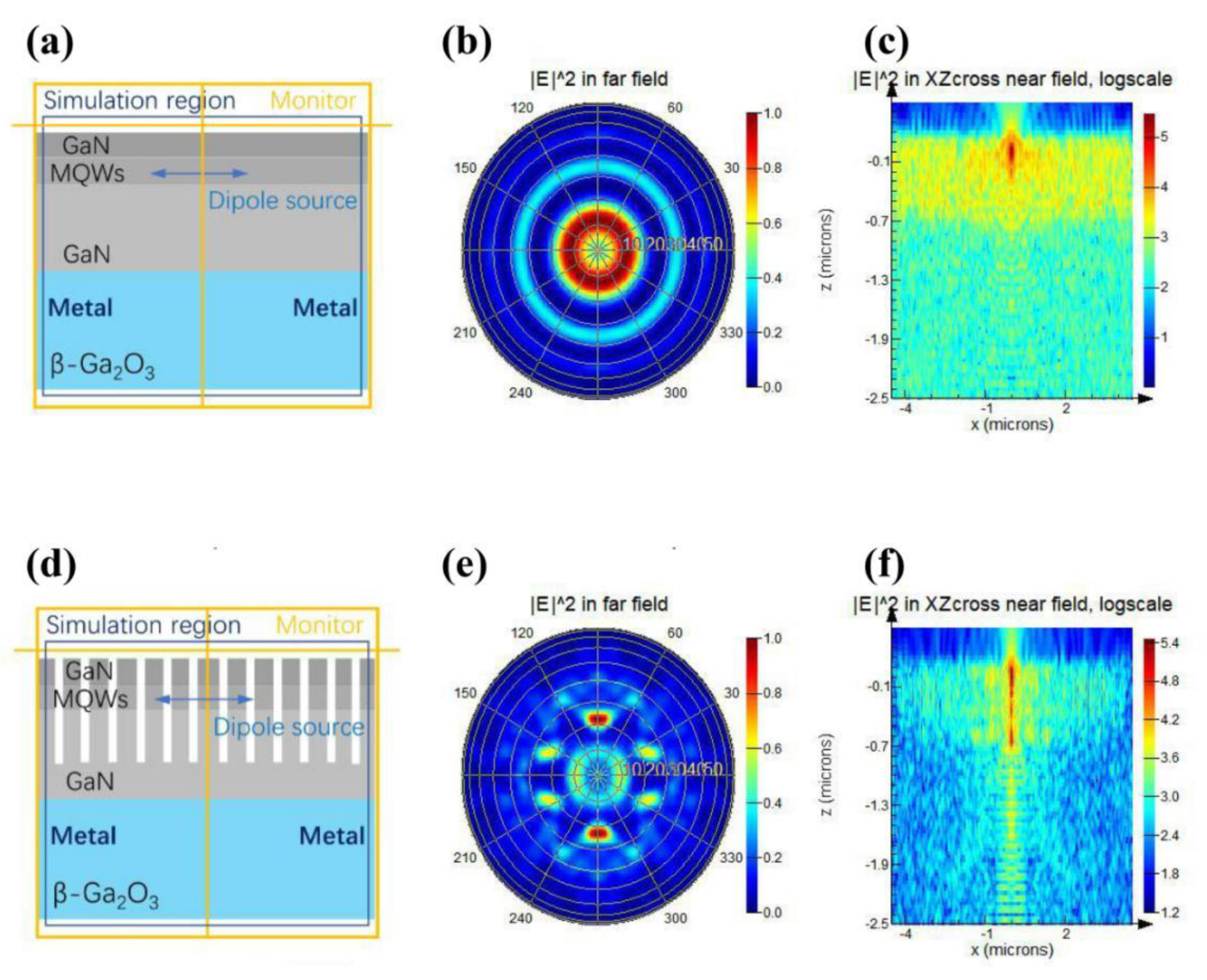
3. Results and Discussion

The Figure 2a–d show the scanning electron microscopy (SEM) images of nanorod LED on (-201) β-Ga2O3 substrate before and after removing SiO2 nanospheres. It can be seen that the nanorod arrays are well arranged in an orderly manner. The top diameter is approximately 580 nm, and there is enough space between the nanorods. For the sake of removing ICP-induced etching damages on the sidewall surface of the nanorods, the sample is dipped into KOH solution with the concentration of 5% for 2 min.
In order to verify whether the strain of nanorod LED on β-Ga2O3 substrate is released or not, the Raman measurements of the GaN/β-Ga2O3 planar and nanorod LED are revealed, respectively, with a range of 450–750 cm−1 [21,22]. The results are shown in Figure 3a,b. The observed peaks are mainly A1(TO), E1(TO), E2(high) and A1(LO) mode peaks of GaN. In the general case, the E2(high) phonon mode of GaN is sensitive to strain within the material [23]. Therefore, strain state in GaN epitaxial layer can be characterized by the peak position of the E2(high) phonon mode. Here, we clearly observe that the peak position of the E2(high) phonon mode within the GaN/β-Ga2O3 planar and nanorod LED. The peak positions of the E2(high) phonon mode within the GaN/β-Ga2O3 planar and nanorod LED are located at approximately 569.1 cm−1 and 568.3 cm−1, respectively. We can conclude that there clearly exist compressive strain because the peak positions of the planar and nanorod LED exhibit a red-shift of 1.1 cm−1 and 0.3 cm−1, respectively, relative to the bulk GaN (568 cm−1) [24]. The strain σ in the GaN film can be calculated via the following formula: σ = Δω/k. In this equation, Δω is the Raman shift from the E2(high) phonon mode of the strain-free GaN film, and k is the Raman strain factor. Here, k = 4.2 cm−1/GPa is adopted [25]. The strain σ in the GaN epitaxial layer of the planar and nanorod LED can be estimated to be 0.26 GPa and 0.07 GPa, respectively. It also means that the planar LED is in a state of highly compressive strain. Therefore, the nanorod LED is more close to strain-free state, indicating the alleviated QCSE.
Figure 4a shows the PL spectrum of the GaN/β-Ga2O3 planar and nanorod LED under the room temperature, and can be expressed by logarithmic coordinates. It can be seen that, under the same excitation condition, the peak positions of the planar and nanorod LED are located at 424.2 and 422.8 nm, respectively. Obviously, the peak wavelength position of nanorod LED shows blue-shift of about 1.4 nm relative to planar LED. It proves that the strain is released at a certain extent, indicating that the QCSE can be relieved. The reduced QCSE enables the relieved band bending, the increased wave function overlap of electrons and holes, and therefore increases internal quantum efficiency (IQE) [26]. It can be noticed that PL peak intensity value for the nanorod LED is higher than that of the planar LED. When the nanorod LED is excited by PL, the light from the excitation source can be scattered between adjoining nanorods, leading to the increased the probability of extracted photons. In addition, the nanorod LED shows high LEE, which enables more light generated from the active region and results in the strong PL peak intensity value. Therefore, the enhancement of the PL peak intensity value for the nanorod LED is considered as a consequence the combined effects of the reduction in the QCSE, the scattering and high LEE.
Figure 4b,c show the PL spectrum of the GaN/β-Ga2O3 nanorod and planar LED under the different excitation power densities which increases from 1% to 100% (The maximum excitation power density value of the light source is approximately 9.55 kW/cm2). The number of photogenic electron-hole pairs increases with the enhancement of excitation power density, resulting in the increased PL peak intensity values of the nanorod and planar LED. The curves of the extracting values of the peak wavelength position and the FWHM under different excitation power densities are shown in Figure 4d,e. For the planar LED, the position of the PL peak wavelength obviously shifts to shorter wavelength (from 437.6 to 425.1 nm) with the enhancement of excitation power density, but there is a slightly red-shift (425.9 nm) at 100% excitation power density. For the nanorod LED, the peak wavelength position shows a slight red-shift as increasing the excitation power density from 0 to 1 kW/cm2, which may be caused by the self-heating with the enhancement of excitation power density. The shift of peak wavelength position may be negligible with the increase in excitation power density from 1 to 9.55 kW/cm2. Besides, under the same excitation power density, the peak wavelength position of the nanorod LED is shorter than that of the planar LED, indicating the strain relaxation within the nanorod LED. It can also be seen that as the excitation power density increases, the FWHM of the planar LED and nanorod LED become narrowed, as shown in Figure 4e. The FWHM of the planar LED drops markedly from 80.93 to 33.69 nm, while the FWHM of the nanorod LED drops slightly from 27.97 to 21.17 nm. This is mainly because the screening effects of the piezoelectric field is continuously enhanced by increased carriers with the enhancement of excitation power density [27].
According to finite-difference time domain (FDTD) simulation, the nanorod LED can also significantly improve the LEE. Figure 5a–c and Figure 5d–f show the FDTD simulation results of the planar and nanorod LED on (-201) β-Ga2O3 substrate, respectively. The simulation structure including 2 μm Ga2O3 substrate, 600 nm n-GaN, 100 nm MQWs, 100 nm p-GaN, the nanorods with the diameter of the 580 nm, respectively, as well as the refractive index and the extinction coefficient of the corresponding materials are imported. For the planar LED, most of the light emitted from MQWs is trapped in the epitaxial layer and substrate because photons emitting outside the range of the critical angle are totally reflected at the GaN–air and β-Ga2O3–air interface. On the contrary, for the nanorod LED, emitted light from MQWs is no longer confined to the escape cone. The nanorod LED forms quasi waveguide structure, and the light emitted from the MQWs of one individual nanorod can couple into the vertically directed guided mode [28], or couple into adjoining nanorods to again form vertically directed guided mode, leading to the increased chance of photons escaping from the substrate side. Moreover, the Bragg diffraction induced by the highly ordered nanorod LED also increases the photons extracted from the sidewall in the vertical direction [29]. Still having a bit is, the downsize with the p-GaN leads to the decrease with the absorption of photons, and thereby increases the escaping probability of the photon from the inside of the chip [26]. Therefore, on the basis of the simulation results, the LEE value of the nanorod LED is 61.51%, which is much higher than that of planar LED with the value of 8.89%.

4. Conclusions

In summary, we have fabricated GaN/β-Ga2O3 nanorod LED via the SiO2 nanosphere lithography and dry-etching techniques. Compared to planar structure, the strain can be relaxed owing to the formation of nanorod LED. The results of the PL measurement show the increased luminescence intensity value for the nanorod LED compared to that of planar LED. As the excitation power density increases, the peak wavelength of the nanorod LED slightly shifts, while the PL peak wavelength of planar LED greatly blue-shifts, and the FWHM becomes narrow for both. In the meantime, we also perform the FDTD simulations to explore the LEE improvement of nanorod LED. The GaN/β-Ga2O3 nanorod LED is expected to pave the way toward reliable and bright vertical-injection GaN-based LEDs.

Author Contributions

Conceptualization, J.Z., W.L. and T.W.; methodology, J.Z. and W.L.; software, W.L.; validation, J.Z., W.L. and T.W.; formal analysis, J.Z., W.L. and L.W.; investigation, J.Z. and W.L.; resources, X.W., J.W. and T.W.; writing—original draft preparation, J.Z.; writing—review and editing, T.W.; supervision, T.W.; project administration, X.W., J.W. and T.W.; funding acquisition, X.W., J.W. and T.W. All authors have read and agreed to the published version of the manuscript.

Funding

This research was funded by the National Key R&D Program of China (No. 2018YFB0406702), the National Natural Science Foundation of China (No. 61974139) and the Beijing Natural Science Foundation (No. 4182063).

Conflicts of Interest

The authors declare no conflict of interest.

References

  1. Min, D.; Park, D.; Jang, J.; Lee, K.; Nam, O. Phosphor-free white-light emitters using in-situ GaN nanostructures grown by metal organic chemical vapor deposition. Sci. Rep. 2015, 5, 17372. [Google Scholar] [CrossRef] [Green Version]
  2. Zhao, J.; Wei, T.; Zhang, J.; Zhang, Y.; Wei, X.; Yan, J.; Wang, J.; Li, J. Phosphor-free three-dimensional hybrid white LED with high color-rendering index. IEEE Photonics J. 2019, 11, 8200608. [Google Scholar] [CrossRef]
  3. Muhammed, M.M.; Roldan, M.A.; Yamashita, Y.; Sahonta, S.L.; Ajia, I.A.; Iizuka, K.; Kuramata, A.; Humphreys, C.J.; Roqan, I.S. High-quality III-nitride films on conductive, transparent (-201)-oriented β-Ga2O3 using a GaN buffer layer. Sci. Rep. 2016, 6, 29747. [Google Scholar] [CrossRef] [Green Version]
  4. Liu, L.; Edgar, J.H. Substrates for gallium nitride epitaxy. Mater. Sci. Eng. R 2002, 37, 61–127. [Google Scholar] [CrossRef]
  5. Muhammed, M.M.; Peres, M.; Yamashita, Y.; Morishima, Y.; Sato, S.; Franco, N.; Lorenz, K.; Kuramata, A.; Roqan, I.S. High optical and structural quality of GaN epilayers grown on (-201) β-Ga2O3. Appl. Phys. Lett. 2014, 105, 042112. [Google Scholar] [CrossRef] [Green Version]
  6. Bin Anooz, S.; Grüneberg, R.; Wouters, C.; Schewski, R.; Albrecht, M.; Fiedler, A.; Irmscher, K.; Galazka, Z.; Miller, W.; Wagner, G.; et al. Step flow growth of β-Ga2O3 thin films on vicinal (100) β-Ga2O3 substrates grown by MOVPE. Appl. Phys. Lett. 2020, 116, 182106. [Google Scholar] [CrossRef]
  7. Kim, M.; Huang, H.C.; Kim, J.D.; Chabak, K.D.; Kalapala, A.R.K.; Zhou, W.; Li, X. Nanoscale groove textured β-Ga2O3 by room temperature inverse metal-assisted chemical etching and photodiodes with enhanced responsivity. Appl. Phys. Lett. 2018, 113, 222104. [Google Scholar] [CrossRef]
  8. Lee, M.H.; Peterson, R.L. Accelerated Aging Stability of β-Ga2O3-Titanium/Gold Ohmic Interfaces. ACS Appl. Mater. Interfaces 2020, 12, 42677–46287. [Google Scholar] [CrossRef]
  9. Chen, J.; Li, X.; Ma, H.; Huang, W.; Ji, Z.; Xia, C.; Lu, H.; Zhang, D.W. Investigation of the Mechanism for Ohmic Contact Formation in Ti/Al/Ni/Au Contacts to β-Ga2O3 Nanobelt Field-Effect Transistors. ACS Appl. Mater. Interfaces 2019, 11, 32127–32134. [Google Scholar] [CrossRef]
  10. Singh, R.; Lenka, T.R.; Velpula, R.T.; Jain, B.; Bui, H.Q.T.; Nguyen, H.P.T. Investigation of current collapse and recovery time due to deep level defect traps in β-Ga2O3 HEMT. J. Semicond. 2020, 41, 102802. [Google Scholar] [CrossRef]
  11. Víllora, E.G.; Shimamura, K.; Kitamura, K. Epitaxial relationship between wurtzite GaN and β-Ga2O3. Appl. Phys. Lett. 2007, 90, 234102. [Google Scholar] [CrossRef]
  12. Ueda, N.; Hosono, H. Synthesis and control of conductivity of ultraviolet transmitting β-Ga2O3 single crystals. Appl. Phys. Lett. 1997, 70, 3561–3563. [Google Scholar] [CrossRef]
  13. Li, W.; Zhang, X.; Meng, R.; Yan, J.; Wang, J.; Li, J.; Wei, T. Epitaxy of III-Nitrides on β-Ga2O3 and Its Vertical Structure LEDs. Micromachines 2019, 10, 322. [Google Scholar] [CrossRef] [Green Version]
  14. Li, W.; Zhang, X.; Zhao, J.; Yan, J.; Liu, Z.; Wang, J.; Li, J.; Wei, T. Rectification behavior of polarization effect induced type-II n-GaN/n-type β-Ga2O3 isotype heterojunction grown by metal organic vapor phase epitaxy. J. Appl. Phys. 2020, 127, 015302. [Google Scholar] [CrossRef]
  15. Li, W.; Guo, L.; Zhang, S.; Hu, Q.; Cheng, H.; Wang, J.; Li, J.; Wei, T. (100)-Oriented gallium oxide substrate for metal organic vapor phase epitaxy for ultraviolet emission. CrystEngComm 2020, 22, 3122–3129. [Google Scholar] [CrossRef]
  16. Billeb, A.; Grieshaber, W.; Stocker, D.; Schubert, E.F. Microcavity effects in GaN epitaxial films and in Ag/GaN/sapphire structures. Appl. Phys. Lett. 1997, 70, 2790–2792. [Google Scholar] [CrossRef] [Green Version]
  17. Pearton, S.J.; Yang, J.; Cary IV, P.H.; Ren, F.; Kim, J.; Tadjer, M.J.; Mastro, M.A. A review of Ga2O3 materials, processing, and devices. Appl. Phys. Rev. 2018, 5, 011301. [Google Scholar] [CrossRef] [Green Version]
  18. Zhao, J.; Wei, X.; Liang, D.; Hu, Q.; Yan, J.; Wang, J.; Wei, T. The optical properties of dual-wavelength InxGa1-xN/GaN nanorods for wide-spectrum light-emitting diodes. ASME J. Electron. Packag. 2020, 142, 031104. [Google Scholar] [CrossRef]
  19. Wang, X.; Sun, X.; Fairchild, M.; Hersee, S.D. Fabrication of GaN nanowire arrays by confined epitaxy. Appl. Phys. Lett. 2006, 89, 233115. [Google Scholar] [CrossRef] [Green Version]
  20. Wei, T.; Islam, S.M.; Jahn, U.; Yan, J.; Lee, K.; Bharadwaj, S.; Ji, X.; Wang, J.; Li, J.; Protasenko, V.; et al. GaN/AlN quantum-disk nanorod 280 nm deep ultraviolet light emitting diodes by molecular beam epitaxy. Opt. Lett. 2020, 45, 121–124. [Google Scholar] [CrossRef]
  21. Huang, Y.; Chen, L.; Chang, C.; Sun, Y.; Cheng, Y.; Ke, M.; Lu, Y.; Kuo, H.; Huang, J. Investigation of low-temperature electroluminescence of InGaN/GaN based nanorod light emitting arrays. Nanotechnology 2011, 22, 045202. [Google Scholar] [CrossRef]
  22. Wang, S.; Hong, K.; Tsai, Y.; Teng, C.; Tzou, A.; Chu, Y.; Lee, P.; Ku, P.; Lin, C.; Kuo, H. Wavelength tunable InGaN/GaN nano-ring LEDs via nano-sphere lithography. Sci. Rep. 2017, 7, 42962. [Google Scholar] [CrossRef] [PubMed] [Green Version]
  23. Latzel, M.; Büttner, P.; Sarau, G.; Höflich, K.; Heilmann, M.; Chen, W.; Wen, X.; Conibeer, G.; Christiansen, S.H. Significant performance enhancement of InGaN/GaN nanorod LEDs with multi-layer graphene transparent electrodes by alumina surface passivation. Nanotechnology 2017, 28, 055201. [Google Scholar] [CrossRef] [PubMed]
  24. Harima, H.; Inoue, T.; Nakashima, S. Electronic properties in p-type GaN studied by Raman scattering. Appl. Phys. Lett. 1998, 73, 2000–2002. [Google Scholar] [CrossRef]
  25. Kisielowski, C.; Krüger, J.; Ruvimov, S.; Suski, T.; Ager III, J.W.; Jones, E.; Liliental-Weber, Z.; Rubin, M.; Weber, E.R. Strain-related phenomena in GaN thin films. Phys. Rev. B 1996, 54, 17745–17753. [Google Scholar] [CrossRef] [PubMed] [Green Version]
  26. Dong, P.; Yan, J.; Zhang, Y.; Wang, J.; Geng, C.; Zheng, H.; Wei, X.; Yan, Q.; Li, J. Optical properties of nanopillar AlGaN/GaN MQWs for ultraviolet light-emitting diodes. Opt. Express 2014, 22, A320–A327. [Google Scholar] [CrossRef] [PubMed]
  27. Yang, Y.; Cao, X.A.; Yan, C.H. Injection current-dependent quantum efficiency of InGaN-based light-emitting diodes on sapphire and GaN substrates. Phys. Status Solidi A 2009, 206, 195–199. [Google Scholar] [CrossRef]
  28. Kuo, M.L.; Kim, Y.S.; Hsieh, M.L.; Lin, S.Y. Efficient and Directed Nano-LED Emission by a Complete Elimination of Transverse-Electric Guided Modes. Nano Lett. 2011, 11, 476–481. [Google Scholar] [CrossRef]
  29. Zhang, L.; Guo, Y.; Yan, J.; Wu, Q.; Lu, Y.; Wu, Z.; Gu, W.; Wei, X.; Wang, J.; Li, J. Deep ultraviolet light-emitting diodes based on a well-ordered AlGaN nanorod array. Photon. Res. 2019, 7, B66–B72. [Google Scholar] [CrossRef]
Figure 1. (a) The schematic diagram of the epitaxial GaN on β-Ga2O3 substrate. (b) The AFM image of the epitaxial GaN on β-Ga2O3.substrate. The normalized XRD rocking curves of the epitaxial GaN on β-Ga2O3 substrate: (c) (002) reflection peak; (d) (102) reflection peak. The schematic illustrations of fabricating GaN-based nanorod LED on the β-Ga2O3 substrate: (e) The planar LED with epitaxial grown on β-Ga2O3 substrate. (f) Transferring self-assembly SiO2 nanospheres on the planar LED. (g) Shrinking the diameter of SiO2 nanospheres via CHF3-based ICP etching. (h) Etching GaN via Cl-based ICP etching. (i) Removing SiO2 mask by BOE solution. (j) Removing etching damage by KOH solution.
Photonics 08 00042 g001
Figure 2. The SEM images of nanorod LED on β-Ga2O3 substrate: the surface morphology of the (a) top view and (b) 25° tilted angle for the view before removing the SiO2 nanospheres. The surface morphology of the (c) top view and (d) 25° tilted angle for the view after removing the SiO2 nanospheres.
Photonics 08 00042 g002
Figure 3. The normalized Raman spectrum of the GaN/β-Ga2O3 (a) planar and (b) nanorod LED.
Photonics 08 00042 g003
Figure 4. (a) The PL spectrum of the GaN/β-Ga2O3 planar and nanorod LED in logarithmic coordinates. The PL spectrum of the GaN/β-Ga2O3 (b) nanorod and (c) planar LED under the different excitation power densities which increases from 1% to 100%. (d) The PL peak wavelength position and (e) the PL peak FWHM of the nanorod and planar LED as a function of the excitation power density.
Photonics 08 00042 g004
Figure 5. The FDTD simulation of the planar LED on (-201) β-Ga2O3 substrate: (a) The simulation structure. (b) The far-field distribution of light energy. (c) The cross-sectional near-field distribution of light energy at X-Z plane. The FDTD simulation of the nanorod LED on (-201) β-Ga2O3 substrate: (d) The simulation structure. (e) The far-field distribution of light energy. (f) The cross-sectional near-field distribution of light energy at X-Z plane.
Photonics 08 00042 g005
Publisher’s Note: MDPI stays neutral with regard to jurisdictional claims in published maps and institutional affiliations.

