Article

Optical Pump–Terahertz Probe Study of HR GaAs:Cr and SI GaAs:EL2 Structures with Long Charge Carrier Lifetimes

by
Irina A. Kolesnikova
1,
Daniil A. Kobtsev
2,
Ruslan A. Redkin
2,
Vladimir I. Voevodin
3,
Anton V. Tyazhev
1,
Oleg P. Tolbanov
1,
Yury S. Sarkisov
4,
Sergey Yu. Sarkisov
3 and
Victor V. Atuchin
5,6,7,8,*
1
Laboratory of Ionizing Radiation Detectors, R&D Center “Advanced Electronic Technologies”, Tomsk State University, 634050 Tomsk, Russia
2
Laboratory of Optical Structures and Applied Photonics, R&D Center “Advanced Electronic Technologies”, Tomsk State University, 634050 Tomsk, Russia
3
Laboratory for Terahertz Research, Tomsk State University, 634050 Tomsk, Russia
4
Department of Physics, Chemistry and Theoretical Mechanics, Tomsk State University of Architecture and Building, 634003 Tomsk, Russia
5
Laboratory of Optical Materials and Structures, Institute of Semiconductor Physics, SB RAS, 630090 Novosibirsk, Russia
6
Department of Applied Physics, Novosibirsk State University, 630090 Novosibirsk, Russia
7
Research and Development Department, Kemerovo State University, 650000 Kemerovo, Russia
8
Department of Industrial Machinery Design, Novosibirsk State Technical University, 630073 Novosibirsk, Russia
*
Author to whom correspondence should be addressed.
Photonics 2021, 8(12), 575; https://doi.org/10.3390/photonics8120575
Submission received: 10 November 2021 / Revised: 7 December 2021 / Accepted: 11 December 2021 / Published: 13 December 2021

Abstract

:
The time dynamics of nonequilibrium charge carrier relaxation processes in SI GaAs:EL2 (semi-insulating gallium arsenide compensated with EL2 centers) and HR GaAs:Cr (high-resistive gallium arsenide compensated with chromium) were studied by the optical pump–terahertz probe technique. Charge carrier lifetimes and contributions from various recombination mechanisms were determined at different injection levels using the model, which takes into account the influence of surface and volume Shockley–Read–Hall (SRH) recombination, interband radiative transitions and interband and trap-assisted Auger recombination. It was found that, in most cases for HR GaAs:Cr and SI GaAs:EL2, Auger recombination mechanisms make the largest contribution to the recombination rate of nonequilibrium charge carriers at injection levels above ~(0.5–3)·1018 cm−3, typical of pump–probe experiments. At a lower photogenerated charge carrier concentration, the SRH recombination prevails. The derived charge carrier lifetimes, due to the SRH recombination, are approximately 1.5 and 25 ns in HR GaAs:Cr and SI GaAs:EL2, respectively. These values are closer to but still lower than the values determined by photoluminescence decay or charge collection efficiency measurements at low injection levels. The obtained results indicate the importance of a proper experimental data analysis when applying terahertz time-resolved spectroscopy to the determination of charge carrier lifetimes in semiconductor crystals intended for the fabrication of devices working at lower injection levels than those at measurements by the optical pump–terahertz probe technique. It was found that the charge carrier lifetime in HR GaAs:Cr is lower than that in SI GaAs:EL2 at injection levels > 1016 cm−3.

1. Introduction

Parameters of nonequilibrium charge carriers in a semiconductor are important for the operation of devices based on it. For some devices—for example, photoconductive dipole antennas [1]—a short lifetime is required, and it can reach 200–500 fs in some gallium arsenide structures [2,3]. Contrary to this, for gallium arsenide X-ray detectors, structures with a long charge carrier lifetime, which can reach hundreds of nanoseconds, are necessary [4,5,6]. Thus, semiconductor material modification methods are required in order to change the charge carrier lifetime. For this purpose, appropriate technologies for modifying the properties of semiconductors (doping from melt, diffusion doping, ion implantation and irradiation, temperature treatments, etc.) were developed [2,3,4,5,6,7]. In particular, it is common knowledge that the diffusion doping of GaAs by Cr allows the fabrication of efficient ionizing radiation detectors on the basis of such materials with electron lifetimes of 20–80 ns [4,5,6].
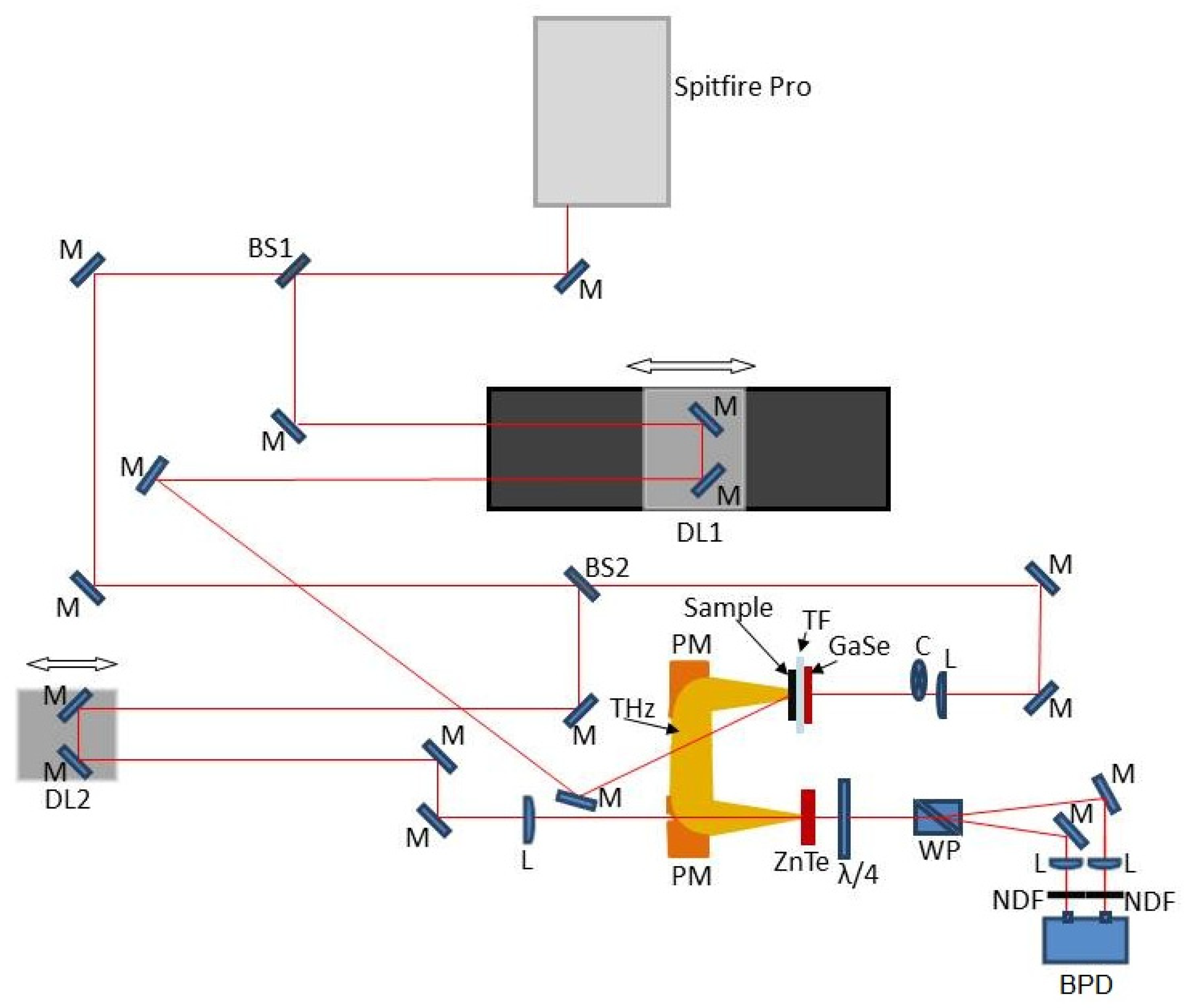
The problem of creating reliable contactless methods for controlling the semiconductor material properties is topical. One of the most promising methods for determining the nonequilibrium charge carrier lifetime is the pump–probe technique, in which, after the excitation of a nonequilibrium charge carrier concentration in a sample by a short, high-intensity laser pulse, a transmission or reflection is sensed by optical or terahertz radiation with certain time delays [8,9,10]. The time resolution of the method may be less than 100 fs. In view of the complexity of the processes occurring in semiconductors when they are photoexcited by short laser pulses, the interpretation and analysis of optical pump–terahertz probe (OPTP) spectroscopy data are still challenging. On the one hand, this method allows the direct sensing of the free charge carrier concentration in semiconductors. On the other hand, due to the photoexcitation character, the OPTP technique can be considered a reliable tool only for studying the temporal dynamics of fast recombination processes at high injection levels, mainly taking place at a semiconductor surface. In view of the above-mentioned problem, it is of interest to determine the extent to which the OPTP method can be used to determine the bulk charge carrier lifetime in semiconductors such as HR GaAs:Cr. In addition, it is meaningful to reveal the dominant recombination mechanisms at the injection levels occurring at OPTP measurements and to determine whether the corresponding experimental data can be used to determine the lifetimes at moderate injection levels. Studies providing new insights into these issues seem to be of interest.
In the present contribution, SI GaAs:EL2 and HR GaAs:Cr structures are studied by the OPTP method. Both HR GaAs:Cr and SI GaAs:EL2 are appropriate materials for ionizing radiation detectors with long charge carrier lifetimes, at the level of tens and hundreds of nanoseconds [5,6,11]. The EL2 defect states in GaAs are usually associated with AsGa antisites or their complexes with other intrinsic defects [12,13]. These are the midgap donor states [12,13]. When the EL2 defect concentration is higher than the concentration of shallow acceptors, while the concentration of shallow acceptors is higher than the concentration of shallow donors in GaAs, the complete compensation of shallow defect states can be reached. This results in a semi-insulating material with a 1.5–3 ns electron lifetime. An alternative approach is doping of n-GaAs with Cr, which is used to achieve the shallow defect state compensation. The Cr-related states are midgap acceptors [4,14]. The chromium compensation technology allows the fabrication of HR GaAs:Cr with a 25–80 ns electron lifetime [6]. Despite the fact that HR GaAs:Cr was successfully used to create ionizing radiation detectors demanded at nuclear physics research centers [15], the mechanisms responsible for the increase in charge carrier lifetime with the introduction of chromium need further investigation. To the best of our knowledge, OPTP spectroscopy has not previously been used to study GaAs:Cr. Nevertheless, the relaxation dynamics of charge carriers in GaAs:Cr were studied by measuring the photoluminescence decay, stationary photoconductivity and photoelectromagnetic effect [16,17]. In these studies, 60–600 ns [16] and 0.5–5 ns [17] lifetimes for electrons were obtained at relatively low injection levels. The values obtained in [16] are in good agreement with the data obtained from the measurements of charge collection efficiency (approximately 80 ns [4]). The results of Ref. [17] are better correlated with the OPTP data obtained for SI-GaAs [9]. As can be seen, there are considerable differences in the charge carrier lifetime values in GaAs obtained by OPTP and by the measurements of photoconductivity decay or charge collection efficiency. This can be attributed to the strong influence of surface states and high injection levels at pump–probe measurements, compared to the two latter methods. To reveal the influence of surface states, in the present study, HR GaAs:Cr and SI GaAs:EL2 wafers with chemically and mechanically treated surfaces were additionally studied by OPTP. The charge carrier lifetimes and contributions from different recombination mechanisms at different injection levels were determined and analyzed for HR GaAs:Cr and SI GaAs:EL2 samples.

2. Experimental and Calculation Details

2.1. Sample Preparation

In the present work, HR GaAs:Cr and SI GaAs:EL2 wafers were studied. The wafers were 450 μm thick. The initial GaAs ingots were purchased from JSC Giredmet, Moscow, Russia. Chromium was introduced by the high-temperature diffusion method. The obtained HR GaAs:Cr had a resistivity of at least 500 MΩ·cm and electron mobility of 4000 cm2/V·s [18]. The SI GaAs:EL2 ingot was purchased from Freiberger Compound Materials GmbH, Freiberg, Germany.
In order to check the influence of surface recombination on the observed charge carrier lifetime, the HR GaAs:Cr and SI GaAs:EL2 wafers were first subjected to the following chemical and mechanical treatments. The first series of samples was mechanically ground on grinding powders with a grain size of 10 μm. This was done to introduce the developed surface defects. The second series of samples was etched in a sulfuric acid etchant (H2O:H2O2:H2SO4 1:1:3) for 1 min at 60 °C. The third series of samples was oxidized. The oxidation was carried out in two ways: oxidation in oxygen plasma for 2 min on a Plasmalab80Plus (Oxford Instruments, Abingdon-on-Thames, UK) setup and oxidation in running water until a visible oxide film appeared on the surface (exposure time was approximately 7 h). The fourth series of samples was covered by a SiO2 film. The 20 nm thick SiO2 film deposition was carried out by magnetron sputtering.

2.2. Optical Pump–Terahertz Probe Setup

The charge carrier relaxation dynamics in the samples were measured by the OPTP method. As is known, this method is based on probing the changes in the terahertz transmittance or reflection of a sample by sending a terahertz pulse onto the sample with various time delays in reference to the short optical pulse, which induces the photogeneration of free charge carriers. The probing possibility is due to the strong absorption of terahertz radiation by free charge carriers.
The schematic view of the experimental setup is shown in Figure 1. For the sample photoexcitation, generation and detection of terahertz pulses, a Spitfire Pro XP regenerative amplifier (Spectra-Physics, Milpitas, CA, USA), which generated pulses with the duration of 35 fs, with energy up to 3.5 mJ at the central wavelength of 791 nm, was used. As can be seen in Figure 1, the laser pulse from the source, passing through the beam splitting plate (BS1), was divided into two pulses of approximately equal power. One of them, passing the delay line DL1, was used for the sample’s photoexcitation. The second one was divided by another beam splitter (BS2). The more intense pulse (97% of power) extracted at BS2 passed through a SR-541 chopper (Standford Research, Sunnyvale, CA, USA) and was focused onto a GaSe crystal to generate a terahertz pulse by optical rectification [19,20]. Another pulse (3% of power) was directed to the delay line DL2 and then to a ZnTe electro-optical crystal for terahertz pulse detection. With the help of DL2, the simultaneity of the probing optical pulse’s arrival and the maximum terahertz pulse field strength (the main maximum) transmitted through the sample at the ZnTe crystal were established. The signal from the balanced photodetector (BPD), Nirvana Model 2007 (New Focus, Milpitas, CA, USA), was registered by a lock-in amplifier, the SR-830 (Standford Research, Sunnyvale, CA, USA). The length of the DL1 delay line allowed us to obtain a maximum delay of around 4 ns. The 1D terahertz transmittance scans were made (by DL1), i.e., the temporal profiles of the terahertz pulses were not recorded in the experiment and only changes in the terahertz pulse field strength at the main maximum were registered. It was checked that the 2D scans did not give any experimental data important for the present study.

2.3. Experimental Data Analysis

To calculate the nonequilibrium charge carrier concentration using the obtained relative differential transmission ΔT/T0 values, the following formula was used [9]:
Δ n ( t ) = N + 1 Z 0 e δ μ ( 1 1 | Δ T T 0 | 1 ) ,
where N = 3.4 is the refractive index of GaAs in the terahertz frequency range, Z0 = 377 Ω is the free space impedance, δ is the penetration depth of laser radiation (taken to be 1 μm for GaAs), μ is the carrier mobility and T0 is the sample terahertz transmittance in the absence of photoexcitation. In the calculations, the possible charge carrier mobility dependence on the temperature or injection level was neglected. Experimental dependences Δn (t) are often analyzed with the assumption that a single recombination mechanism prevails and the charge carrier lifetime is independent of the injection level. In this case, the obtained data can be approximated by the formula
Δ n ( t ) = Δ n 0 exp ( t / τ ) ,
where Δn0 is the initial concentration of nonequilibrium charge carriers, and τ is the charge carrier lifetime. In the present study, it was found that the observed experimental dependences Δn(t) were only roughly approximated by expression (2).
In order to account for the charge carrier lifetime’s dependence on the injection level and to distinguish the contributions from different recombination mechanisms, the following equation was used [9,21]:
1 n ( t ) d n ( t ) d t = 1 τ eff = a + b n ( t ) + c n 2 ( t ) ,
where τeff is the effective charge carrier lifetime, the a coefficient is responsible for the influence of surface and bulk Shockley–Read–Hall recombination, the b coefficient is associated with the effect of interband radiative transitions and Auger recombination through trap levels and the c coefficient is responsible for the interband Auger recombination effect. The experimental data were approximated by the expression
t = d 1 2 a ln ( n 2 a + b n + c n 2 ) + b 2 a b 2 4 a c ln ( b + 2 c n b 2 4 a c b + 2 c n + b 2 4 a c ) .
This expression is the solution of Equation (3) assuming that b2 > 4ac and after swapping the dependent and independent variables. The experimental dependences Δn(t) were plotted in t-n coordinates and numerically fitted by expression (4).

3. Experimental Results

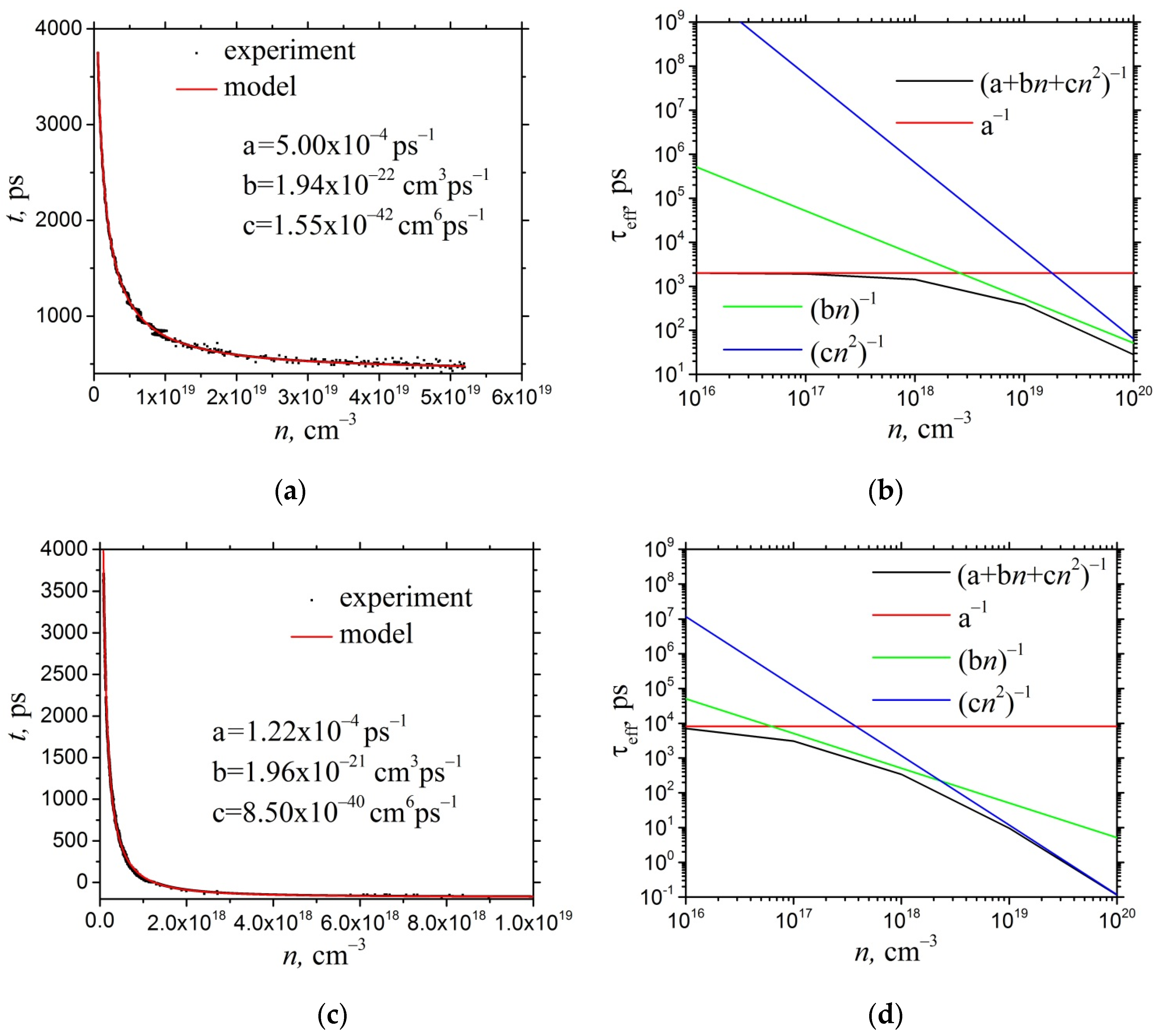
The OPTP experimental data for HR GaAs:Cr shown in Figure 2 indicate that expression (4) allows a rather smooth experimental data approximation. This could not be reached using the approximation by expression (2). The experimental and model dependences of the nonequilibrium charge carrier concentration are shown in Figure 2a, while the calculated effective charge carrier lifetime dependence with the resolution into contributions from different recombination mechanisms for the HR GaAs:Cr sample at the photoexcitation power of 260 mW are given in Figure 2b. The values of coefficients a, b and c obtained as a result of the approximation (Figure 2a) were used to obtain the curves shown in Figure 2b. In Figure 2b, the black curve represents the dependence τeff (n) according to Equation (3). The red curve represents the lifetime if it was determined only by the surface and bulk Shockley–Read–Hall recombination (values b = c = 0 were substituted into Equation (3)). Similarly, the green and blue curves describe the contributions of radiative recombination together with the Auger recombination via traps (at a = c = 0 substituted to (3)) and interband Auger recombination (at a = b = 0 substituted to (3)). As seen in Figure 2b, at nonequilibrium charge carrier concentration levels above 3 × 1018 cm−3, the Auger recombination mechanisms predominate in GaAs:Cr. At the injection levels of 5 × 1017 cm−3 and lower, the lifetime is determined almost exclusively by the bulk and surface Shockley–Read–Hall recombination and it amounts to approximately 2 ns.
The measurements of the same sample were performed at a different photoexcitation pulse power. This was done to check how the range of nonequilbrum charge carrier concentration, at which the experimental data were measured, influences the approximation results and the fitting parameter values. As expected, the obtained dependences show that the nonequilibrium charge carrier lifetime in the limit of low photoexcitation injection levels is determined by the SRH recombination and is 1.4–2 ns for the measurements taken at different photoexcitation power levels (different by one order of magnitude; Figures S1a,b and S2a,b in Supplementary Materials). Thus, the obtained deviation of the extracted a parameter values is not too large. Comparatively, the b parameter values decrease with the photoexcitation power increase from 20 to 260 mW. As it appears, more accurate values for the coefficient b are obtained in the case of measurements with a large photoexcitation level, when the contribution to the total recombination rate from the trap-assisted Auger recombination is larger. The Auger band-to-band recombination coefficient c can be determined only with a large error, since the reachable injection levels are insufficient for this mechanism to dominate in the recombination process. As can be seen in Figure 2, the predominant contribution from the band-to-band Auger recombination occurs at injection levels that were not reached in the experiment.
Further measurements were performed on the samples after chemical and mechanical surface treatments. The results of the measurements and the data analysis for HR GaAs:Cr samples after SiO2 film deposition on the surface, oxidization in oxygen plasma and etching in sulfuric acid solution are presented in Figures S2–S4 in the Supplementary Materials. As was established for the HR GaAs:Cr sample, the deposition of a 20 nm thick SiO2 film, etching in a sulfuric acid solution and plasma oxidation did not lead to a lifetime increase. The values of coefficients a and b also did not change considerably. The observed deviation in c coefficient was probably induced by the insufficiently wide range of experimental data to determine them more precisely.
The mechanical grinding of the HR GaAs:Cr sample surface led to an increase in the charge carrier lifetime in HR GaAs:Cr samples (Figure 2c,d) in the limit of low injection levels. This can be attributed to the filling of SRH recombination centers as a result of the electron redistribution from the created surface defect states. However, at the injection level of 1018 cm−3, the charge carrier lifetime was somewhat reduced to 700–800 ps, which is slightly lower than that of the initial sample. This could also be associated with the generated defect states and Auger recombination with their participation. The role of Auger recombination is predominant at an injection level of ~1017 cm−3 and higher.
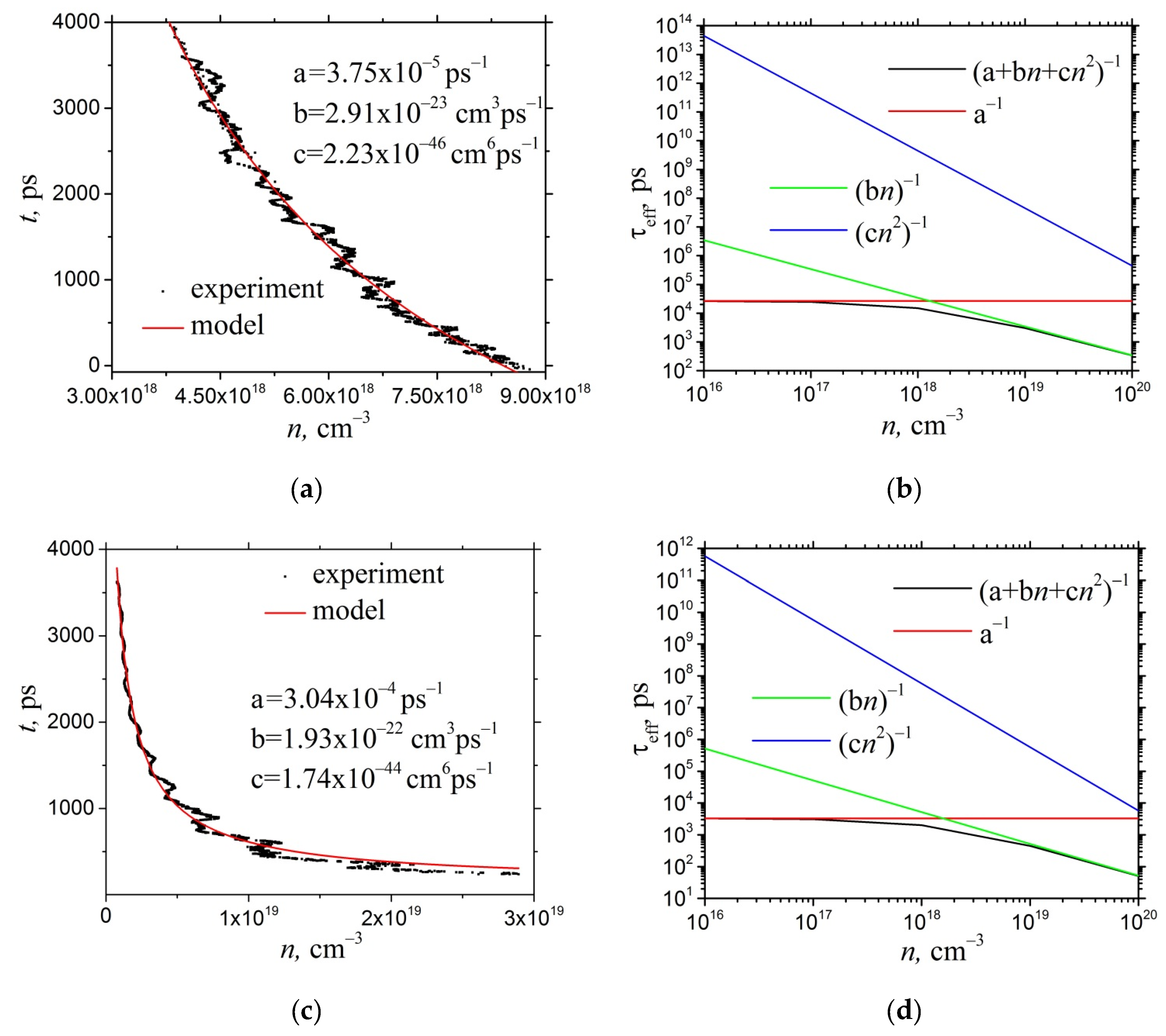
SI GaAs:EL2 samples were studied similarly. For the reference SI GaAs:EL2 sample, the maximum charge carrier lifetime, due to the SRH recombination (25 ns), was determined (Figure 3). The obtained Auger recombination coefficients b and c were significantly lower than the values obtained for other samples. In this case, the mechanical surface grinding led to an increase in surface and SRH recombination (Figure 3c,d). Therefore, it can be supposed that the mechanical treatment generated the defect states, which, in some way, reduced the active SRH recombination center concentration.
The SI GaAs:EL2 samples’ surface oxidation also led to an increase in the surface and SRH recombination rate (Figure S5 in Supplementary Materials).

4. Discussion

The obtained results show that the OPTP technique usually yields higher charge carrier lifetime values compared to the values deduced from the charge collection efficiency measurements. This is due to the higher injection levels and the increased role of Auger recombination in OPTP measurements. The lifetime values obtained using the model accounting for the contribution of different recombination mechanisms and extrapolating the results to the low injection limit amounted to 1–3 ns for HR GaAs:Cr. These injection levels and the corresponding lifetimes are more consistent with the carrier lifetimes and injection levels occurring in HR GaAs:Cr-based ionizing radiation semiconductor detectors.
The OPTP measurements at different photoexcitation power values show that the results are still sensitive to the range of injection levels, especially for the Auger and radiative recombination contributions to the charge carrier lifetime. On the other hand, the SRH recombination rate values are less sensitive to the injection level and can be robustly determined from the OPTP experiments. The charge carrier lifetimes determined by the SRH recombination are important for the HR GaAs:Cr-based X-ray sensor operation. For proper bulk charge carrier lifetime extraction and exclusion of the influence of surface recombination, measurements on samples of different thicknesses would be helpful. However, the measurements performed for the HR GaAs:Cr samples with various surface treatments show that the contribution from the SRH surface is not too large.
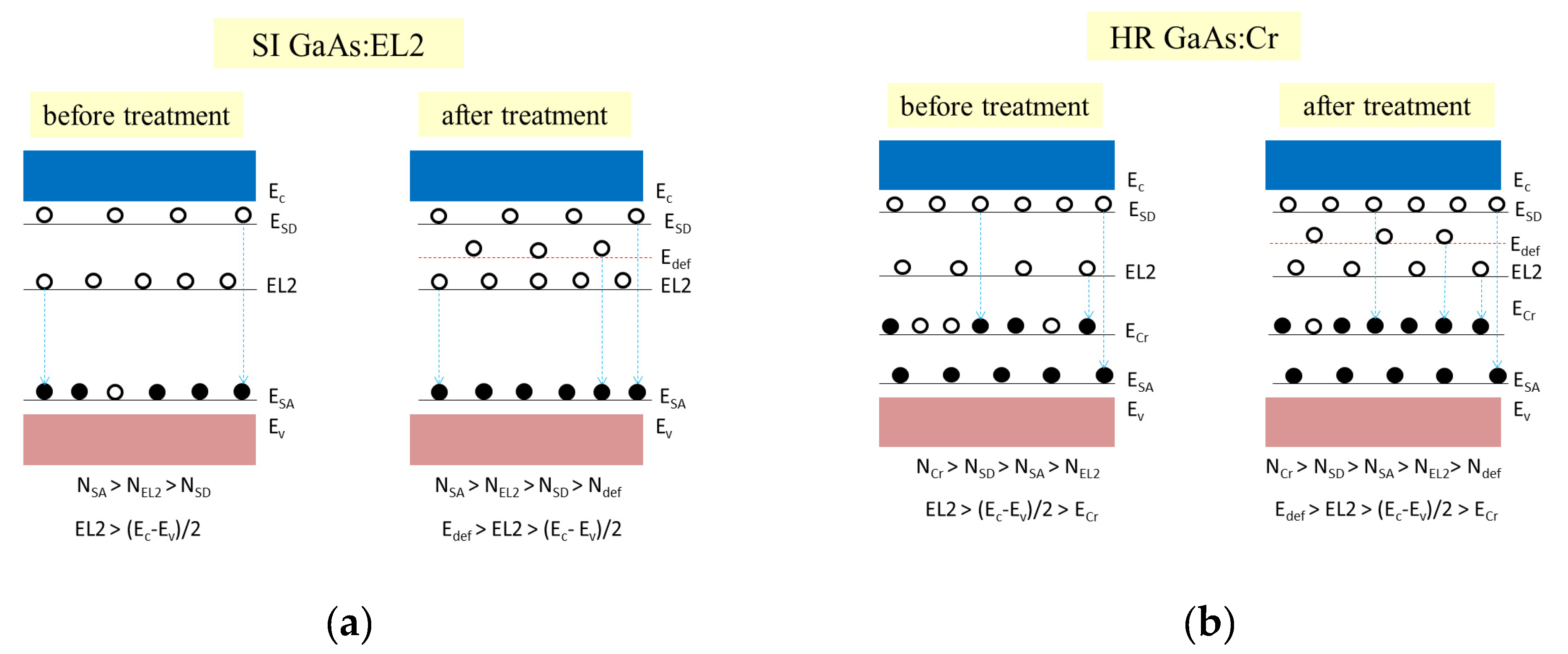
The different influences of surface grinding on the charge carrier lifetimes in SI GaAs:EL2 and HR GaAs:Cr samples could be explained with the use of simple energy diagrams assuming that grinding and subsequent surface reconstruction led to the appearance of additional surface donor-like defect levels in the upper half of the band gap (Figure 4). The formation of such levels was found in Ref. [22] by DFT calculations. In the SI GaAs:EL2 sample, these defect states increased the compensation level, slightly increasing the concentration of active hole traps, but the concentration of SRH recombination centers increased, leading to a charge carrier lifetime reduction (Figure 4a). In the HR GaAs:Cr sample, the defect states increased the filling of the Cr-related acceptor states, reducing the SRH recombination rate, and could also act as deep traps for charge carriers, both increasing the charge carrier lifetime.
As a result of the performed experiments, the time dynamics of the nonequilibrium charge carrier relaxation processes in SI GaAs:EL2 and HR GaAs:Cr semiconductor crystals were studied using the OPTP method. The obtained experimental data were analyzed within the model, taking into account the Shockley–Read–Hall surface and bulk recombination, radiative recombination, band-to-band and trap-assisted Auger recombination. It was found that, at the nonequilibrium charge carrier concentration levels arising in the measurements, with the sample excitation by radiation with a pulse duration of 35 fs, and the pulse energy of 0.26 mJ at the central wavelength of 791 nm, the Auger recombination mechanisms have a significant effect, which leads to the relaxation of the nonequilibrium carrier concentration in HR GaAs:Cr semiconductor crystals during the characteristic times of the order of 500 ps or less. The Auger recombination mechanisms provide a dominant contribution to the nonequilibrium charge carrier recombination rate at injection levels above ~(0.5–3)·1018 cm−3. At lower concentrations, the main recombination mechanism is the SRH recombination. For most HR GaAs:Cr samples, the characteristic lifetimes, due to the SRH recombination, are equal to 1.4–2 ns. The obtained Auger recombination coefficients b and c at the level of 2 × 10⁻¹⁰ cm3/s and 1.5 × 10⁻³⁰ cm6/s are in agreement with those obtained earlier for GaAs by measuring the photoluminescence relaxation kinetics [23]. The results indicate that it is possible to use the terahertz pump–probe spectroscopy method for determining the lifetime in GaAs semiconductor crystals intended for the manufacture of devices requiring long nonequilibrium charge carrier lifetimes.
There is experimental evidence that, at high-intensity fluxes and in high-energy beams, the GaAs detector charge collection efficiency is decreased and the rise time is increased. Usually, during the operation of ionizing radiation detectors on SI-GaAs, the injection level is not high, as a single beta-particle having energy of 2 MeV can produce 1 electron–hole pair per energy of 4.2 eV and have an energy loss of 6 MeV/cm [24]. Thus, a single beta-particle having the energy of 2 MeV can produce 166 electron–hole pairs per 1 μm of path. Taking into account the track diameter of the order of few microns, one can calculate the electron concentration ~ 1012–1014 cm−3. For tracking applications—for example, at the Large Hadron Collider or Forward Calorimeter of International Linear Collider (FCAL ILC)—much larger, higher-energy particle fluxes are available, leading to high injection levels and making high-injection-level measurements of charge carrier lifetime very much relevant.

5. Conclusions

The time dynamics of nonequilibrium charge carrier relaxation processes in SI GaAs:EL2 and HR GaAs:Cr were studied by the optical pump–terahertz probe technique. It was found that, at the concentration level of nonequilibrium charge carriers typical of OPTP measurements, Auger recombination mechanisms have a significant effect. The Auger recombination mechanisms make a decisive contribution to the recombination rate of nonequilibrium charge carriers at injection levels above ~(0.5–3)·1018 cm−3 cm−3. At lower carrier concentrations, the SRH recombination prevails. For HR GaAs:Cr samples, the characteristic charge carrier lifetimes, due to the SRH recombination, are approximately 1.4–2 ns. The obtained results indicate the possibility of applying the OPTP technique to the determination of the charge carrier lifetimes in semiconductor crystals intended for the manufacturing of electronic devices working at lower injection levels, compared to those occurring in pump–probe measurements.

Supplementary Materials

The following are available online at https://www.mdpi.com/article/10.3390/photonics8120575/s1, Figure S1. The experimental and fitting (the parameters are given) time dependences of the nonequilibrium charge carrier concentration at the average photoexcitation beam power of 20 mW (a) in HR GaAs:Cr (b) related calculated injection level dependences of efficient charge carrier lifetime with the resolution into contributions from different recombination mechanisms. Figure S2. The experimental and fitting (the parameters are given) time dependences of the nonequilibrium charge carrier concentration (a) in HR GaAs:Cr after SiO2 film deposition (b) related calculated injection level dependences of efficient charge carrier lifetime with the resolution into contributions from different recombination mechanisms. Figure S3. The experimental and fitting (the parameters are given) time dependences of the nonequilibrium charge carrier concentration (a) in HR GaAs:Cr after etching in sulfuric acid solution (b) related calculated injection level dependences of efficient charge carrier lifetime with the resolution into contributions from different recombination mechanisms. Figure S4. The experimental and fitting (the parameters are given) time dependences of the nonequilibrium charge carrier concentration (a) in HR GaAs:Cr after oxidation in oxygen plasma (b) related calculated injection level dependences of efficient charge carrier lifetime with the resolution into contributions from different recombination mechanisms. Figure S5. The experimental and fitting (the parameters are given) time dependences of the nonequilibrium charge carrier concentration (a) in SI GaAs:EL2 after oxidation in running water (b) related calculated injection level dependences of efficient charge carrier lifetime with the resolution into contributions from different recombination mechanisms. Figure S6. The AFM data for HR GaAs:Cr wafers: (a) initial, (b) after etching in sulfuric acid solution and (c) after grinding the surface. The analysis justifying the Equation (3).

Author Contributions

Conceptualization, O.P.T., Y.S.S., S.Y.S. and V.V.A.; methodology, A.V.T. and S.Y.S.; software, S.Y.S.; validation, Y.S.S. and V.V.A.; formal analysis, S.Y.S.; investigation, I.A.K., D.A.K., R.A.R., V.I.V. and S.Y.S.; resources, O.P.T.; data curation, A.V.T. and V.V.A.; writing—original draft preparation, S.Y.S. and V.V.A.; writing—review and editing, S.Y.S. and V.V.A.; visualization, S.Y.S.; supervision, O.P.T.; project administration, S.Y.S. and V.V.A.; funding acquisition, S.Y.S. and V.V.A. All authors have read and agreed to the published version of the manuscript.

Funding

This work was supported by the Ministry of Science and Higher Education of the Russian Federation (project No FWSM-2020-0038). This study was also supported by the Russian Science Foundation (project 21-19-00046).

Institutional Review Board Statement

Not applicable.

Informed Consent Statement

Not applicable.

Conflicts of Interest

The authors declare no conflict of interest

References

  1. Sarkisov, S.Y.; Safiullin, F.D.; Skakunov, M.S.; Tolbanov, O.P.; Tyazhev, A.V.; Nazarov, M.M.; Shkurinov, A.P. Dipole antennas based on SI-GaAs:Cr for generation and detection of terahertz radiation. Russ. Phys. J. 2013, 53, 890–898. [Google Scholar] [CrossRef]
  2. Zhang, W.D.; Middendorf, J.R.; Brown, E.R. Demonstration of a GaAs-based 1550-nm continuous wave photomixer. Appl. Phys. Lett. 2015, 106, 021119. [Google Scholar] [CrossRef]
  3. Deshmukh, P.; Mendez-Aller, M.; Singh, A.; Pal, S.; Prabhu, S.S.; Nanal, V.; Pillay, R.G.; Dohler, G.H.; Preu, S. Continuous wave terahertz radiation from antennas fabricated on C12-irradiated semi-insulating GaAs. Opt. Lett. 2015, 40, 4540–4543. [Google Scholar] [CrossRef] [PubMed]
  4. Budnitskii, D.L.; Novikov, V.A.; Tolbanov, O.P.; Prudaev, I.A. Charge-carrier lifetimes in high-resistance GaAs doped by chromium diffusion. Russ. Phys. J. 2008, 51, 531–535. [Google Scholar] [CrossRef]
  5. Chsherbakov, I.; Kolesnikova, I.; Lozinskaya, A.; Mihaylov, T.; Novikov, V.; Shemeryankina, A.; Tolbanov, O.; Tyazhev, A.; Zarubin, A. GaAs:Cr X-ray sensors noise characteristics investigation by means of amplitude spectrum analysis. J. Instrum. 2018, 13, C01030. [Google Scholar] [CrossRef]
  6. Veale, M.C.; Bell, S.J.; Duarte, D.D.; French, M.J.; Schneider, A.; Seller, P.; Wilson, M.D.; Lozinskaya, A.D.; Novikov, V.A.; Tolbanov, O.P.; et al. Chromium compensated gallium arsenide detectors for X-ray and γ-ray spectroscopic imaging. Nucl. Instrum. Methods Phys. Res. A 2014, 752, 6–14. [Google Scholar] [CrossRef]
  7. Bereznaya, S.A.; Korotchenko, Z.V.; Redkin, R.A.; Sarkisov, S.Y.; Brudnyi, V.N.; Kosobutsky, A.V.; Atuchin, V.V. Terahertz generation from electron- and neutron-irradiated semiconductor crystal surfaces. Infrared Phys. Techn. 2016, 77, 100–103. [Google Scholar] [CrossRef]
  8. Beard, M.C.; Turner, G.M.; Schmuttenmaer, C.A. Transient photoconductivity in GaAs as measured by time-resolved terahertz spectroscopy. Phys. Rev. B 2000, 62, 15764–15777. [Google Scholar] [CrossRef] [Green Version]
  9. Shi, Y.; Zhou, Q.; Zhang, C.; Jin, B. Ultrafast high-field carrier transport in GaAs measured by femtosecond pump-probe terahertz spectroscopy. Appl. Phys. Lett. 2008, 93, 121115. [Google Scholar] [CrossRef]
  10. Afalla, J.; Gonzales, K.C.; Prieto, E.A.; Catindig, G.; Vasquez, J.D.; Husay, H.A.; Tumanguil-Quitoras, M.A.; Muldera, J.; Kitahara, H.; Somintac, A.; et al. Photoconductivity, carrier lifetime and mobility evaluation of GaAs films on Si (100) using optical pump terahertz probe measurements. Semicond. Sci. Technol. 2019, 34, 035031. [Google Scholar] [CrossRef]
  11. McGregor, D.S.; Rojeski, R.A.; Knoll, G.F. Evidence for field enhanced electron capture by EL2 centers in semi-insulating GaAs and the effect on GaAs radiation detectors. J. Appl. Phys. 1995, 75, 121115. [Google Scholar] [CrossRef] [Green Version]
  12. Kaminska, M. EL2 Defect in GaAs. Phys. Scr. 1987, T19, 551–557. [Google Scholar] [CrossRef]
  13. Krause, R.; Saarinen, K.; Hautojärvi, P.; Polity, A.; Gärtner, G.; Corbel, C. Observation of a monovacancy in the metastable state of the EL2 defect in GaAs by positron annihilation. Phys. Rev. Lett. 1990, 65, 3329–3332. [Google Scholar] [CrossRef]
  14. Hennel, A.M. Semi-insulating transition metal-doped III-VI materials. Acta Phys. Pol. A 1991, 79, 15–29. [Google Scholar] [CrossRef]
  15. Boyko, I.; Burian, P.; Campbell, M.; Chelkov, G.; Cherepanova, E.; Di Girolamo, B.; Gongadze, A.; Janecek, J.; Kharchenko, D.; Kruchonak, U.; et al. Measurement of the radiation environment of the ATLAS cavern in 2017–2018 with ATLAS-GaAsPix detectors. J. Instrum. 2021, 16, P01031. [Google Scholar] [CrossRef]
  16. Papastamatiou, M.J.; Papaioannou, G.J. Recombination mechanism and carrier lifetimes of semi-insulating GaAs:Cr. J. Appl. Phys. 1990, 68, 1094–1098. [Google Scholar] [CrossRef]
  17. Li, S.S.; Huang, C.I. Investigation of the recombination and trapping processes of photoinjected carriers in semi-insulating Cr-doped GaAs using PME and PC methods. J. Appl. Phys. 1972, 43, 1757–1761. [Google Scholar] [CrossRef]
  18. Chsherbakov, I.; Chsherbakov, P.; Lozinskaya, A.; Mihaylov, T.; Novikov, V.; Shemeryankina, A.; Tolbanov, O.; Tyazhev, A.; Zarubin, A.; Beloplotov, D.; et al. Response of HR-GaAs:Cr sensors to subnanosecond X-and β-ray pulses. J. Instrum. 2019, 14, C12016. [Google Scholar] [CrossRef]
  19. Bereznaya, S.A.; Korotchenko, Z.V.; Redkin, R.A.; Sarkisov, S.Y.; Tolbanov, O.P.; Trukhin, V.N.; Gorlenko, N.P.; Sarkisov, Y.S.; Atuchin, V.V. Broadband and narrowband terahertz generation and detection in GaSe1−xSx crystals. J. Opt. 2017, 19, 115503. [Google Scholar] [CrossRef]
  20. Redkin, R.A.; Kobtsev, D.A.; Bereznaya, S.A.; Korotchenko, Z.V.; Sarkisov, Y.S.; Mihaylov, T.A.; Sarkisov, S.Y. GaSe crystals with antireflection coatings for terahertz generation. Mater. Res. Express 2019, 6, 126201. [Google Scholar] [CrossRef]
  21. Kolesnikova, I.I.; Kobtsev, D.A.; Redkin, R.A.; Sarkisov, S.Y.; Tolbanov, O.P.; Tyazhev, A.V. The measurement of charge carrier lifetime in SI-GaAs:Cr and EL2-GaAs by pump-probe terahertz spectroscopy. Russ. Phys. J. 2020, 63, 547–553. [Google Scholar] [CrossRef]
  22. Bacuyag, D.; Escaño, M.C.S.; David, M.; Tani, M. First-principles study of structural, electronic, and optical properties of surface defects in GaAs(001)—β2(2x4). AIP Adv. 2018, 8, 065012. [Google Scholar] [CrossRef] [Green Version]
  23. Strauss, U.; Rühle, W.W.; Köhler, K. Auger recombination in intrinsic GaAs. Appl. Phys. Lett. 1993, 62, 55–57. [Google Scholar] [CrossRef]
  24. Available online: https://physics.nist.gov/PhysRefData/Star/Text/method.html (accessed on 10 November 2021).
Figure 1. Scheme of the experimental setup: L—lens; M—mirror; BS1, BS2—beam splitters; DL1, DL2—delay lines; PM—parabolic mirror; TF—teflon filter; λ/4—quarterwave plate; WP—Wollaston prism; NDF—neutral density filter; BPD—balanced photodetector and C—mechanical chopper.
Photonics 08 00575 g001
Figure 2. The experimental and fitting (the parameters are given) time dependences of the nonequilibrium charge carrier concentration at the average photoexcitation beam power of 260 mW (a) in initial HR GaAs:Cr and (c) after grinding the surface; (b,d) related calculated injection level dependences of efficient charge carrier lifetime with the resolution into contributions from different recombination mechanisms.
Photonics 08 00575 g002
Figure 3. The experimental and fitting (the parameters are indicated) time dependences of the nonequilibrium charge carrier concentration (a) in initial SI GaAs:EL2 and (c) after grinding the surface; (b,d) related calculated injection level dependences of efficient charge carrier lifetime with the resolution into contributions from different recombination mechanisms.
Photonics 08 00575 g003
Figure 4. Energy level diagrams of (a) SI GaAs:EL2 and (b) HR GaAs:Cr before and after the mechanical treatment. The transitions at redistribution of electrons on the energy states are shown with arrows.
Photonics 08 00575 g004
Publisher’s Note: MDPI stays neutral with regard to jurisdictional claims in published maps and institutional affiliations.

