1. Introduction
Electro-optic (EO) polymer modulators have an original advantage of small velocity mismatch between radio-frequency (RF) and optical signals, and by employing a traveling-wave modulation electrode, an optical modulator operable above 100 Gbps was demonstrated [
1,
2,
3]. Although research on EO polymers has been conducted for decades, to prove the technology to be useful for practical application, there are issues to be addressed, such as photo-oxidation, bias drift, large insertion loss, and poor thermal stability [
4,
5,
6].
The photo-oxidation problem can be relaxed by using commercial hermetic packaging, which has been widely adopted for commercial optical devices with much reduced cost recently. The bias drift is mainly caused by the field-assisted drift of impurity ions remaining in the EO polymer material during the material synthesis. The impurity ions can be reduced significantly by employing highly advanced impurity-filtering processes during the material preparation step. Furthermore, the bias-point drift is no longer a concern because recent coherent communication replaces the intensity modulators with phase modulators that do not require bias control. The insertion loss due to the material absorption can be reduced by using fluorinated polymers, which reduces the vibrational absorption for the optical communication wavelengths. The thermal stability can be improved by adopting ridged-backbone polymers such as polyimides.
Various studies have been conducted to improve the EO coefficient and thermal stability. Several approaches aimed to increase the glass transition temperature (
Tg) of poly(methyl methacrylate) (PMMA)-based EO polymers and improve the thermal stability of the device, in which the EO coefficient (
r33) was over 100 pm/V and preserved at 105 °C for 2000 h [
7]. A high EO coefficient was achieved by using novel chromophores, showing a maximum
r33 of 290 pm/V, and maintaining 99% of the initial
r33 at 85 °C for 500 h [
8]. High poling and modulation efficiencies were achieved by taking advantage of the highly confined optical mode in the Si slot waveguide [
9]. State-of-the-art Si-slot EO modulators demonstrated 200 Gbps four-level pulse amplitude modulation (PAM-4) modulation with a low voltage–length product (
Vπ·
L) of 0.41 V·mm and total insertion loss of 0.7 dB [
10].
Several studies were conducted using polyimides in EO modulators. An optical modulator with propagation loss of 1.14 dB/cm and
Vπ of 5.4 V was reported, which employed a guest–host-type polymer [
11,
12]. The chromophores in the guest–host EO polymer could be aligned relatively easily, even in low poling fields, and thus, the EO modulator could achieve low
Vπ. However, it was difficult to maintain the poled order of the chromophores at elevated temperatures. Side-chain EO polymers were confirmed to exhibit superior thermal stability compared to guest–host EO polymers [
1,
7,
13]. Another study was conducted with a polyimide backbone sidechain EO polymer; however, the fabricated modulator exhibited high losses because the polyimide backbone exhibited large absorption [
14].
Fluorinated polymers can reduce the loss of optical signals, caused by the C–H vibrational overtone at a wavelength of 1550 nm [
11,
15,
16,
17]. Therefore, fluorinated polyimides have been widely used as a substrate for flexible organic light-emitting diode (OLED) devices owing to their high transparency, good thermal stability, and excellent mechanical and chemical properties [
17]. The EO polymer used in this study is based on a fluorinated polyimide synthesized from 2,2-Bis (3-amino-4-hydroxyphenyl) hexafluoropropane (6FAP) and 4,4′-(hexafluoroisopropylidene)-diphthalic anhydride (6FDA) [
18].
In this work, we demonstrate EO polymer devices by incorporating a fluorinated polyimide sidechain EO polymer. Polarization modulators and Mach–Zehnder (MZ) intensity modulators are fabricated to measure the EO coefficient of the device and analyze the poling efficiency. We confirm that the coplanar electrode can effectively reduce the bias drift and increase the poling efficiency by discarding the voltage drop across the cladding layers.
2. Preparation of Fluorinated Polyimide EO Polymer and Design of Waveguide Devices with Coplanar Electrodes
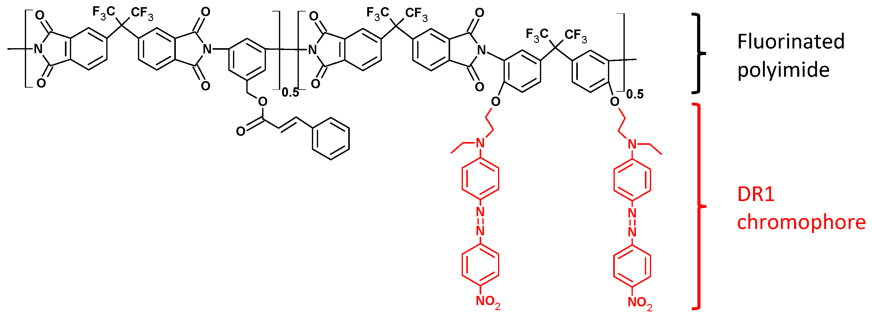
The sidechain EO polymer material with fluorinated polyimide backbone, depicted in
Figure 1, was supplied from Korea Research Institute of Chemical Technology, Daejeon, South Korea [
18]. A hydroxy polyimide was synthesized by the polymerization of the reactants at 150 °C for 3 h. Commercially available DR1 chromophores were selected to obtain the EO property because the chromophores could not be synthesized. The synthesized polymers were post-functionalized by covalently bonding the DR1 chromophores, to yield the EO polymer. The material was supplied in the form of dry red powder and was dissolved in cyclohexanone to produce a 15 wt% solution. The solution was spin-coated on a Si wafer at 700 rpm for 20 s, and baked on a hotplate for 10 min at 80 °C, and for 30 min at 200 °C. The EO coefficient of the thin film, measured by using the reflection method, was 27.7 pm/V at 1310 nm, and the
Tg was exceptionally high as 202 °C. Thermal tests were conducted to confirm that over 90% of the initial
r33 is maintained even after heating at 150 °C for 500 h, proving the superior thermal stability of the material.
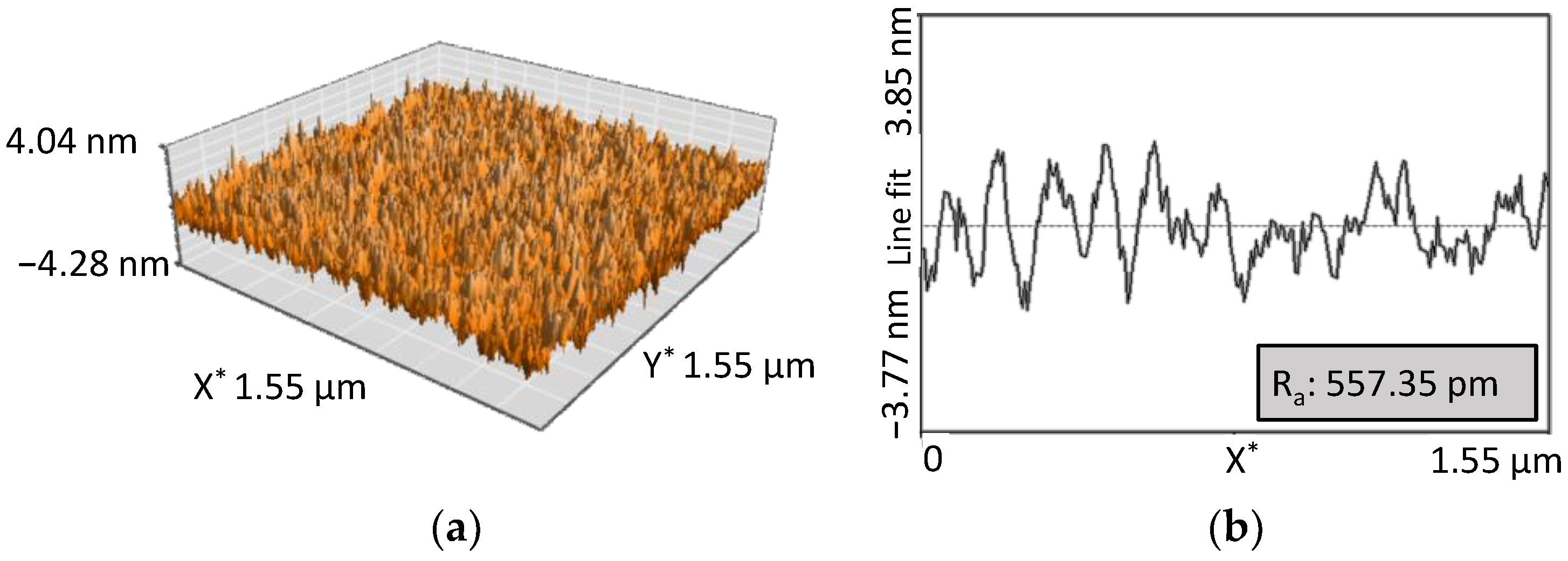
The final thickness of the baked film was 3.7 μm. The film presented excellent surface morphology with a low surface roughness less than 5 nm. The surface roughness of the film was measured using an atomic force microscope, as shown in
Figure 2a. The average surface roughness (
Ra) was measured as 557 pm, as shown in
Figure 2b. The refractive index of the EO polymer film was measured by the prism coupling method with a gadolinium gallium garnet (GGG) prism as 1.6252 and 1.6198 for TE and TM, respectively, for the wavelength of 1550 nm.
The refractive indices of the materials selected for the waveguide device were as follows: 1.445 for SiO2, the lower cladding material; 1.625 for the EO polymer; and 1.501 for NOA74, the upper cladding material. According to the effective index method, rib-structured waveguides with waveguide widths of 4 and 6 μm satisfied the single-mode condition.
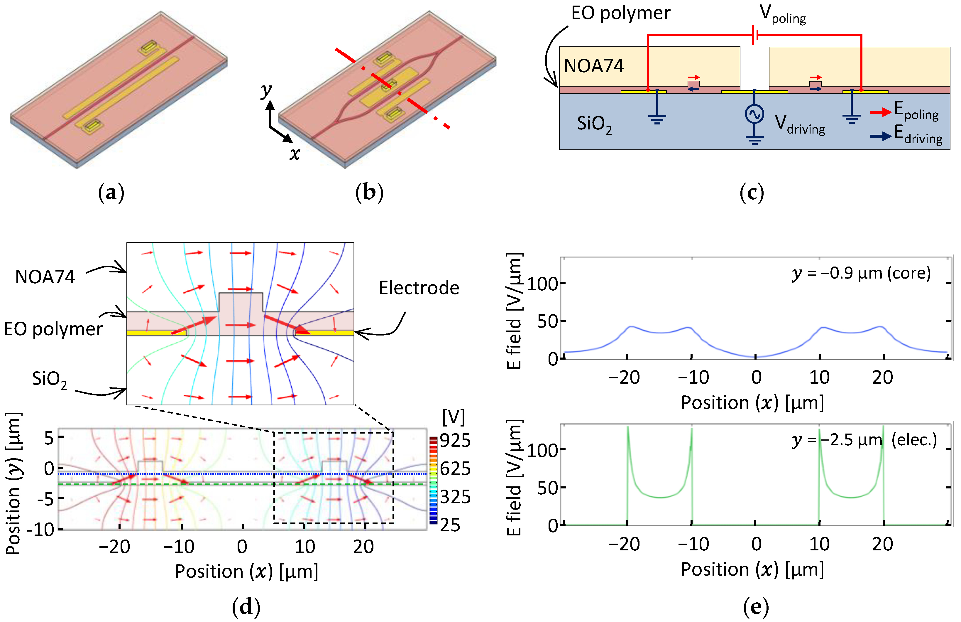
For a straight waveguide, polarization modulators could be produced by placing coplanar electrodes as shown in
Figure 3a. The gap between the electrodes and waveguide had to be close enough to increase the poling and modulation efficiencies until the surface plasmon absorption was not arising. For an input polarization of 45°, both TE and TM modes were excited, and the output polarization depended on the phase retardation between the two polarizations owing to the difference in the EO coefficients of
r33 and
r13. MZ interferometers were designed as shown in
Figure 3b, by placing the coplanar electrodes along the two straight waveguides. The modulation efficiency of the MZ modulator could be doubled by a push–pull operation, where the two waveguides were poled in same direction and operated in opposite directions, as depicted in
Figure 3c.
In the case of vertical poling devices, the electric field crosses the core and cladding materials. A core material doped with chromophores generally exhibits lower resistivity than the cladding material, at an elevated temperature, causing large voltage drops across the cladding layer; thus, the poling field in the core layer would decrease at a high temperature. In coplanar electrode devices, the poling field across the core layer is not affected by the difference in the material resistivity. The poling field distribution of coplanar poling was calculated by the finite element method, assuming that the dielectric constants were uniform throughout the film. The electric potential and field distribution for the applied poling field were calculated as shown in
Figure 3d. The middle electrode was left floating. The poling field at the cores of the two waveguides was parallel to the coplanar electrodes. At vertical positions of the waveguide center and electrode, the electric field intensities along horizontal direction were found as shown in
Figure 3e, where the applied voltage (
V0) was 1 kV and the distance between the edges of the two electrodes (
dg) was 10 μm. The maximum electric field was produced near the edge of the electrode, and that its magnitude decreased further away from the electrode. The magnitude of the effective electric field at the center of the core became 36 V/μm, which was lower than the value expected by uniform field assumption, 50 V/μm (1 kV/20 μm).
3. Fabrication of The EO Polymer Modulator
Prior to the device fabrication, multilayer film coatings were evaluated by coating several materials on top of the annealed EO polymer film, to determine the process compatibility. When a photoresist was coated over the EO polymer film, severe cracking occurred, because of the solvent attack. When low-loss fluorinated polymer ZPU produced by ChemOptics Inc., Daejeon, South Korea, was used as the upper cladding material, cracks appeared after the UV curing of the ZPU polymer film. Finally, UV-curable epoxy NOA74 from Norland Optical Adhesives was selected as the upper cladding material because no damage was found on the EO polymer film even after the UV curing of NOA74.
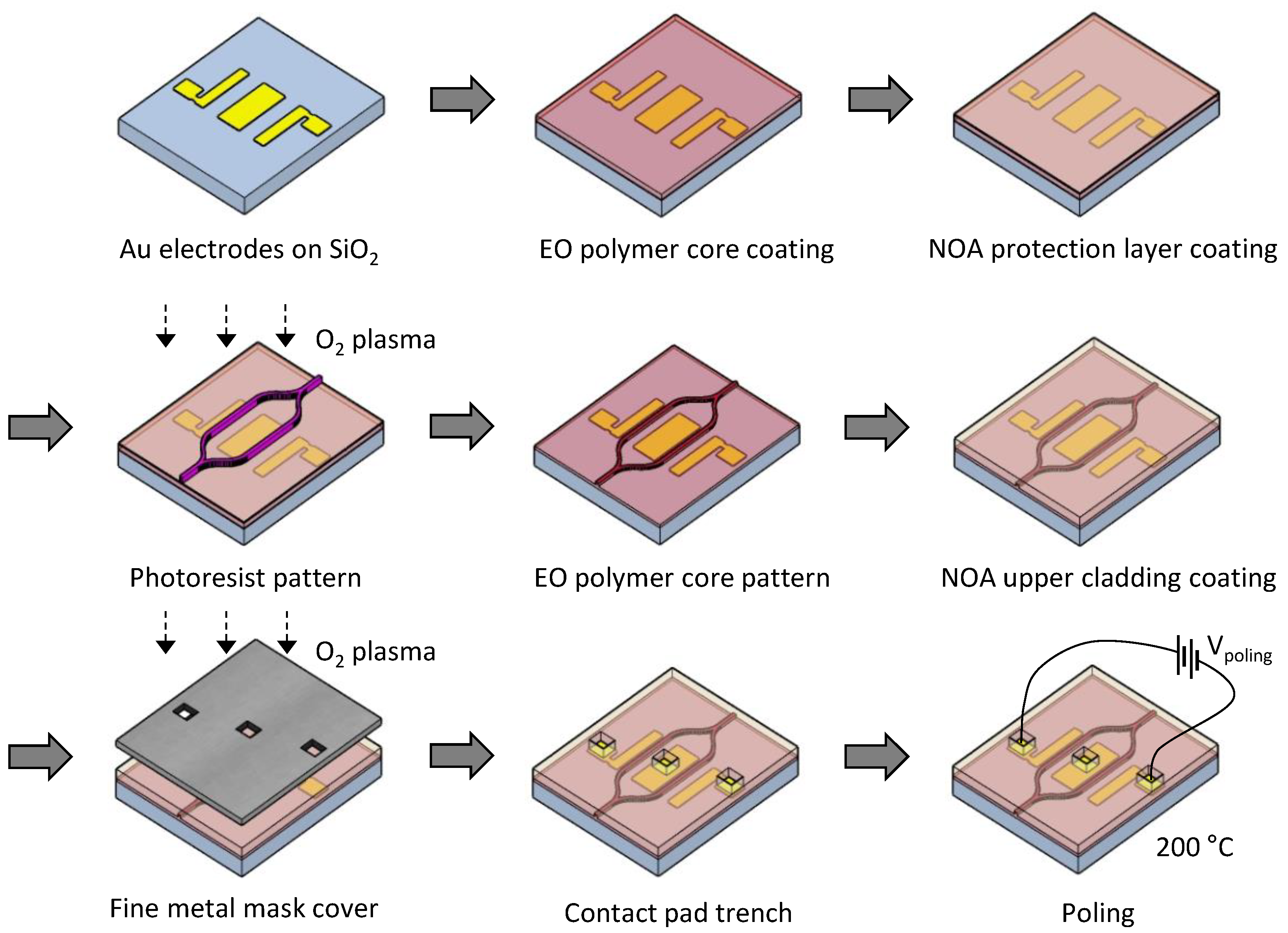
The fabrication process is summarized in
Figure 4. Si substrate with a 14.5 μm oxide layer grown by wet thermal oxidation is used as both the optical cladding and electrical insulating layer. Cr–Au layers of 10–60 nm are deposited to form the electrode. The lift-off process is adopted for electrode fabrication, to prevent the chance of electrical shorts due to the metal residue. The EO polymer is coated on top of the electrode layer producing a 3.7 μm film thickness. Then, NOA74 as a protection layer is covered on the EO polymer with a thickness of 1.0 μm. After the photolithography to define the waveguide pattern, the core layer is etched by 1.2 μm in an oxygen plasma to form a rib waveguide. Then, the upper cladding of 5 μm is formed using NOA74. The metal pads for poling and operation are opened by dry etching the polymer layers through a fine metal mask.
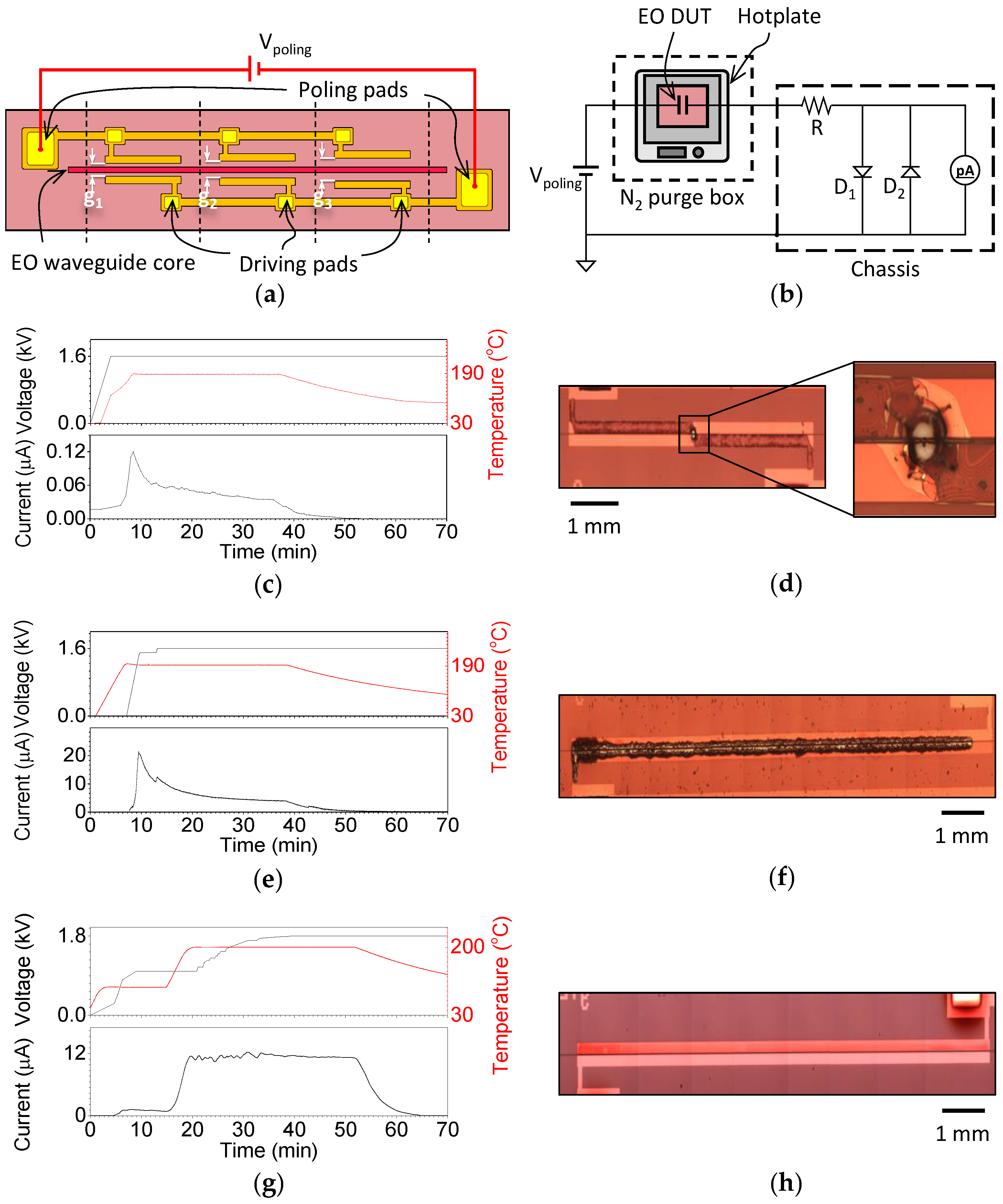
To reduce the burden of experimental work in optimizing the poling process, we designed the electrodes as shown in
Figure 5a. Three pairs of electrodes with different gaps (12, 16, and 20 μm) were connected in parallel to form the same potential difference across them and perform poling simultaneously. When the poling voltage was increased slowly, the device with a narrow electrode gap experienced the highest electric field first and proceeded to breakdown if the voltage was increased beyond a certain extent. Then, we presume that a maximum field before the breakdown was applied to the devices with wider electrode gaps.
In the poling setup shown in
Figure 5b, spring contact probes were used. The pads were covered lightly with silver paste, to ensure contact without damaging the thin metal pads. The sample was poled on a hot plate inside a nitrogen purge chamber to prevent the oxidation of the chromophore molecules at high temperatures and remove the effects of moisture [
4]. The oxygen concentration inside the chamber reached 1.6% after 10 min of N
2 purging. The amount of current flowing through the EO polymer during the poling process was measured using a picoammeter (Keithley 6485). A resistor was placed as a current-limiting load after the DUT and two diodes in opposite directions were connected in parallel with the picoammeter to prevent accidental high currents through the picoammeter. As the temperature increased, the resistance of the EO polymer dropped, causing an increase in the current flow.
In the first few trials of poling, the voltage was increased to a high level first, prior to the temperature elevation, as shown in
Figure 5c. In this case, an early breakdown was observed on the electrode, as shown in
Figure 5d, caused by a defect near the electrode. Electro-optic properties were barely observed in this device. In the second case, the temperature was increased first, then the voltage was raised, as shown in
Figure 5e. An excessive amount of current suddenly flowed because of the rapid voltage increase at the poling temperature, which led to dielectric breakdown, as shown in
Figure 5f.
The poling process was optimized to limit the maximum current flow during the poling, by controlling the temperature and voltage in several steps, as shown in
Figure 5g. At the first step, the voltage was increased gradually up to 1 kV, which was guaranteed as a safe voltage from the previous experiments. By observing the current flow at 200 °C, the voltage was gradually increased to the maximum poling voltage of 1.8 kV, corresponding to an electric field of 100 V/μm. Thus, we were able to avoid breakdown and achieve the highest poling efficiency.
4. Measurement of the Optical Waveguide and MZ Modulator Performance
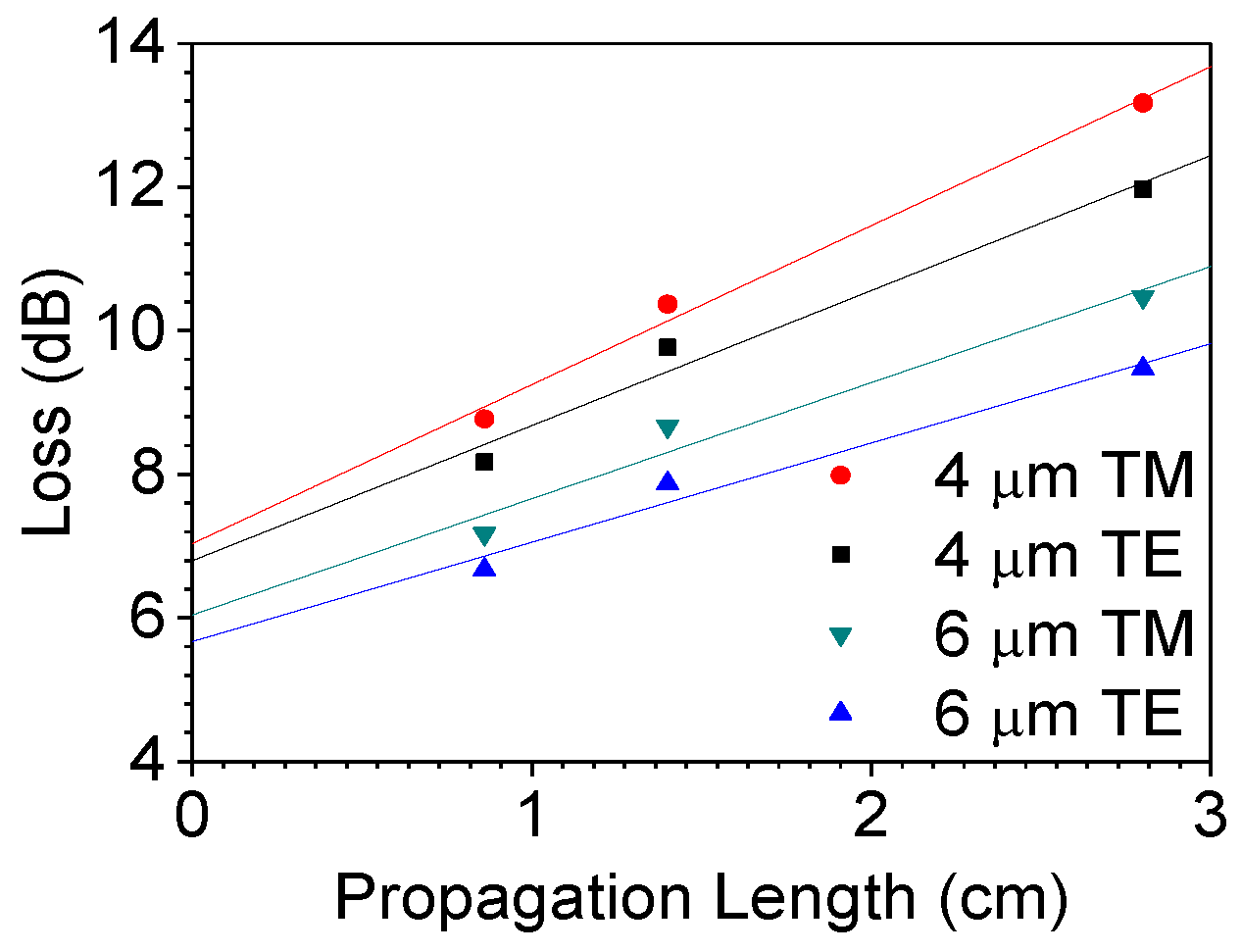
The insertion losses of the devices with different lengths were measured using a 1550 nm distributed feedback (DFB) laser, as shown in
Figure 6. Single-mode fibers were aligned with the device, and a fiber-optic polarization controller was used to adjust the input polarization to TE or TM. The propagation losses of a 4-μm-core waveguide were measured as 1.9 and 2.2 dB/cm for TE and TM, respectively. For a 6-μm-core waveguide, the propagation losses measured for TE and TM polarizations were 1.4 and 1.6 dB/cm, respectively, which indicated that the 6-μm waveguide had better mode confinement. The coupling losses of the 4- and 6-μm waveguides were 3.3 and 2.9 dB/facet, respectively. From comparisons with the measurement results of the unpoled samples, the poling-induced loss was approximately 0.5 dB/cm.
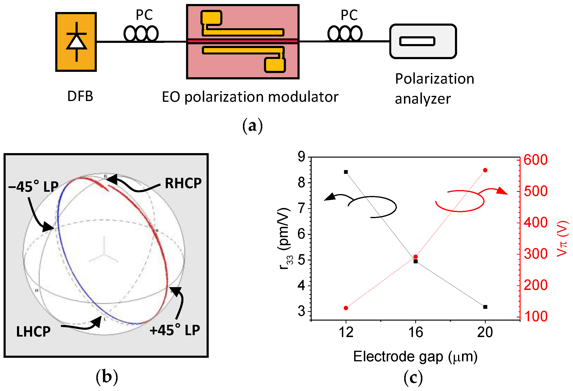
To observe the polarization modulation, caused by the difference between
r13 and
r33 EO coefficients, a straight waveguide modulator was characterized with a 1550 nm DFB source, as shown in
Figure 7a. The length of device was 10 mm with an electrode length of 5 mm. The input polarization was adjusted to +45° linear polarization, and the output polarization was observed using a CCD through a −45° free-space polarizer to confirm the intensity modulation due to the polarization change. Then, the output polarization was monitored using a polarization analyzer (General Photonics, POD-101), and 2π phase retardation was observed between the TE and TM modes, as shown in
Figure 8b. Assuming
r33 ≈ 3
r13,
r33 could be calculated from the measured
Vπ for complete polarization conversion [
19]. For a poling voltage of 1.8 kV, the actual poling field at the center of the waveguide core became 100, 77, and 63 V/μm, corresponding to electrode gaps of 12, 16, and 20 μm, respectively. The 12 μm gap electrode showed a
Vπ of 128 V, and the obtained
r33 value was 8.42 pm/V, as shown in
Figure 7c.
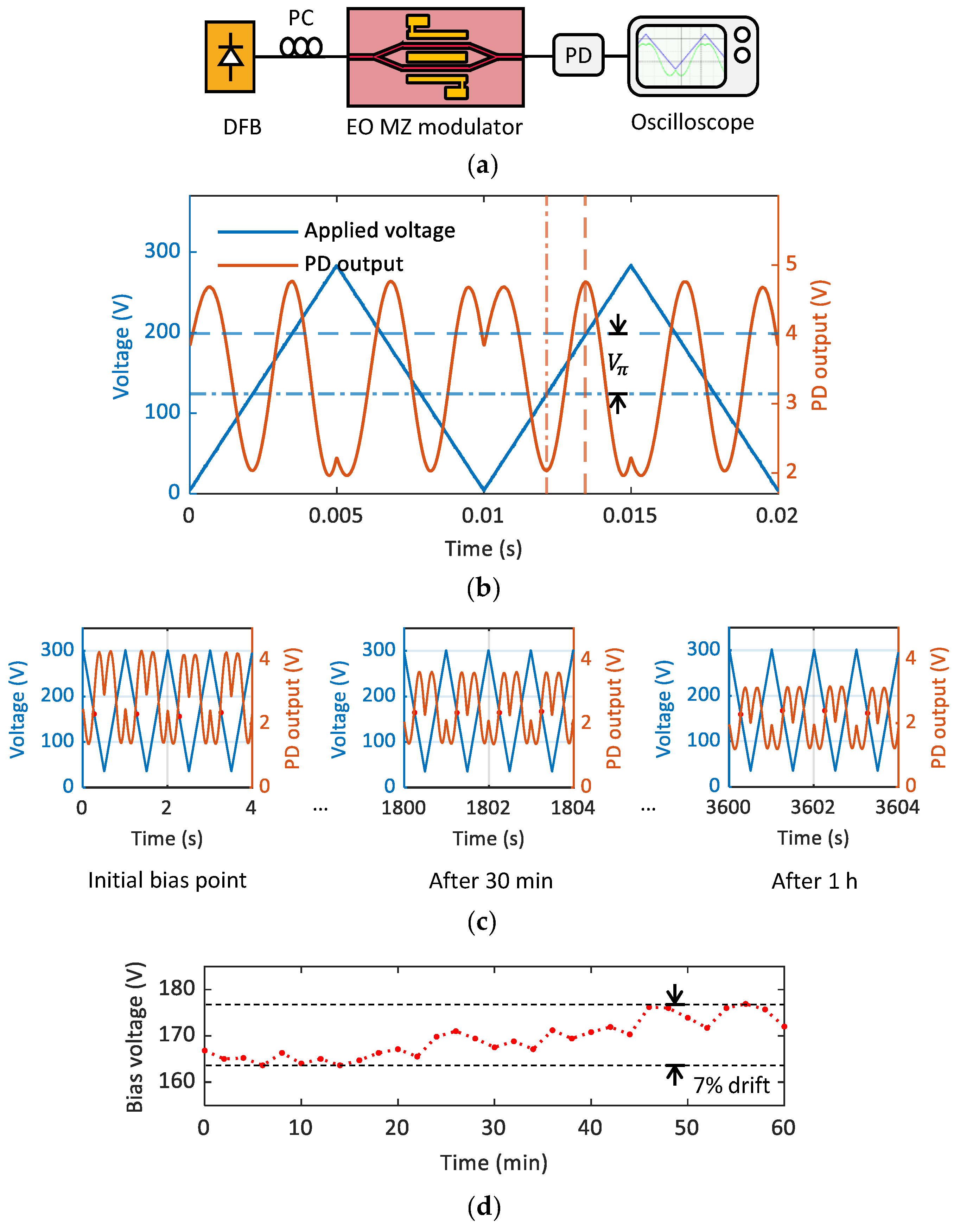
The MZ modulator was characterized using the experimental setup illustrated in
Figure 8a. The length of the device was 20 mm with an electrode length of 5 mm. The
Vπ of 12 μm gap electrodes on each arm was measured as 75 V, as can be seen in
Figure 8b. It was poled with a poling field of 80 V/μm by applying 2.9 kV across the two arms with the middle electrode remaining as floating. The
r33 calculated from the measured
Vπ was 7.22 pm/V. The bias drift of MZ modulator was observed by monitoring the intensity modulation waveform with a bias voltage of 167 V applied for an hour. As shown in
Figure 8c, the waveform changed only slightly in an hour, which indicated that the bias point for quadrature phase difference did not drift significantly. In the case of the ordinary EO polymer device with a vertical field application, the bias voltage was divided proportional to the resistivities of the core and cladding polymers and exhibited a considerably fast drift within a few minutes [
4,
5]. The bias voltage variation measured for an hour was as small as 7%, as shown in
Figure 8d. The amplitude of output waveform was slightly decreased due to the alignment degradation of butt-coupled fibers. For the longer-term measurement of bias stability, in the next step, we will prepare a complete packaged device to improve the optical alignment stability.
5. Conclusions
Based on fluorinated polyimide, a novel EO polymer material was synthesized, and used for the development of an EO polymer modulator with a coplanar electrode, which could provide efficient poling and reduced DC drift. The EO polymer with fluorinated polyimide backbone had the advantages of improved thermal stability and low absorption losses due to the C–H vibration overtone. The poling process was optimized by limiting the maximum current flow during the stepwise voltage increase. An EO coefficient of 8.42 pm/V was obtained from a polarization modulation device at 1550 nm wavelength, which was quite high considering the DR1 chromophore attached to the fluorinated polyimide. The MZ modulator was poled with a lower degree of poling because of the wide electrode gap, and Vπ was measured to be 75 V with a 5-mm-long electrode, in the push–pull operation. From the measurement of the bias-drift effect, we confirmed that the coplanar electrode could provide significant improvement over the conventional vertical poling device.
To improve the performance of the EO polymer waveguide devices by maximizing the poling efficiency, the device fabrication process must be enhanced so as to reduce the electrode gap. The poling field should be increased, and to do so, the device must be fabricated without any defects causing dielectric breakdown. As the commercial DR1 chromophore has a low EO effect, chromophores with high dipole moments and hyperpolarizabilities should be incorporated as sidechains into the fluorinated polyimides. Then, the EO coefficient can be improved, and EO polymer modulators with low loss, high thermal stability, and low Vπ can be achieved based on the coplanar electrodes.
Author Contributions
Conceptualization, M.-C.O. and E.-S.L.; methodology, E.-S.L.; data analysis, E.-S.L., S.-M.K., and M.-C.O.; material preparation, M.-H.Y. and J.-W.K.; writing—original draft preparation, E.-S.L and M.-C.O.; writing—review and editing, E.-S.L and M.-C.O. All authors have read and agreed to the published version of the manuscript.
Funding
This research was supported by National Research Foundation of Korea (NRF) grant funded by the Korea government (MSIP) (2020R1A2C2101562).
Conflicts of Interest
The authors declare no conflict of interest.
References
- Nalwa, H.S. Nonlinear Optics of Organic Molecules and Polymers; CRC Press: Boca Raton, FL, USA, 1997. [Google Scholar]
- Steier, W.H.; Chen, A.; Lee, S.S.; Garner, S.; Zhang, H.; Chuyanov, V.; Dalton, L.R.; Wang, F.; Ren, A.S.; Zhang, C.; et al. Polymer Electro-Optic Devices for Integrated Optics. Chem. Phys. 1999, 245, 1–3. [Google Scholar] [CrossRef]
- Enami, Y.; Seki, A.; Masuda, S.; Joichi, T.; Luo, J.; Jen, A.K.Y. Bandwidth Optimization for Mach-Zehnder Polymer/Sol-Gel Modulators. J. Light. Technol. 2018, 36, 4181–4189. [Google Scholar] [CrossRef]
- Oh, M.C.; Zhang, H.; Zhang, C.; Erlig, H.; Chang, Y.; Tsap, B.; Chang, D.; Szep, A.; Steier, W.H.; Fetterman, H.R.; et al. Recent Advances in Electrooptic Polymer Modulators Incorporating Highly Nonlinear Chromophore. IEEE J. Sel. Top. Quantum Electron. 2001, 7, 826–835. [Google Scholar] [CrossRef]
- Park, H.; Hwang, W.Y.; Kim, J.J. Origin of Direct Current Drift in Electro-Optic Polymer Modulator. Appl. Phys. Lett. 1997, 70, 2796–2798. [Google Scholar] [CrossRef]
- Lee, M.S. Photo-and Thermo-Stabilization of Second-Order Nonlinear Optical Polymers. Ph.D. Thesis, University of Southern California, Los Angeles, CA, USA, 2006. [Google Scholar]
- Miura, H.; Qiu, F.; Spring, A.M.; Kashino, T.; Kikuchi, T.; Ozawa, M.; Nawata, H.; Odoi, K.; Yokoyama, S. High Thermal Stability 40 GHz Electro-Optic Polymer Modulators. Opt. Express 2017, 25, 28643–28649. [Google Scholar] [CrossRef]
- Xu, H.; Liu, F.; Elder, D.L.; Johnson, L.E.; De Coene, Y.; Clays, K.; Robinson, B.H.; Dalton, L.R. Ultrahigh Electro-Optic Coefficients, High Index of Refraction, and Long-Term Stability from Diels-Alder Cross-Linkable Binary Molecular Glasses. Chem. Mater. 2020, 32, 1408–1421. [Google Scholar] [CrossRef]
- Kieninger, C.; Kutuvantavida, Y.; Elder, D.L.; Wolf, S.; Zwickel, H.; Blaicher, M.; Kemal, J.N.; Lauermann, M.; Randel, S.; Freude, W.; et al. Ultra-High Electro-Optic Activity Demonstrated in a Silicon-Organic Hybrid Modulator. Optica 2018, 5, 739–748. [Google Scholar] [CrossRef] [Green Version]
- Kieninger, C.; Fullner, C.; Zwickel, H.; Kutuvantavida, Y.; Kemal, J.N.; Eschenbaum, C.; Elder, D.L.; Dalton, L.R.; Freude, W.; Randel, S.; et al. SOH Mach-Zehnder Modulators for 100 GBd PAM4 Signaling with Sub-1 DB Phase-Shifter Loss. In Proceedings of the Optical Fiber Communications Conference, San Diego, CA, USA, 8–12 March 2020. [Google Scholar] [CrossRef]
- Hubbard, S.F.; Singer, K.D.; Li, F.; Cheng, S.Z.D.; Harris, F.W. Nonlinear Optical Studies of a Fluorinated Poled Polyimide Guest-Host System. Appl. Phys. Lett. 1994, 65, 265–267. [Google Scholar] [CrossRef] [Green Version]
- Tang, J.; Zhang, L.J.; De Wang, L.; Shan, F.; Zhang, T. Low Loss Polymeric Electro-Optic Modulator Based on Disperse Red 1 Doped Fluorinated Polyimide. In Proceedings of the 26th Wireless and Optical Communication Conference, Newark, NJ, USA, 7–8 April 2017. [Google Scholar] [CrossRef]
- Ma, H.; Liu, S.; Luo, J.; Suresh, S.; Liu, L.; Kang, S.H.; Haller, M.; Sassa, T.; Dalton, L.R.; Jen, A.K.Y. Highly Efficient and Thermally Stable Electro-Optical Dendrimers for Photonics. Adv. Funct. Mater. 2002, 12, 565–574. [Google Scholar] [CrossRef]
- Mikerin, S.L.; Plekhanov, A.I.; Simanchuk, A.E.; Yakimanskii, A.V.; Martynenkov, A.A.; Valisheva, N.A. Compact Amplitude Electro-Optic Modulator Based on Chromophore-Containing Polyimides. Optoelectron. Instrum. Data Process. 2018, 54, 385–389. [Google Scholar] [CrossRef]
- Oh, M.C.; Kim, K.J.; Chu, W.S.; Kim, J.W.; Seo, J.K.; Noh, Y.O.; Lee, H.J. Integrated Photonic Devices Incorporating Low-Loss Fluorinated Polymer Materials. Polymers 2011, 3, 975–997. [Google Scholar] [CrossRef] [Green Version]
- Luo, J.; Ma, H.; Haller, M.; Jen, A.K.Y.; Barto, R.R. Large Electro-Optic Activity and Low Optical Loss Derived from a Highly Fluorinated Dendritic Nonlinear Optical Chromophore. Chem. Commun. 2002, 8, 888–889. [Google Scholar] [CrossRef] [PubMed]
- Ando, S. Optical Properties of Fluorinated Polyimides and Their Applications to Optical Components and Waveguide Circuits. J. Photopolym. Sci. Technol. 2004, 17, 219–232. [Google Scholar] [CrossRef] [Green Version]
- Chung, J.; Seo, H.; Lim, J.; Kim, G.; Yi, M.H.; Ka, J.W. A Photo-Functional Electro-Optic Polyimide with Excellent High-Temperature Stability. Dye. Pigment. 2019, 163, 547–552. [Google Scholar] [CrossRef]
- Chen, A.; Murphy, E. Broadband Optical Modulators: Science, Technology, and Applications; CRC Press: Boca Raton, FL, USA, 2016. [Google Scholar]
| Publisher’s Note: MDPI stays neutral with regard to jurisdictional claims in published maps and institutional affiliations. |
© 2020 by the authors. Licensee MDPI, Basel, Switzerland. This article is an open access article distributed under the terms and conditions of the Creative Commons Attribution (CC BY) license (http://creativecommons.org/licenses/by/4.0/).


