Recent Advances in High Speed Photodetectors for eSWIR/MWIR/LWIR Applications


Abstract
:1. Introduction
2. Design Consideration of High-Speed Photodetector
2.1. Cut-Off Wavelength
2.2. Response Speed
3. States-of-the-Art for High Speed Infrared Photodetectors
3.1. For eSWIR Operation
3.2. MWIR Operation
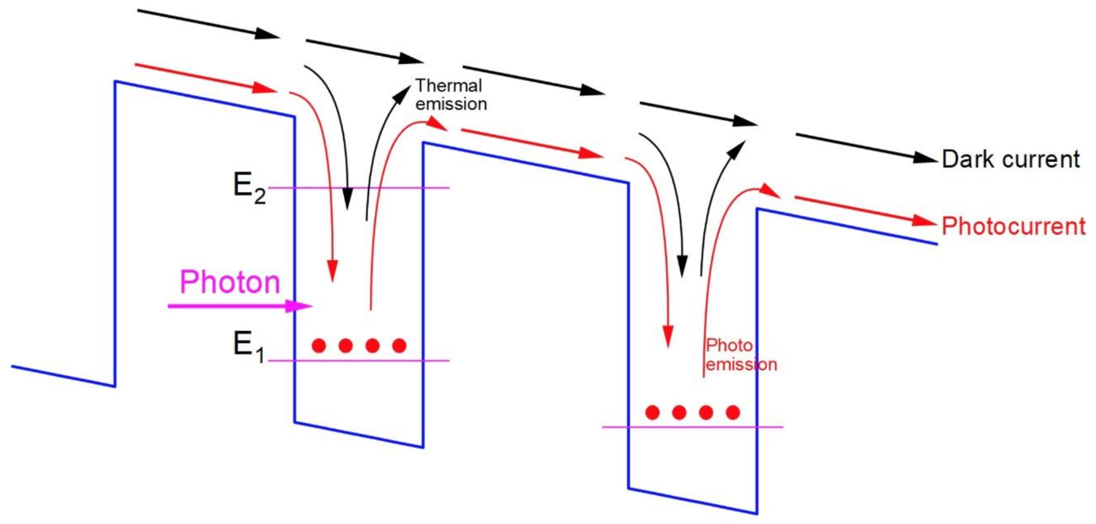
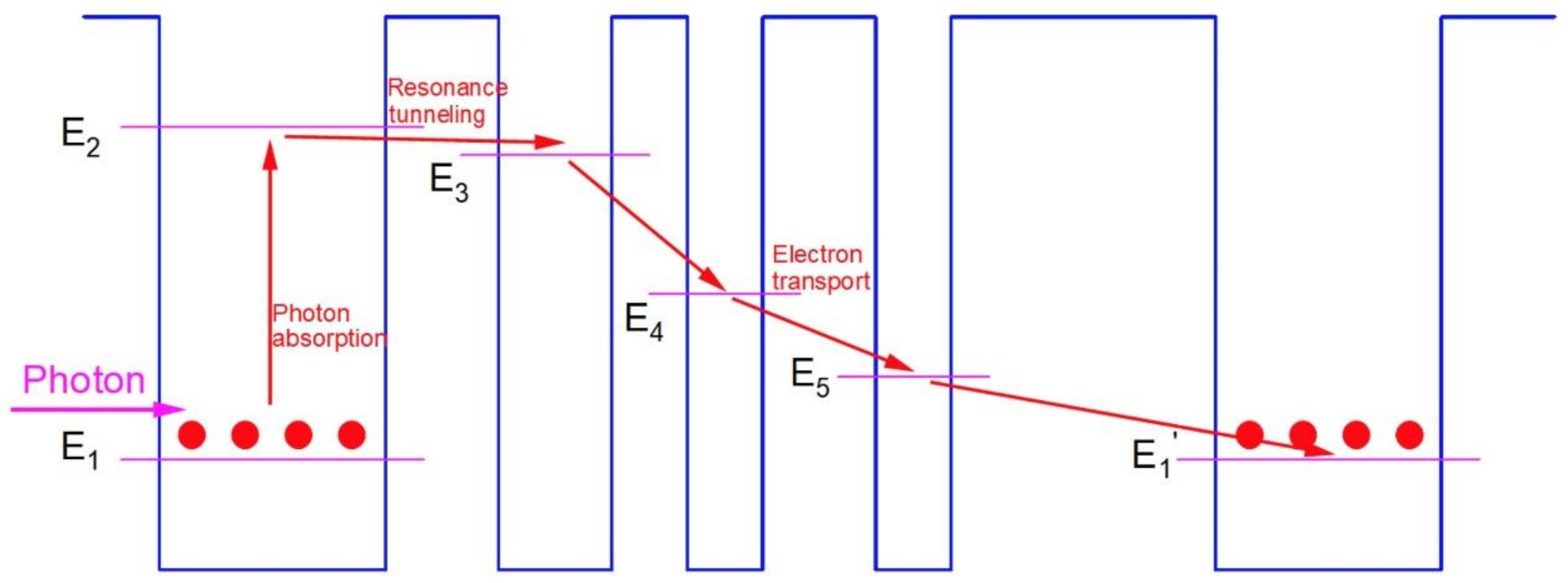
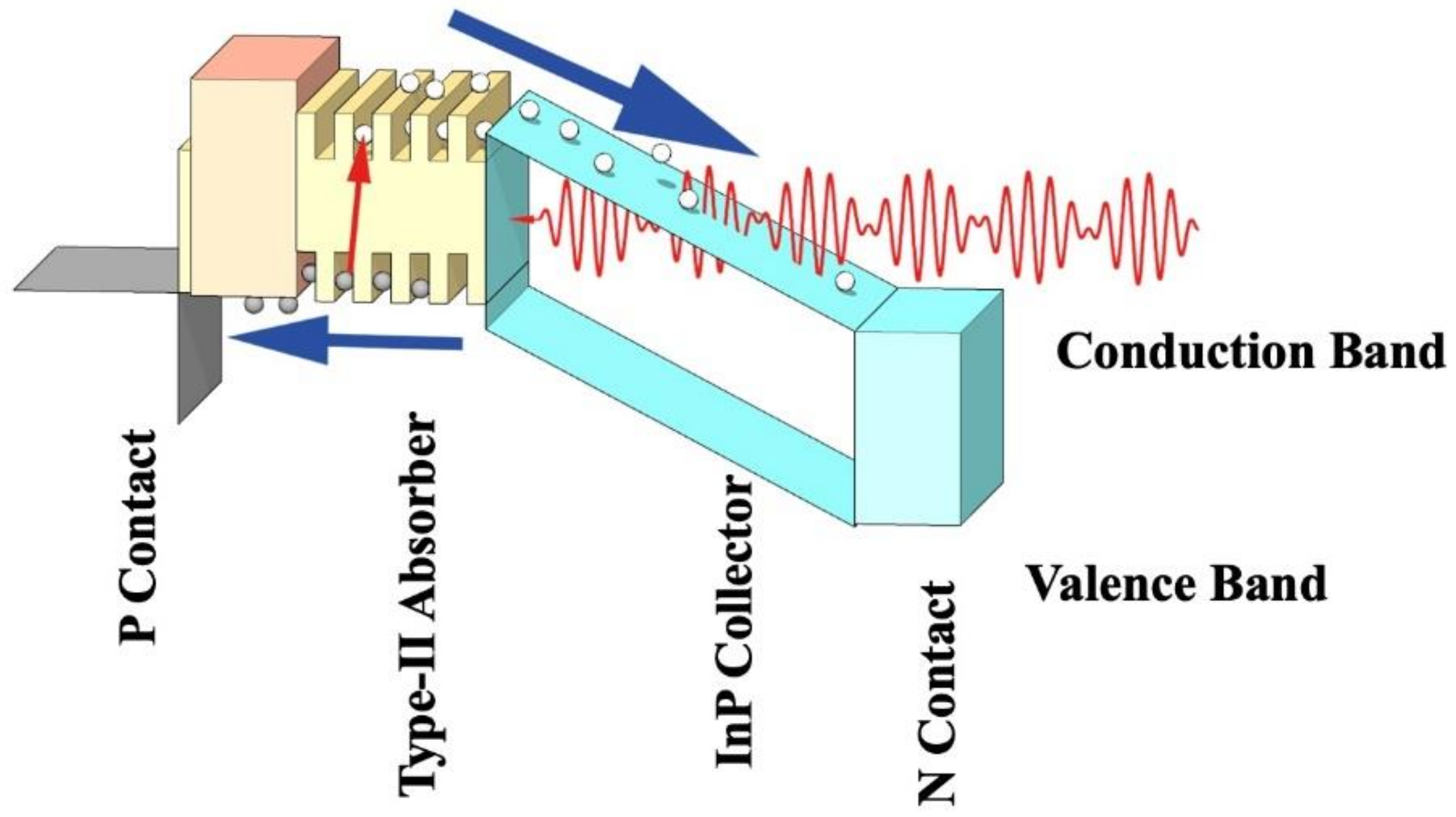
3.3. LWIR Operation
4. Challenges and Perspectives
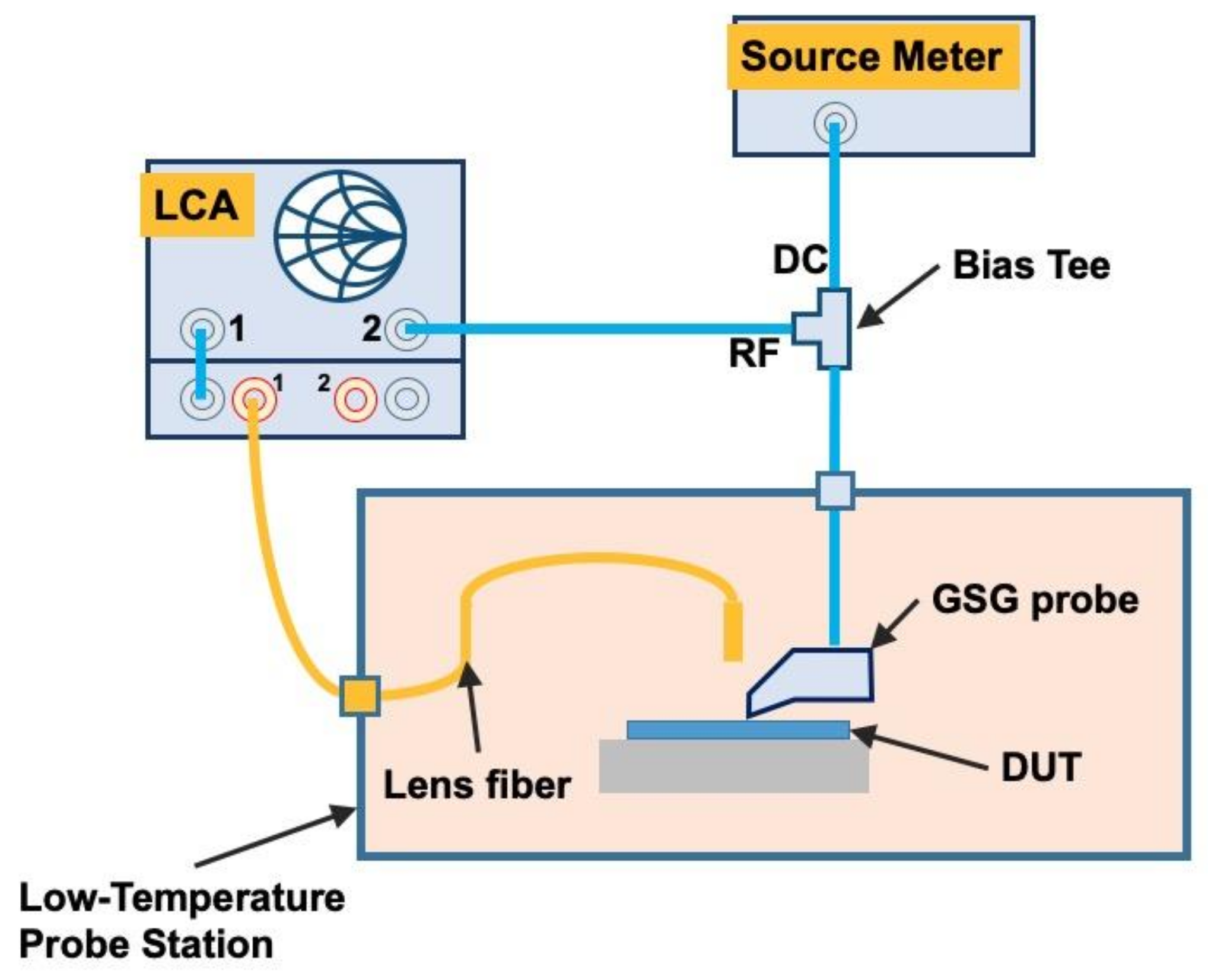
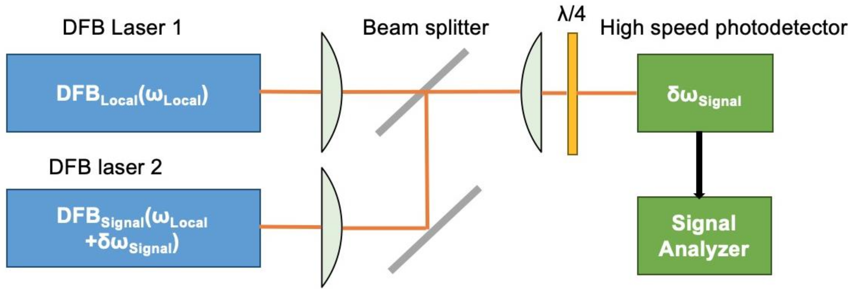
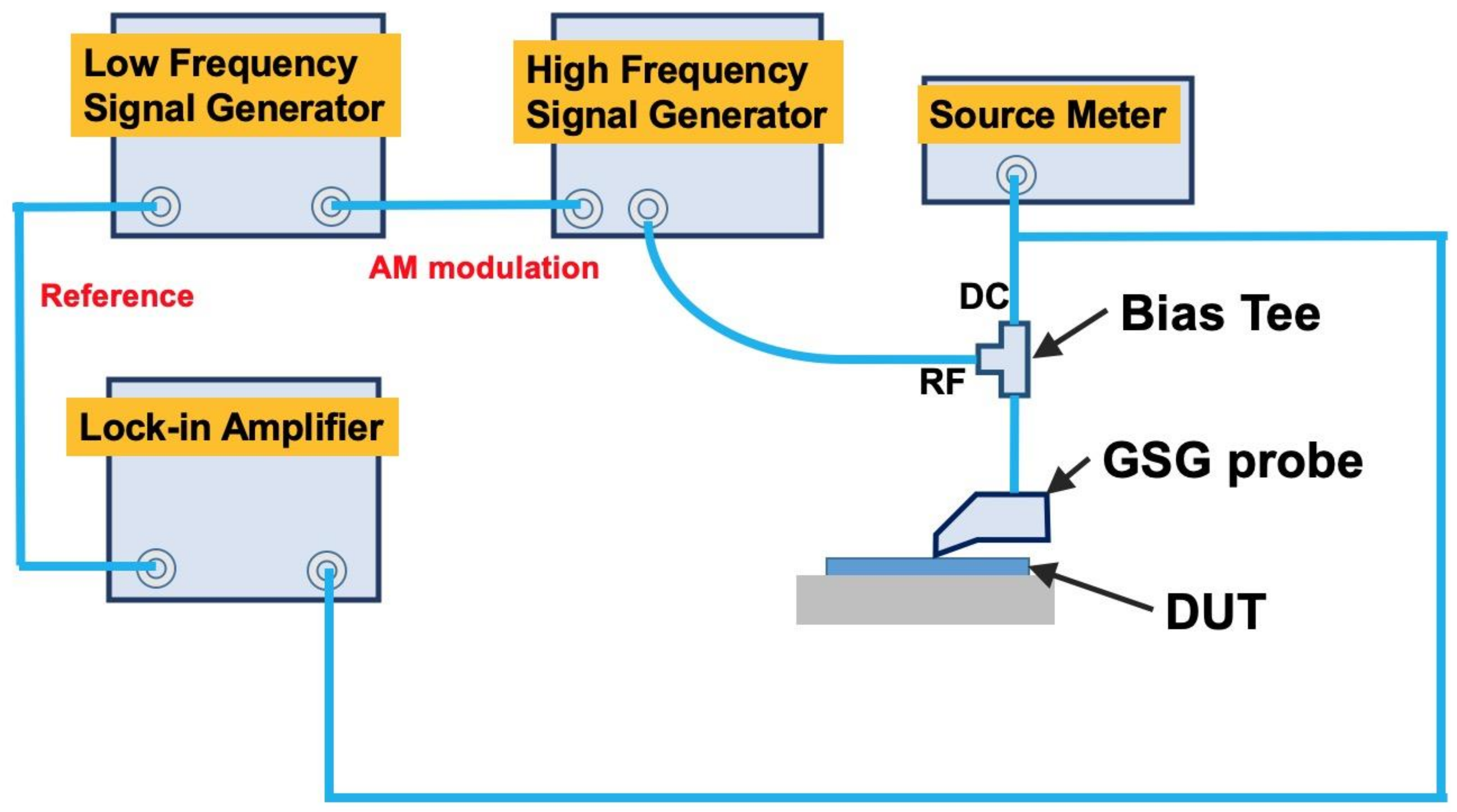
4.1. Bandwidth Characterization
4.2. Design Challenges
4.3. Perspectives
5. Conclusions
Author Contributions
Funding
Conflicts of Interest
References
- Ellis, A.D.; Zhao, J.; Cotter, D. Approaching the Non-Linear Shannon Limit. J. Lightwave Technol. 2010, 28, 423–433. [Google Scholar] [CrossRef] [Green Version]
- Roberts, P.J.; Couny, F.; Sabert, H.; Mangan, B.J.; Williams, D.P.; Farr, L.; Mason, M.W.; Tomlinson, A.; Birks, T.A.; Knight, J.C.A. Ultimate low loss of hollow-core photonic crystal fibres. Opt. Express 2005, 13, 236. [Google Scholar] [CrossRef] [PubMed] [Green Version]
- Li, Z.; Heidt, A.; Simakov, N.; Jung, Y.; Daniel, J.; Alam, S.; Richardson, D. Diode-pumped wideband thulium-doped fiber amplifiers for optical communications in the 1800–2050 nm window. Opt. Express 2013, 21, 26450–26455. [Google Scholar] [CrossRef] [PubMed] [Green Version]
- Petrovich, M.N.; Poletti, F.; Wooler, J.; Heidt, A.; Baddela, N.K.; Li, Z.; Gray, D.R.; Slavk, R.; Parmigiani, F.; Wheeler, N.; et al. First Demonstration of 2 µm Data Transmission in a Low-Loss Hollow Core Photonic Bandgap Fiber. In Proceedings of the European Conference and Exhibition on Optical Communication (ECOC), Amsterdam, The Netherlands, 16–20 September 2012. [Google Scholar] [CrossRef] [Green Version]
- Mac Suibhne, N.; Li, Z.; Baeuerle, B.; Zhao, J.; Wooler, J.P.; Alam, S.U.; Poletti, F.; Petrovich, M.N.; Heidt, A.M.; Wheeler, N.V.; et al. WDM transmission at 2 µm over low-loss Hollow Core Photonic Bandgap Fiber. In Proceedings of the Optical Fiber Communication Conference and Exposition and the National Fiber Optic Engineers Conference (OFC/NFOEC), Anaheim, CA, USA, 17–21 March 2013; pp. 1–3. [Google Scholar]
- Petrovich, M.N.; Poletti, F.; Wooler, J.P.; Heidt, A.M.; Baddela, N.K.; Li, Z.; Gray, D.R.; Slavk, R.; Parmigiani, F.; Wheeler, N.V.; et al. Demonstration of amplified data transmission at 2 µm in a low-loss wide bandwidth hollow core photonic bandgap fiber. Opt. Express 2013, 21, 28559. [Google Scholar] [CrossRef] [Green Version]
- Zhang, H.; Kavanagh, N.; Li, Z.; Zhao, J.; Ye, N.; Chen, Y.; Wheeler, N.V.; Wooler, J.P.; Hayes, J.R.; Sandoghchi, S.R.; et al. 100 Gbit/s WDM transmission at 2 µm: Transmission studies in both low-loss hollow core photonic bandgap fiber and solid core fiber. Opt. Express 2015, 23, 4946. [Google Scholar] [CrossRef]
- Shen, W.; Du, J.; Sun, L.; Wang, C.; Zhu, Y.; Xu, K.; Chen, B.; He, Z. Low-Latency and High-Speed Hollow-Core Fiber Optical Interconnection at 2-Micron Waveband. J. Lightwave Technol. 2020, 38, 3874–3882. [Google Scholar] [CrossRef]
- Henniger, H.; Wilfert, O. An introduction to free-space optical communications. Radioengineering 2010, 19, 203–212. [Google Scholar]
- Chan, V.W. Free-space optical communications. J. Lightwave Technol. 2006, 24, 4750–4762. [Google Scholar] [CrossRef]
- Manor, H.; Arnon, S. Performance of an optical wireless communication system as a function of wavelength. Appl. Opt. 2003, 42, 4285–4294. [Google Scholar] [CrossRef]
- Khalighi, M.A.; Uysal, M. Survey on Free Space Optical Communication: A Communication Theory Perspective. IEEE Commun. Surv. Tutor. 2014, 16, 2231–2258. [Google Scholar] [CrossRef]
- Schiller, S. Spectrometry with frequency combs. Opt. Lett. 2002, 27, 766–768. [Google Scholar] [CrossRef] [PubMed] [Green Version]
- Picqué, N.; Hänsch, T.W. Frequency comb spectroscopy. Nat. Photonics 2019, 13, 146–157. [Google Scholar] [CrossRef]
- Ambrico, P.F.; Amodeo, A.; Di Girolamo, P.; Spinelli, N. Sensitivity analysis of differential absorption lidar measurements in the mid-infrared region. Appl. Opt. 2000, 39, 6847–6865. [Google Scholar] [CrossRef]
- Lambert-Girard, S.; Allard, M.; Piché, M.; Babin, F. Differential optical absorption spectroscopy lidar for mid-infrared gaseous measurements. Appl. Opt. 2015, 54, 1647–1656. [Google Scholar] [CrossRef]
- Judd, K.M.; Thornton, M.P.; Richards, A.A. Automotive sensing: Assessing the impact of fog on LWIR, MWIR, SWIR, visible, and lidar performance. In Proceedings of the Infrared Technology and Applications XLV, Baltimore, MD, USA, 14–18 April 2019; p. 110021F. [Google Scholar]
- Thornton, M.P.; Judd, K.M.; Richards, A.A.; Redman, B.J. Multispectral short-range imaging through artificial fog. In Proceedings of the Infrared Imaging Systems: Design, Analysis, Modeling, and Testing XXX, Baltimore, MD, USA, 16–18 April 2019; p. 110010Z. [Google Scholar]
- Kopytko, M.; Rogalski, A. HgCdTe barrier infrared detectors. Prog. Quantum Electron. 2016, 47, 1–18. [Google Scholar] [CrossRef]
- Rogalski, A. Recent progress in infrared detector technologies. Infrared Phys. Technol. 2011, 54, 136–154. [Google Scholar] [CrossRef]
- Norton, P. HgCdTe infrared detectors. Optoelectron. Rev. 2002, 3, 159–174. [Google Scholar]
- Rogalski, A.; Martyniuk, P.; Kopytko, M. InAs/GaSb type-II superlattice infrared detectors: Future prospect. Appl. Phys. Rev. 2017, 4, 031304. [Google Scholar] [CrossRef]
- Rodriguez, J.-B.; Plis, E.; Bishop, G.; Sharma, Y.; Kim, H.; Dawson, L.; Krishna, S. nBn structure based on In As/Ga Sb type-II strained layer superlattices. Appl. Phys. Lett. 2007, 91, 043514. [Google Scholar] [CrossRef]
- Ting, D.Z.; Rafol, S.B.; Khoshakhlagh, A.; Soibel, A.; Keo, S.A.; Fisher, A.M.; Pepper, B.J.; Hill, C.J.; Gunapala, S.D. InAs/InAsSb Type-II Strained-Layer Superlattice Infrared Photodetectors. Micromachines 2020, 11, 958. [Google Scholar] [CrossRef]
- Steenbergen, E.; Connelly, B.; Metcalfe, G.; Shen, H.; Wraback, M.; Lubyshev, D.; Qiu, Y.; Fastenau, J.; Liu, A.; Elhamri, S. Significantly improved minority carrier lifetime observed in a long-wavelength infrared III-V type-II superlattice comprised of InAs/InAsSb. Appl. Phys. Lett. 2011, 99, 251110. [Google Scholar] [CrossRef]
- Chen, B.; Jiang, W.; Yuan, J.; Holmes, A.L.; Onat, B.M. SWIR/MWIR InP-based pin photodiodes with InGaAs/GaAsSb type-II quantum wells. IEEE J. Quantum Electron. 2011, 47, 1244–1250. [Google Scholar] [CrossRef]
- Chen, B.; Holmes, A.L. InP-based short-wave infrared and midwave infrared photodiodes using a novel type-II strain-compensated quantum well absorption region. Opt. Lett. 2013, 38, 2750–2753. [Google Scholar] [CrossRef] [PubMed]
- Xie, Z.; Deng, Z.; Zou, X.; Chen, B. InP-Based Near Infrared/Extended-Short Wave Infrared Dual-Band Photodetector. IEEE Photonics Technol. Lett. 2020, 32, 1003–1006. [Google Scholar] [CrossRef]
- Chen, B.; Jiang, W.; Holmes, A. Design of strain compensated InGaAs/GaAsSb type-II quantum well structures for mid-infrared photodiodes. Opt. Quantum Electron. 2012, 44, 103–109. [Google Scholar] [CrossRef]
- Chen, B.; Yuan, J.; Holmes, A. Dark current modeling of InP based SWIR and MWIR InGaAs/GaAsSb type-II MQW photodiodes. Opt. Quantum Electron. 2013, 45, 271–277. [Google Scholar] [CrossRef]
- Levine, B. Quantum-well infrared photodetectors. J. Appl. Phys. 1993, 74, R1–R81. [Google Scholar] [CrossRef]
- Martyniuk, P.; Antoszewski, J.; Martyniuk, M.; Faraone, L.; Rogalski, A. New concepts in infrared photodetector designs. Appl. Phys. Rev. 2014, 1, 041102. [Google Scholar] [CrossRef] [Green Version]
- Tsai, K.; Chang, K.; Lee, C.; Huang, K.-F.; Tsang, J.; Chen, H. Two-color infrared photodetector using GaAs/AlGaAs and strained InGaAs/AlGaAs multiquantum wells. Appl. Phys. Lett. 1993, 62, 3504–3506. [Google Scholar] [CrossRef]
- Schneider, H.; Liu, H.C. Quantum Well Infrared Photodetectors; Springer: Berlin/Heidelberg, Germany, 2007. [Google Scholar]
- Ehret, S.; Schneider, H.; Fleissner, J.; Koidl, P.; Böhm, G. Ultrafast intersubband photocurrent response in quantum-well infrared photodetectors. Appl. Phys. Lett. 1997, 71, 641–643. [Google Scholar] [CrossRef]
- Ryzhii, V. The theory of quantum-dot infrared phototransistors. Semicond. Sci. Technol. 1996, 11, 759–765. [Google Scholar] [CrossRef]
- Jiang, J.; Tsao, S.; O’Sullivan, T.; Zhang, W.; Lim, H.; Sills, T.; Mi, K.; Razeghi, M.; Brown, G.; Tidrow, M. High detectivity InGaAs/InGaP quantum-dot infrared photodetectors grown by low pressure metalorganic chemical vapor deposition. Appl. Phys. Lett. 2004, 84, 2166–2168. [Google Scholar] [CrossRef]
- Venghaus, H.; Grote, N. Fibre Optic Communication: Key Devices; Springer: Berlin/Heidelberg, Germany, 2017; Volume 161. [Google Scholar]
- Kato, K.; Hata, S.; Kawano, K.; Kozen, A. Design of ultrawide-band, high-sensitivity pin protodetectors. IEICE Trans. Electron. 1993, 76, 214–221. [Google Scholar]
- Effenberger, F.J.; Joshi, A.M. Ultrafast, dual-depletion region, InGaAs/InP pin detector. J. Lightwave Technol. 1996, 14, 1859–1864. [Google Scholar] [CrossRef]
- Ito, H.; Furuta, T.; Kodama, S.; Ishibashi, T. InP/InGaAs uni-travelling-carrier photodiode with 310 GHz bandwidth. Electron. Lett. 2000, 36, 1809–1810. [Google Scholar] [CrossRef]
- Liu, H.C. Dependence of absorption spectrum and responsivity on the upper state position in quantum well intersubband photodetectors. J. Appl. Phys. 1993, 73, 3062–3067. [Google Scholar] [CrossRef]
- Liu, H.; Li, J.; Buchanan, M.; Wasilewski, Z. High-frequency quantum-well infrared photodetectors measured by microwave-rectification technique. IEEE J. Quantum Electron. 1996, 32, 1024–1028. [Google Scholar] [CrossRef]
- Gendron, L.; Carras, M.; Huynh, A.; Ortiz, V.; Koeniguer, C.; Berger, V. Quantum cascade photodetector. Appl. Phys. Lett. 2004, 85, 2824–2826. [Google Scholar] [CrossRef]
- Yang, R.Q.; Tian, Z.; Cai, Z.; Klem, J.; Johnson, M.B.; Liu, H. Interband-cascade infrared photodetectors with superlattice absorbers. J. Appl. Phys. 2010, 107, 054514. [Google Scholar] [CrossRef]
- Huang, W.; Rassel, S.S.; Li, L.; Massengale, J.A.; Yang, R.Q.; Mishima, T.D.; Santos, M.B. A unified figure of merit for interband and intersubband cascade devices. Infrared Phys. Technol. 2019, 96, 298–302. [Google Scholar] [CrossRef]
- Hinkey, R.T.; Yang, R.Q. Theory of multiple-stage interband photovoltaic devices and ultimate performance limit comparison of multiple-stage and single-stage interband infrared detectors. J. Appl. Phys. 2013, 114, 104506. [Google Scholar] [CrossRef]
- Jutzi, M.; Berroth, M.; Wohl, G.; Oehme, M.; Kasper, E. Ge-on-Si vertical incidence photodiodes with 39-GHz bandwidth. IEEE Photonics Technol. Lett. 2005, 17, 1510–1512. [Google Scholar] [CrossRef]
- Masini, C.; Calace, L.; Assanto, G.; Luan, H.-C.; Kimerling, L.C. High-performance pin Ge on Si photodetectors for the near infrared: From model to demonstration. IEEE Trans. Electron Device 2001, 48, 1092–1096. [Google Scholar] [CrossRef]
- Michel, J.; Liu, J.; Kimerling, L.C. High-performance Ge-on-Si photodetectors. Nat. Photonics 2010, 4, 527–534. [Google Scholar] [CrossRef]
- Gassenq, A.; Gencarelli, F.; van Campenhout, J.; Shimura, Y.; Loo, R.; Narcy, G.; Vincent, B.; Roelkens, G. GeSn/Ge heterostructure short-wave infrared photodetectors on silicon. Opt. Express 2012, 20, 27297. [Google Scholar] [CrossRef] [Green Version]
- Cong, H.; Xue, C.; Zheng, J.; Yang, F.; Yu, K.; Liu, Z.; Zhang, X.; Cheng, B.; Wang, Q. Silicon Based GeSn p-i-n Photodetector for SWIR Detection. IEEE Photonics J. 2016, 8, 1–6. [Google Scholar] [CrossRef]
- Dong, Y.; Wang, W.; Xu, S.; Lei, D.; Gong, X.; Guo, X.; Wang, H.; Lee, S.-Y.; Loke, W.-K.; Yoon, S.-F.; et al. Two-micron-wavelength germanium-tin photodiodes with low dark current and gigahertz bandwidth. Opt. Express 2017, 25, 15818–15827. [Google Scholar] [CrossRef]
- Xu, S.; Wang, W.; Huang, Y.-C.; Dong, Y.; Masudy-Panah, S.; Wang, H.; Gong, X.; Yeo, Y.-C. High-speed photo detection at two-micron-wavelength: Technology enablement by GeSn/Ge multiple-quantum-well photodiode on 300 mm Si substrate. Opt. Express 2019, 27, 5798. [Google Scholar] [CrossRef]
- Tran, H.; Littlejohns, C.G.; Thomson, D.J.; Pham, T.; Ghetmiri, A.; Mosleh, A.; Margetis, J.; Tolle, J.; Mashanovich, G.; Du, W. Study of GeSn mid-infrared photodetectors for high frequency applications. Front. Mater. 2019, 6, 278. [Google Scholar] [CrossRef]
- Zhou, H.; Xu, S.; Lin, Y.; Huang, Y.-C.; Son, B.; Chen, Q.; Guo, X.; Lee, K.H.; Goh, S.C.-K.; Gong, X.; et al. High-efficiency GeSn/Ge multiple-quantum-well photodetectors with photon-trapping microstructures operating at 2 µm. Opt. Express 2020, 28, 10280. [Google Scholar] [CrossRef]
- Sidhu, R.; Duan, N.; Campbell, J.C.; Holmes, A.L. A long-wavelength photodiode on InP using lattice-matched GaInAs-GaAsSb type-II quantum wells. IEEE Photonics Technol. Lett. 2005, 17, 2715–2717. [Google Scholar] [CrossRef]
- Ye, N.; Yang, H.; Gleeson, M.; Pavarelli, N.; Zhang, H.; O’Callaghan, J.; Han, W.; Nudds, N.; Collins, S.; Gocalinska, A. InGaAs Surface Normal Photodiode for 2 Optical Communication Systems. IEEE Photonics Technol. Lett. 2015, 27, 1469–1472. [Google Scholar]
- Geis, M.W.; Spector, S.J.; Grein, M.E.; Schulein, R.T.; Yoon, J.U.; Lennon, D.M.; Deneault, S.; Gan, F.; Kaertner, F.X.; Lyszczarz, T.M. CMOS-Compatible All-Si High-Speed Waveguide Photodiodes with High Responsivity in Near-Infrared Communication Band. IEEE Photonics Technol. Lett. 2007, 19, 152–154. [Google Scholar] [CrossRef]
- Geis, M.W.; Spector, S.J.; Grein, M.E.; Yoon, J.U.; Lennon, D.M.; Lyszczarz, T.M. Silicon waveguide infrared photodiodes with >35 GHz bandwidth and phototransistors with 50 AW−1 response. Opt. Express 2009, 17, 5193–5204. [Google Scholar] [CrossRef] [PubMed]
- Grote, R.R.; Padmaraju, K.; Souhan, B.; Driscoll, J.B.; Bergman, K.; Osgood, R.M. 10 Gb/s Error-Free Operation of All-Silicon Ion-Implanted-Waveguide Photodiodes at 1.55 µm. IEEE Photonics Technol. Lett. 2013, 25, 67–70. [Google Scholar] [CrossRef]
- Brian, S.; Richard, R.G.; Christine, P.C.; Hsu-Cheng, H.; Jeffrey, B.D.; Ming, L.; Aaron, S.; Hassaram, B.; Keren, B.; William, M.J.G.; et al. Si+-implanted Si-wire waveguide photodetectors for the mid-infrared. Opt. Express 2014, 22, 27415–27424. [Google Scholar] [CrossRef]
- Ackert, J.J.; Thomson, D.J.; Shen, L.; Peacock, A.C.; Jessop, P.E.; Reed, G.T.; Mashanovich, G.Z.; Knights, A.P. High-speed detection at two micrometres with monolithic silicon photodiodes. Nat. Photonics 2015, 9, 393. [Google Scholar] [CrossRef]
- Bowers, J.; Burrus, C. Ultrawide-band long-wavelength pin photodetectors. J. Lightwave Technol. 1987, 5, 1339–1350. [Google Scholar] [CrossRef]
- Beling, A.; Campbell, J.C. InP-based high-speed photodetectors. J. Lightwave Technol. 2009, 27, 343–355. [Google Scholar] [CrossRef]
- Makita, K.; Torikai, T.; Ishihara, H.; Taguchi, K. Ga1 − yInyAs/InAsxP1 − x (y > 0.53, x > 0) pin photodiodes for long wavelength regions (λ > 2 μm) grown by hydride vapour phase epitaxy. Electron. Lett. 1988, 24, 379–380. [Google Scholar] [CrossRef]
- Martinelli, R.U.; Zamerowski, T.J.; Longeway, P.A. 2.6 μm InGaAs photodiodes. Appl. Phys. Lett. 1988, 53, 989–991. [Google Scholar] [CrossRef]
- Li, C.; Zhang, Y.; Wang, K.; Gu, Y.; Li, H.; Li, Y. Distinction investigation of InGaAs photodetectors cutoff at 2.9 μm. Infrared Phys. Technol. 2010, 53, 173–176. [Google Scholar] [CrossRef]
- D’Hondt, M.; Moerman, I.; van Daele, P.; Demeester, P. Influence of buffer layer and processing on the dark current of 2.5 µm-wavelength 2%-mismatched InGaAs photodetectors. IEE Proc. Optoelectron. 1997, 144, 277–282. [Google Scholar]
- Joshi, A.; Becker, D. High-speed low-noise p-i-n InGaAs photoreceiver at 2 μm. IEEE Photonics Technol. Lett. 2008, 20, 551–553. [Google Scholar] [CrossRef]
- Joshi, A.; Datta, S. High-speed, large-area, p-i-n InGaAs photodiode linear array at 2-micron wavelength. In Proceedings of the Infrared Technology and Applications XXXVIII, Baltimore, MD, USA, 23–27 April 2012; p. 83533D. [Google Scholar] [CrossRef]
- Joshi, A. Developments in high performance photodiodes. In Proceedings of the 2012 IEEE Photonics Conference, IPC 2012, Burlingame, CA, USA, 23–27 September 2012; pp. 1–2. [Google Scholar] [CrossRef]
- Yang, H.; Kelly, B.; Han, W.; Gunning, F.; Corbett, B.; Phelan, R.; O’Carroll, J.; Yang, H.; Peters, F.H.; Wang, X.; et al. Butterfly packaged high-speed and low leakage InGaAs quantum well photodiode for 2000 nm wavelength systems. Electron. Lett. 2013, 49, 281–282. [Google Scholar] [CrossRef]
- Ye, N.; Gleeson, M.; Sadiq, M.; Roycroft, B.; Robert, C.; Yang, H.; Zhang, H.; Morrissey, P.; Mac Suibhne, N.; Thomas, K. InP-based active and passive components for communication systems at 2 μm. J. Lightwave Technol. 2015, 33, 971–975. [Google Scholar] [CrossRef]
- Gunning, F.G.; Kavanagh, N.; Russell, E.; Sheehan, R.; Callagha, J.O. Key Enabling Technologies for Optical Communications at 2000 nm. Appl. Opt. 2018, 57, E64–E70. [Google Scholar] [CrossRef]
- Chen, Y.; Chen, B. Design of InP-Based High-Speed Photodiode for 2-µm Wavelength Application. IEEE J. Quantum Electron. 2019, 55, 1–8. [Google Scholar] [CrossRef]
- Chen, Y.; Zhao, X.; Huang, J.; Deng, Z.; Cao, C.; Gong, Q.; Chen, B. Dynamic model and bandwidth characterization of InGaAs/GaAsSb type-II quantum wells PIN photodiodes. Opt. Express 2018, 26, 35034–35045. [Google Scholar] [CrossRef]
- Tossoun, B.; Stephens, R.; Wang, Y.; Addamane, S.; Balakrishnan, G.; Holmes, A.; Beling, A. High-Speed InP-Based p-i-n Photodiodes With InGaAs/GaAsSb Type-II Quantum Wells. IEEE Photonics Technol. Lett. 2018, 30, 399–402. [Google Scholar] [CrossRef]
- Tossoun, B.; Zang, J.; Addamane, S.J.; Balakrishnan, G.; Holmes, A.L.; Beling, A. InP-Based Waveguide-Integrated Photodiodes With InGaAs/GaAsSb Type-II Quantum Wells and 10-GHz Bandwidth at 2 µm Wavelength. J. Lightwave Technol. 2018, 36, 4981–4987. [Google Scholar] [CrossRef]
- Chen, Y.; Xie, Z.; Huang, J.; Deng, Z.; Chen, B. High-speed uni-traveling carrier photodiode for 2 μm wavelength application. Optica 2019, 6, 884–889. [Google Scholar] [CrossRef]
- Srivastava, A.; DeWinter, J.; Caneau, C.; Pollack, M.; Zyskind, J. High performance GaInAsSb/GaSb p-n photodiodes for the 1.8–2.3 μm wavelength range. Appl. Phys. Lett. 1986, 48, 903–904. [Google Scholar] [CrossRef]
- Mohammedy, F.M.; Deen, M.J. Growth and fabrication issues of GaSb-based detectors. J. Mater. Sci. Mater. Electron. 2009, 20, 1039–1058. [Google Scholar] [CrossRef]
- Bowers, J.; Srivastava, A.; Burrus, C.; DeWinter, M.; Pollack, M.; Zyskind, J. High-speed GaInAsSb/GaSb PIN photodetectors for wavelengths to 2.3 μm. Electron. Lett. 1986, 22, 137–138. [Google Scholar] [CrossRef]
- Andreev, I.; Serebrennikova, O.Y.; Sokolovskii, G.; Dudelev, V.; Ilynskaya, N.; Konovalov, G.; Kunitsyna, E.; Yakovlev, Y.P. High-speed photodiodes for the mid-infrared spectral region 1.2–2.4 μm based on GaSb/GaInAsSb/GaAlAsSb heterostructures with a transmission band of 2–5 GHz. Semiconductors 2013, 47, 1103–1109. [Google Scholar] [CrossRef]
- Wun, J.M.; Wang, Y.W.; Chen, Y.H.; Bowers, J.E.; Shi, J.W. GaSb-Based p-i-n Photodiodes with Partially Depleted Absorbers for High-Speed and High-Power Performance at 2.5 µm Wavelength. IEEE Trans. Electron Device 2016, 63, 2796–2801. [Google Scholar] [CrossRef]
- Rogalski, A. Infrared Detectors; CRC Press: Boca Raton, FL, USA, 2010. [Google Scholar]
- Singh, A.; Srivastav, V.; Pal, R. HgCdTe avalanche photodiodes: A review. Opt. Laser Technol. 2011, 43, 1358–1370. [Google Scholar] [CrossRef]
- Beck, J.; Wan, C.-F.; Kinch, M.; Robinson, J. MWIR HgCdTe Avalanche Photodiodes; SPIE: Bellingham, WA, USA, 2001; Volume 4454. [Google Scholar]
- Rothman, J.; Perrais, G.; Destefanis, G.; Baylet, J.; Castelein, P.; Chamonal, J.-P. High performance characteristics in pin MW HgCdTe e-APDs. In Proceedings of the Infrared Technology and Applications XXXIII, Orlando, FL, USA, 9–13 April 2007; p. 654219. [Google Scholar]
- Perrais, G.; Derelle, S.; Mollard, L.; Chamonal, J.-P.; Destefanis, G.; Vincent, G.; Bernhardt, S.; Rothman, J. Study of the transit-time limitations of the impulse response in mid-wave infrared HgCdTe avalanche photodiodes. J. Electron. Mater. 2009, 38, 1790–1799. [Google Scholar] [CrossRef]
- Kimukin, I.; Biyikli, N.; Kartaloglu, T.; Aytur, O.; Ozbay, E. High-speed InSb photodetectors on GaAs for mid-IR applications. IEEE J. Sel. Top. Quantum Electron. 2004, 10, 766–770. [Google Scholar] [CrossRef]
- Giorgetta, F.R.; Baumann, E.; Graf, M.; Yang, Q.; Manz, C.; Kohler, K.; Beere, H.E.; Ritchie, D.A.; Linfield, E.; Davies, A.G. Quantum cascade detectors. IEEE J. Quantum Electron. 2009, 45, 1039–1052. [Google Scholar] [CrossRef] [Green Version]
- Hofstetter, D.; Graf, M.; Aellen, T.; Faist, J.; Hvozdara, L.; Blaser, S. 23 GHz operation of a room temperature photovoltaic quantum cascade detector at 5.35 μm. Appl. Phys. Lett. 2006, 89, 061119. [Google Scholar] [CrossRef]
- Zhou, Y.; Zhai, S.; Wang, F.; Liu, J.; Liu, F.; Liu, S.; Zhang, J.; Zhuo, N.; Wang, L.; Wang, Z. High-speed, room-temperature quantum cascade detectors at 4.3 μm. Aip Adv. 2016, 6, 035305. [Google Scholar] [CrossRef] [Green Version]
- Dougakiuchi, T.; Edamura, T. High-speed quantum cascade detector with frequency response of over 20 GHz. In Proceedings of the SPIE Future Sensing Technologies, Tokyo, Japan, 13–14 November 2019; p. 111970R. [Google Scholar]
- Huang, J.; Guo, D.; Chen, W.; Deng, Z.; Bai, Y.; Wu, T.; Chen, Y.; Liu, H.; Wu, J.; Chen, B. Sub-monolayer quantum dot quantum cascade mid-infrared photodetector. Appl. Phys. Lett. 2017, 111, 251104. [Google Scholar] [CrossRef]
- Huang, J.; Guo, D.; Deng, Z.; Chen, W.; Liu, H.; Wu, J.; Chen, B. Midwave Infrared Quantum Dot Quantum Cascade Photodetector Monolithically Grown on Silicon Substrate. J. Lightwave Technol. 2018, 36, 4033–4038. [Google Scholar] [CrossRef]
- Shen, Z.; Deng, Z.; Zhao, X.; Huang, J.; Yao, L.; Zou, X.; Cao, C.-F.; Gong, Q.; Chen, B. Long-wave infrared sub-monolayer quantum dot quantum cascade photodetector. J. Lightwave Technol. 2020. [Google Scholar] [CrossRef]
- Lotfi, H.; Li, L.; Lei, L.; Ye, H.; Shazzad Rassel, S.; Jiang, Y.; Yang, R.Q.; Mishima, T.D.; Santos, M.B.; Gupta, J.A. High-frequency operation of a mid-infrared interband cascade system at room temperature. Appl. Phys. Lett. 2016, 108, 201101. [Google Scholar] [CrossRef]
- Chen, Y.; Chai, X.; Xie, Z.; Deng, Z.; Zhang, N.; Zhou, Y.; Xu, Z.; Chen, J.; Chen, B. High-Speed Mid-Infrared Interband Cascade Photodetector Based on InAs/GaAsSb Type-II Superlattice. J. Lightwave Technol. 2020, 38, 939–945. [Google Scholar] [CrossRef] [Green Version]
- Xie, Z.; Huang, J.; Chai, X.; Deng, Z.; Chen, Y.; Lu, Q.; Xu, Z.; Chen, J.; Zhou, Y.; Chen, B. High-speed mid-wave infrared interband cascade photodetector at room temperature. Opt. Express 2020, 28, 36915–36923. [Google Scholar] [CrossRef]
- Bigioli, A.; Gacemi, D.; Palaferri, D.; Todorov, Y.; Vasanelli, A.; Suffit, S.; Li, L.; Davies, A.G.; Linfield, E.H.; Kapsalidis, F. Mixing Properties of Room Temperature Patch-Antenna Receivers in a Mid-Infrared (λ ≈ 9 µm) Heterodyne System. Laser Photonics Rev. 2019, 14, 1900207. [Google Scholar] [CrossRef] [Green Version]
- Huang, J.; Xie, Z.; Chen, Y.; Bowers, J.E.; Chen, B. High Speed Mid-Wave Infrared Uni-Traveling Carrier Photodetector. IEEE J. Quantum Electron. 2020, 56, 1–7. [Google Scholar] [CrossRef]
- Cervera, C.; Rodriguez, J.; Perez, J.; Aït-Kaci, H.; Chaghi, R.; Konczewicz, L.; Contreras, S.; Christol, P. Unambiguous determination of carrier concentration and mobility for InAs/GaSb superlattice photodiode optimization. J. Appl. Phys. 2009, 106, 033709. [Google Scholar] [CrossRef]
- Szmulowicz, F.; Elhamri, S.; Haugan, H.; Brown, G.; Mitchel, W. Carrier mobility as a function of carrier density in type-II InAs/GaSb superlattices. J. Appl. Phys. 2009, 105, 074303. [Google Scholar] [CrossRef]
- Spears, D. Extending the Operating Temperature, Wavelength and Frequency Response of HgCdTe Heterodyne Detectors; Springer: Berlin, Germany, 1980. [Google Scholar]
- Verie, C.; Sirieix, M. Gigahertz cutoff frequency capabilities of CdHgTe photovoltaic detectors at 10.6 µm. IEEE J. Quantum Electron. 1972, 8, 180–184. [Google Scholar] [CrossRef]
- Piotrowski, J. Uncooled operation of IR photodetectors. Opto-Electron. Rev. 2004, 12, 111–122. [Google Scholar]
- Martyniuk, P.; Kopytko, M.; Grodecki, K.; Gawron, W.; Gomułka, E. High operating temperature long-wave HgCdTe detector for fast response operation: Optimization approach. In Proceedings of the 11th Conference on Integrated Optics: Sensors, Sensing Structures, and Methods, Szczyrk, Poland, 29 February–4 March 2016; p. 1003404. [Google Scholar]
- Kopytko, M.; Kębłowski, A.; Madejczyk, P.; Martyniuk, P.; Piotrowski, J.; Gawron, W.; Grodecki, K.; Jóźwikowski, K.; Rutkowski, J. Optimization of a HOT LWIR HgCdTe Photodiode for Fast Response and High Detectivity in Zero-Bias Operation Mode. J. Electron. Mater. 2017, 46, 6045–6055. [Google Scholar] [CrossRef] [Green Version]
- Vodopyanov, K.; Chazapis, V.; Phillips, C.; Sung, B.; Harris, J., Jr. Intersubband absorption saturation study of narrow III–V multiple quantum wells in the spectral range. Semicond. Sci. Technol. 1997, 12, 708. [Google Scholar] [CrossRef]
- Brown, E.; McIntosh, K.; Smith, F.; Manfra, M. Coherent detection with a GaAs/AlGaAs multiple quantum well structure. Appl. Phys. Lett. 1993, 62, 1513–1515. [Google Scholar] [CrossRef]
- Liu, H.; Jenkins, G.; Brown, E.; McIntosh, K.; Nichols, K.; Manfra, M. Optical heterodyne detection and microwave rectification up to 26 GHz using quantum well infrared photodetectors. IEEE Electron Device Lett. 1995, 16, 253–255. [Google Scholar] [CrossRef]
- Liu, H.; Li, J.; Brown, E.R.; McIntosh, K.A.; Nichols, K.B.; Manfra, M. Quantum well intersubband heterodyne infrared detection up to 82 GHz. Appl. Phys. Lett. 1995, 67, 1594–1596. [Google Scholar] [CrossRef]
- Grant, P.; Dudek, R.; Wolfson, L.; Buchanan, M.; Liu, H. Ultra-high frequency monolithically integrated quantum well infrared photodetector up to 75 GHz. Electron. Lett. 2005, 41, 214–215. [Google Scholar] [CrossRef]
- Grant, P.D.; Dudek, R.; Buchanan, M.; Liu, H.C. Room-Temperature Heterodyne Detection up to 110 GHz With a Quantum-Well Infrared Photodetector. IEEE Photonics Technol. Lett. 2006, 18, 2218–2220. [Google Scholar] [CrossRef]
- Palaferri, D.; Todorov, Y.; Bigioli, A.; Mottaghizadeh, A.; Gacemi, D.; Calabrese, A.; Vasanelli, A.; Li, L.; Davies, A.G.; Linfield, E.H.; et al. Room-temperature nine-µm-wavelength photodetectors and GHz-frequency heterodyne receivers. Nature 2018, 556, 85–88. [Google Scholar] [CrossRef] [PubMed]
- Rodriguez, E.; Mottaghizadeh, A.; Gacemi, D.; Palaferri, D.; Asghari, Z.; Jeannin, M.; Vasanelli, A.; Bigioli, A.; Todorov, Y.; Beck, M. Room-Temperature, Wide-Band, Quantum Well Infrared Photodetector for Microwave Optical Links at 4.9 μm Wavelength. ACS Photonics 2018, 5, 3689–3694. [Google Scholar] [CrossRef]
- Bigioli, A.; Armaroli, G.; Vasanelli, A.; Gacemi, D.; Todorov, Y.; Palaferri, D.; Li, L.; Davies, A.G.; Linfield, E.H.; Sirtori, C. Long-wavelength infrared photovoltaic heterodyne receivers using patch-antenna quantum cascade detectors. Appl. Phys. Lett. 2020, 116, 161101. [Google Scholar] [CrossRef]
- Deng, Z.; Chen, B.; Chen, X.; Shao, J.; Gong, Q.; Liu, H.; Wu, J. Optical properties of beryllium-doped GaSb epilayers grown on GaAs substrate. Infrared Phys. Technol. 2018, 90, 115–121. [Google Scholar] [CrossRef]
- Deng, Z.; Guo, D.; Huang, J.; Liu, H.; Wu, J.; Chen, B. Mid-wave infrared InAs/GaSb type-II superlattice photodetector with nBp design grown on GaAs substrate. IEEE J. Quantum Electron. 2019, 55, 1–5. [Google Scholar] [CrossRef] [Green Version]
- Nunna, K.C.; Tan, S.L.; Reyner, C.J.; Marshall, A.R.J.; Liang, B.; Jallipalli, A.; David, J.P.; Huffaker, D.L. Short-wave infrared GaInAsSb photodiodes grown on GaAs substrate by interfacial misfit array technique. IEEE Photonics Technol. Lett. 2012, 24, 218–220. [Google Scholar] [CrossRef]
- Ramiro, I.i.; Özdemir, O.; Christodoulou, S.; Gupta, S.; Dalmases, M.; Torre, I.; Konstantatos, G. Mid-and Long-Wave Infrared Optoelectronics via Intraband Transitions in PbS Colloidal Quantum Dots. Nano Lett. 2020, 20, 1003–1008. [Google Scholar] [CrossRef] [Green Version]
- Livache, C.; Martinez, B.; Goubet, N.; Gréboval, C.; Qu, J.; Chu, A.; Royer, S.; Ithurria, S.; Silly, M.G.; Dubertret, B. A colloidal quantum dot infrared photodetector and its use for intraband detection. Nat. Commun. 2019, 10, 2125. [Google Scholar] [CrossRef] [PubMed] [Green Version]
- Goubet, N.; Livache, C.; Martinez, B.; Xu, X.Z.; Ithurria, S.; Royer, S.; Cruguel, H.; Patriarche, G.; Ouerghi, A.; Silly, M. Wave-function engineering in HgSe/HgTe colloidal heterostructures to enhance mid-infrared photoconductive properties. Nano Lett. 2018, 18, 4590–4597. [Google Scholar] [CrossRef] [PubMed]
- De Iacovo, A.; Venettacci, C.; Colace, L.; Scopa, L.; Foglia, S. PbS Colloidal Quantum Dot Photodetectors operating in the near infrared. Sci. Rep. 2016, 6, 37913. [Google Scholar] [CrossRef] [PubMed] [Green Version]
- Ding, Y.; Cheng, Z.; Zhu, X.; Yvind, K.; Dong, J.; Galili, M.; Hu, H.; Mortensen, N.A.; Xiao, S.; Oxenløwe, L.K. Ultra-compact integrated graphene plasmonic photodetector with bandwidth above 110 GHz. Nanophotonics 2020, 9, 317–325. [Google Scholar] [CrossRef] [Green Version]
- Flory, N.; Ma, P.; Salamin, Y.; Emboras, A.; Taniguchi, T.; Watanabe, K.; Leuthold, J.; Novotny, L. Waveguide-integrated van der Waals heterostructure photodetector at telecom wavelengths with high speed and high responsivity. Nat. Nanotechnol. 2020, 15, 118–124. [Google Scholar] [CrossRef] [PubMed]
- Long, M.; Gao, A.; Wang, P.; Xia, H.; Ott, C.; Pan, C.; Fu, Y.; Liu, E.; Chen, X.; Lu, W. Room temperature high-detectivity mid-infrared photodetectors based on black arsenic phosphorus. Sci. Adv. 2017, 3, e1700589. [Google Scholar] [CrossRef] [Green Version]


| Material and Structure | Cut-off Wavelength (μm) | Responsivity (A/W) | Dark Current (or Density) | Response Speed | References |
|---|---|---|---|---|---|
| GeSn MQWs on Si | 2.2 | 0.023 | 0.031 A/cm2 @ −1 V | 1.2 GHz | [53] |
| GeSn MQWs on Si | 2.05 | 0.015 | 0.044 A/cm2 @ −1 V | 10 GHz | [54] |
| GeSn on Si | 2.5 | 0.19 @ 1.55 µm | 1.78 GHz | [55] | |
| Defect-mediated Si | >2 | 0.3 | 1 µA @ −30 V | 15 GHz | [63] |
| In-rich InGaAs on InP | >2 | 1.34 | 400 nA @ −5 V | 6 GHz | [70] |
| In-rich InGaAs on InP | 2.2 | 1.2 | 25 µA @ −5 V | 16 GHz | [71] |
| In-rich InGaAs on InP | >2 | 0.3 | 120 nA @ −3 V | 10 GHz | [73] |
| In-rich InGaAs on InP | >2 | 0.94 | 2 µA @ −5 V | 6 GHz | [74] |
| In-rich InGaAs on InP | >2 | 0.93 | 0.52 µA @ −5 V | 10 GHz | [58] |
| In-rich InGaAs on InP | >2 | 0.73 | 0.9 µA @ −2 V | 6 GHz | [75] |
| InGaAs/GaAsSb on InP | 2.4 | 0.35 | 12 mA/cm2 @ −5 V | 3.7 GHz | [77] |
| InGaAs/GaAsSb on InP waveguide PD | >2.2 | 0.27 | 100 nA @ −2 V | 3.5 GHz | [78] |
| InGaAs/GaAsSb on InP waveguide PD | >2 | 0.84 | 1 nA @ −1 V | 10 GHz | [79] |
| InGaAs/GaAsSb on InP | 2.25 | 0.07 | 5 nA @ −5 V | 25 GHz | [80] |
| GaInAsSb on GaSb | 2.4 | 1.15 | 1.5 µA @ −3 V | 2–5 GHz | [84] |
| GaInAsSb on GaSb | 2.5 | 0.4 @ 1.55 µm | 0.7µA @ −2 V | 6 GHz | [85] |
| Material and Structure | Cut-off Wavelength (μm) | Responsivity (A/W) | Dark Current (or Density) | Response Speed | References |
|---|---|---|---|---|---|
| HgCdTe APD | 5 | 145 MHz | [89] | ||
| HgCdTe APD | 5.2 | 600 MHz | [90] | ||
| InSb on GaAs | 5.33 | 1.8 @ 77K | 8.5 GHz @ −2.5 V | [91] | |
| InGaAs/InAlAs QCD on InP | 5.35 | 0.0032 @ 100K | 4 GHz | [93] | |
| InGaAs/InAlAs QCD on InP | ~4.3 | 0.0078 @ 300K | 9 GHz | [94] | |
| QCD | ~4.5 | 5 GHz | [95] | ||
| ICIP on GaSb | 4.2 | 0.24 @ 300K | 1.3 GHz | [99] | |
| ICIP on InAs | 5.3 | 0.1 @ 300K | 3.97 A/cm2 @ −0.1 V | 2.4 GHz | [100] |
| ICIP on InAs | 5 | 0.067 @ 300K | 0.094 A/cm2 @ −0.1 V | 7.04 GHz | [101] |
| InAs/GaSb UTC on GaSb | 5.6 | 0.1 @ 300K | 0.6 A/cm2 @ −0.5 V | 6.58 GHz | [103] |
| Material and Structure | Operation Wavelength (μm) | Responsivity or Quantum Efficiency | Dark Current (or Density) | Response Speed | References |
|---|---|---|---|---|---|
| HgCdTe p-i-n | 10 | Around 30 % | 1 GHz @ 77 K | [106] | |
| QWIP on GaAs | 10 | 11 % | 8 GHz @ 77 K | [112] | |
| QWIP on GaAs | 9.3 | 0.45 A/W | 19 GHz @ 82 K | [113] | |
| QWIP on GaAs | 9 | 75 GHz @ 100 K | [115] | ||
| QWIP on GaAs | 9 | 0.2 A/W | 3.5 mA @ 0.5 V | 4 GHz @ 300 K | [117] |
| QCD on GaAs | 9 | 50 mA/W @ 0 V | 1.4 GHz @ 295 K | [119] |
Publisher’s Note: MDPI stays neutral with regard to jurisdictional claims in published maps and institutional affiliations. |
© 2021 by the authors. Licensee MDPI, Basel, Switzerland. This article is an open access article distributed under the terms and conditions of the Creative Commons Attribution (CC BY) license (http://creativecommons.org/licenses/by/4.0/).
Share and Cite
Chen, B.; Chen, Y.; Deng, Z. Recent Advances in High Speed Photodetectors for eSWIR/MWIR/LWIR Applications. Photonics 2021, 8, 14. https://doi.org/10.3390/photonics8010014
Chen B, Chen Y, Deng Z. Recent Advances in High Speed Photodetectors for eSWIR/MWIR/LWIR Applications. Photonics. 2021; 8(1):14. https://doi.org/10.3390/photonics8010014
Chicago/Turabian StyleChen, Baile, Yaojiang Chen, and Zhuo Deng. 2021. "Recent Advances in High Speed Photodetectors for eSWIR/MWIR/LWIR Applications" Photonics 8, no. 1: 14. https://doi.org/10.3390/photonics8010014