1. Introduction
With the advent of optical technologies, optical beam steering has gained a lot of attention. Beam steering is required for a wide range of applications from free space communications, over different imaging applications, to diverse sensing applications [
1,
2,
3,
4]. State-of-the-art beam steering systems use mechanical components, such as micromirrors to steer the light beams [
5,
6,
7]. Although these mechanical systems allow steering over large fields of view, they are comparably slow and bulky. Furthermore, in applications where shock and vibration resistance is required, movable components represent a major vulnerability concerning the system reliability. Solid-state systems allow beam-steering without movable parts, and thus increase the mechanical stability of the system reducing possible reliability issues [
8,
9]. Additionally, solid-state systems are usually more compact and allow higher steering velocities, which cannot easily be achieved with current mechanical systems [
10]. To date, a wide range of solid-state beam steering systems have been proposed and successfully demonstrated in laboratories [
11,
12].
Silicon photonic optical phased arrays (OPAs) are promising candidates for future solid-state beam steering systems [
11,
12,
13]. An OPA is an array of optical emitters, in which the light radiated by each emitter interferes constructively to create a radiation pattern in the far field. Changing the position
of the maximum of the radiation pattern, requires modifying the phase
of the individual emitters. For this purpose, optical modulators are placed before each emitter, allowing for beam steering in the
direction [
14]. Optical modulators shift the phase
by changing the refractive index
n of the medium through which light propagates. The emission angle
of the grating structures, used as optical emitters of the OPA, depends on the wavelength
, therefore in combination with tunable lasers, they allow for two-dimensional beam steering [
15]. Alternatively, using a 2D array of optical emitters, two-dimensional beam steering could be achieved using single wavelength lasers [
8,
14,
16].
Regardless of the implementation of the OPA, as the complementary metal–oxide–semiconductor (CMOS) fabrication processes, used for fabrication of silicon photonic circuits, allow for large volume fabrication of highly integrated systems at extremely low cost [
17,
18], silicon photonic OPAs are expected to become the next generation beam steering system [
19].
To increase the integration density in future OPA systems, where a large number of channels will be used, it is desirable to integrate the laser sources [
20,
21] and the Application-Specific Integrated Circuits (ASICs) [
22,
23], required for electrical control of the optical modulators, on the silicon photonic chip. Since both, the laser sources and the ASICs, are electronically active components, they dissipate large amounts of heat during their operation. The heat will typically flow through the PIC before reaching the heat sink. Due to their low thermal conductivity, the SiO
claddings represent a major barrier for heat dissipation and treat with thermal hot spots in the electronic active components. Furthermore, since silicon possesses a much larger thermal conductivity than silicon dioxide (
[
24]), as shown in
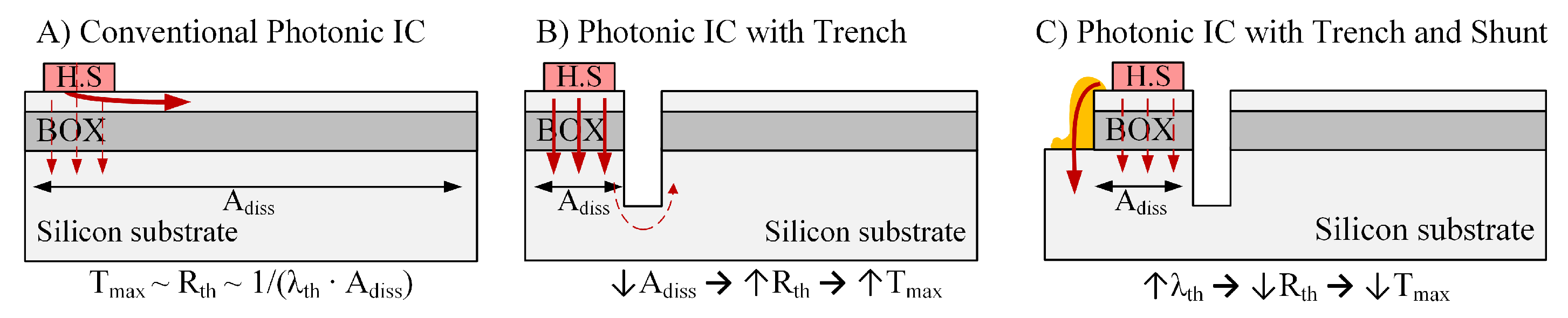
Figure 1A, heat flows first through the silicon-device layer of the photonic circuit before crossing the buried oxide layer, leading to large temperature gradients across the PIC.
Due to the large thermo-optic coefficient of silicon (
1/K [
25,
26]), silicon photonic devices and particularly phase-sensitive components are extremely sensitive to temperature. As the refractive index changes strongly with temperature, not only ambient temperature fluctuations, but also temperature offsets caused due to inefficient heat dissipation, as well as temperature gradients within the PIC, can cause the system to malfunction. Therefore, particularly in photonic systems with a large number of phase-sensitive components, such as future OPAs, thermal management becomes of utmost importance. In fact, investigations on the influence of undesired temperature changes on the functionality of OPAs have shown that not only the steering accuracy, but also the beam divergence and the side-lobe suppression are affected by temperature [
27]. Therefore, appropriate thermal management enabling efficient heat dissipation, as well as reduction of on-chip temperature gradients, is required [
28]. In addition, being consistent with the advantages of silicon photonics, thermal management solutions should allow for low power operation as well as for large-scale fabrication. One way to fulfill these requirements is to perform structural modifications in the PIC, so that temperature gradients are inherently reduced, the thermal resistance of the system is decreased, and therefore the demand for external cooling or heating is also diminished. Furthermore, to allow for large-scale fabrication, the structural modification should be compatible with the CMOS processes used for fabrication of the PIC. To this end, other groups have shown the use of so-called air trenches not only to improve the heating efficiency of thermo-optic modulators, but also to reduce the cross-talk between neighboring modulators [
29].
In this publication, two CMOS-compatible measures for thermal management of silicon photonic circuits are proposed. The efficiency of both concepts is determined experimentally by electrothermal characterization of in-house fabricated thermal demonstrators. As shown in
Figure 1B, the first approach proposes to use of trenches to separate the PIC in independent thermal regions. The region where the heat generating components are found, is called heat source region. The region where phase-sensitive components are located, is referred to as temperature sensitive region. The separation of the PIC in different regions allows to reduce thermal gradients in the temperature sensitive regions of the photonic chip. The second concept, shown in
Figure 1C, proposes the placement of so-called heat shunts, which are materials with high thermal conductivity between the heat source region and the silicon substrate. This allows bypassing of the thermally insulating silicon dioxide claddings, and therefore the improvement of the heat dissipation from integrated heat sources. To our knowledge, none of these concepts has been previously employed for thermal management of silicon photonic circuits. In
Section 2, both concepts are presented in detail and the concept of safe distances to quantify their efficiency is introduced. Then, in
Section 3 a brief overview on the fabrication, as well as the electrothermal characterization methods used, is presented. The results of the electrothermal characterization are presented in
Section 4. Finally, in
Section 5, the conclusions of the analysis are stated and a brief outlook on further investigations is provided.
2. Conceptual Description of Proposed Measures
Thermal management of silicon photonic systems has two major objectives: first, it must provide efficient heat dissipation, and also has to ensure for reduction of on-chip temperature gradients. The extreme temperature sensitivity of silicon photonic devices, combined with the high integration density achieved in photonic integrated circuits, makes thermal management crucial to guarantee for correct functionality of the system. Although, in most applications, temperature gradients play only a minor role, in photonic systems, consisting of a large number of phase-sensitive components such as in optical phased arrays, temperature gradients can largely influence the functionality of the system [
28]. Due to the large thermo-optic coefficient of silicon, its refractive index depends strongly on the temperature. In an OPA, where several hundreds or even thousands of phase-sensitive components are to be placed side-by-side, temperature gradients within the PIC would lead to a different refractive index and with it to a different optical phase in the individual channels of the array.
Due to their low thermal conductivity, silicon dioxide layers represent a major barrier for heat dissipation. Therefore, as shown in
Figure 1A, most of the heat dissipated by the active components spreads through the silicon device layer, where the photonic components are located, before crossing the SiO
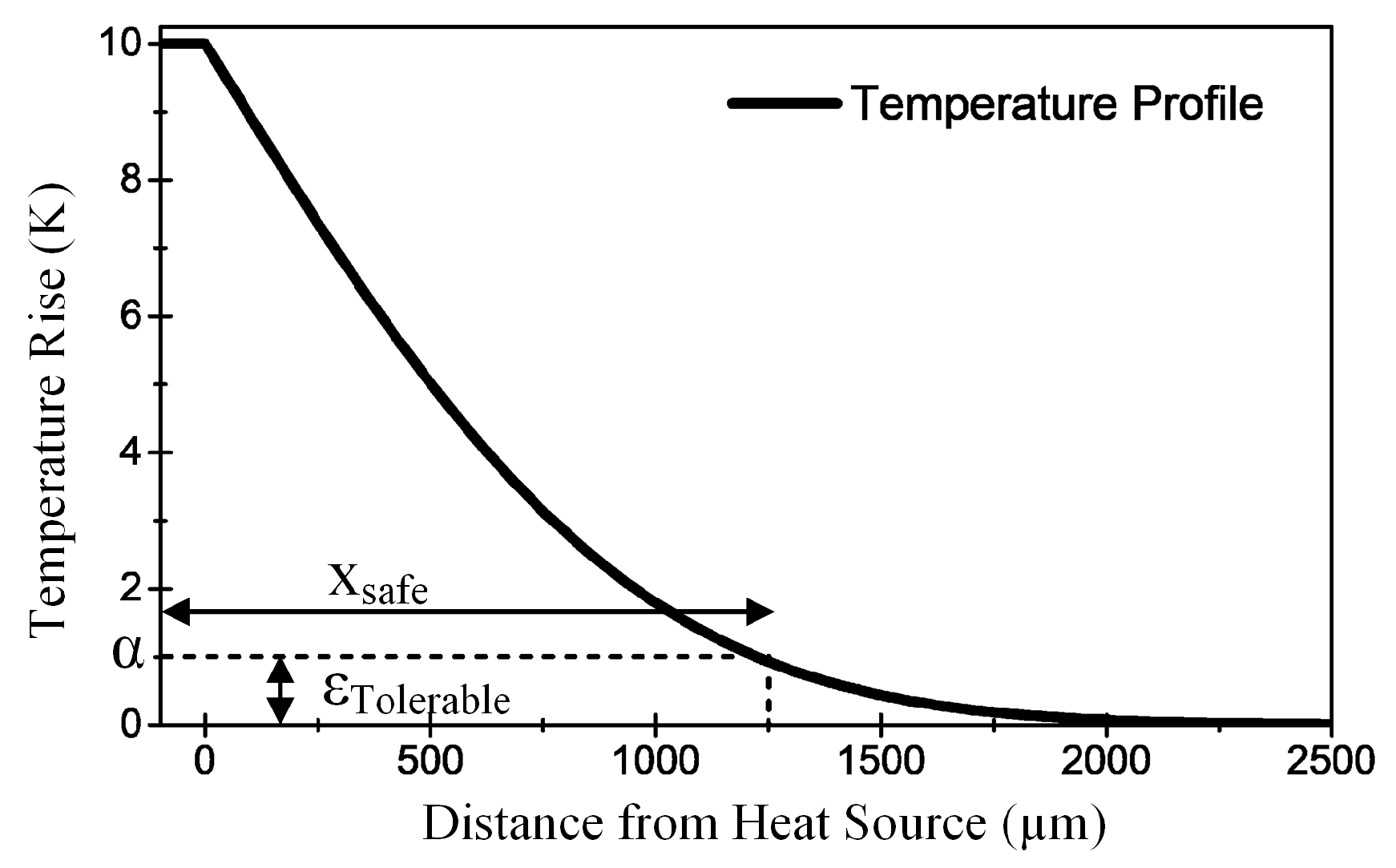
buried oxide layer. This results in temperature gradients such as the one shown in
Figure 2. To avoid the detrimental effects of temperature gradients on photonic devices, it might seem to be desirable from a thermal perspective to integrate electrically active components far away from temperature sensitive devices. However, increasing the distance between heat generating components and temperature sensitive components would reduce the integration density and therefore contradict one of the major advantages of silicon photonics. Therefore, thermal management of silicon photonic OPAs requires solutions to deal with the increased integration density, while improving the heat dissipation and reducing temperature gradients.
To assess the efficiency of the proposed measures in reducing temperature gradients, a new criterion referred to as safe-distance is introduced. The safe distance defines the distance from the heat source at which the temperature is smaller than a maximum tolerable temperature rise .
The temperature profile shown in
Figure 2 can be described by
where
is the heat sink temperature,
the maximum temperature of the body and
k a positive valued constant.
Mathematically, the safe distance
is defined as the distance at which the temperature difference between the coolest point of the system (i.e. T(x
)=T
) and the point at which the temperature rise equals a given value
(i.e.
). Rearranging Equation (
1) to
, the safe distance is found to be
where the maximum tolerable temperature rise
can be arbitrarily chosen according to the requirements of the particular application.
In optical phased arrays, where several phase-sensitive photonic components are used to form an array, reducing the safe distance is crucial, as this would allow to reduce the distance between heat generating components and the temperature sensitive components, increasing the integration density and finally reducing the costs of the system.
Being consistent with the advantages of silicon photonics requires the developed thermal management methods to be compatible with CMOS fabrication processes. In this way, these methods can be implemented in series production, during the fabrication of the PIC. In the following, a detailed description of both proposed CMOS-compatible thermal management measures is presented.
2.1. Trenches for Reduction of Temperature Gradients
The first concept to be discussed is the implementation of trenches to separate the PIC in two independent thermal regions, namely, the heat source region, where electric active components are integrated and the temperature sensitive region, where phase-sensitive photonic components are found. As shown in
Figure 1B, trenches are vertical cuts in the chip that allow for thermal separation of the heat source region from the temperature sensitive region. The missing physical contact between both regions forces heat to flow through the silicon substrate before reaching the temperature sensitive region. Due to the high thermal conductivity of silicon, heat spreads through the silicon substrate before crossing back the buried oxide layer, leading to small gradients in the temperature sensitive regions.
The efficiency of trenches in reducing temperature gradients depends on several parameters such as the trench depth and width. Although it seems evident that wider and deeper trenches would show a better performance than narrow and superficial trenches, increasing the trench width would increase the footprint of the PIC and increasing the depth of the trench would reduce the mechanical stability of the system threatening with reliability issues. Therefore, the ideal combination of trench width and depth must be found for each system.
One drawback of implementing trenches on the PIC is that due to the physical separation between the heat source region and the temperature sensitive region, the interconnection between both regions is limited. Although, due to the missing silicon device layer, the optical interconnection using lithographically defined waveguides is not possible, alternative methods such as photonic wire-bonding [
30,
31] or free-space coupling using 3D printed structures [
32] are still conceivable. Similarly, due to the missing physical contact between both regions, electrical interconnection is limited to the use of electrical wire-bonds. Although initially this could appear equivalent to using independent chips, integrating lasers and ASICs on the PIC substrate increases the integration density and reduces mechanical stability issues, particularly those associated with the precise alignment required between the laser and the in-coupling waveguide of the photonic IC.
An additional drawback of implementing trenches is the fact that compared to an un-trenched chip (
Figure 1A), the heat dissipation area (
) is reduced. As the maximum temperature (
) of the heat source is proportional to the thermal resistance (
), which is inversely proportional to the heat dissipation area [
33], reducing
would lead to higher
. Furthermore, since the thermal resistance is further increased with increasing trench depth, there is a trade-off between the reduction of the safe distance and the improvement of heat dissipation. In the following, the concept of heat shunts is presented as a possible way to reduce the increased thermal resistance.
2.2. Heat Shunts for Improvement of the Heat Dissipation
The second concept discussed here is the implementation of so-called heat shunts as thermal bridges between the heat source region and the silicon substrate. For this, as shown in
Figure 1C, heat shunts are fabricated using materials with high thermal conductivity and creating a physical connection between the heat source region and the highly thermally conductive silicon substrate. By fabricating shunts using materials with a higher thermal conductivity than that of silicon dioxide, they act as the preferred path for heat dissipation and shunt the heat flow through the thermally insulating silicon dioxide layers. Improving the heat dissipation would not only reduce the temperature of the integrated electronic devices, but a reduction of the maximum temperature would also contribute to reducing temperature gradients and therefore the safe distance.
Heat shunts can be fabricated using physical or chemical vapor deposition of materials with high thermal conductivity. However, it must be kept in mind that most of the highly thermally conductive CMOS compatible materials, also possess a high electrical conductivity, so that it must be ensured, that the shunt is not in contact with the heat source, otherwise it would cause a short-circuit in the system.
The magnitude of the improvement of the heat dissipation efficiency depends on the thermal conductivity of the shunt material as well as on the shunt geometry and thickness. The higher the thermal conductivity of the shunt material, the larger the improvement in heat dissipation. Similarly, the larger the area of the heat source region, which is covered by the heat shunt, the better the improvement will be.
To analyze the efficiency of both concepts, thermal demonstrators were fabricated and electrothermally characterized. From the results of the electrothermal characterization, the safe distances as well as the reduction in the thermal resistance of the system were calculated. In the next Section, a brief overview on the methods used for fabrication and for electrothermal characterization of the thermal demonstrators is presented.
3. Methods for Fabrication and Characterization of Thermal Demonstrators
The experimental results presented in this publication were obtained from the electrothermal characterization of in-house fabricated thermal demonstrators. All thermal demonstrators were fabricated on thermal oxide substrates with a silicon handle layer of 650 m thickness and 2.5 m thermal silicon oxide layer on top. Due to the similar layer thicknesses, the thermal behavior of thermal oxide substrates resembles well that of conventional SOI ( Silicon-on-Insulator) substrates.
The main building blocks of all thermal demonstrators are thin-film heaters, used to simulate the heat generating devices integrated in PICs, and thin-film thermometers used to measure the temperature at different points of the system. Thin film heaters make use of Joule heating to increase the temperature of the heater material. Joule heating, also known as resistive or Ohmic heating, refers to the heat up of a solid when an electrical current flows through it [
34]. Assuming that all the applied power
is dissipated as heat, the temperature rise of the heater is given by
, where
stands for the thermal resistance of the system,
for the electrical resistance of the heater and
I for the current flowing through the heater.
Thin-film thermometers are usually resistance based thermometers (RTD), so that the temperature of the system can be determined by measuring the change in electrical resistance. The relation between the electrical resistance and the temperature
T is given by
where
is the electrical resistance at the reference temperature
and
the temperature coefficient of the thermometer material. As shown in Equation (
3), the temperature coefficient
represents the slope of the
curve. Materials with linear temperature coefficients allow for accurate temperature measurement using few calibration points. Therefore, due to the linearity of its temperature coefficient in the temperature range of interest [
34], platinum (Pt) was chosen as the material for fabrication of the RTD thermometers. Furthermore, for simplicity of fabrication, i.e., to avoid deposition of different materials, heaters were also fabricated using platinum. In the following, a short description of the fabrication process as well as of the electrothermal characterization is presented.
3.1. Fabrication Methods
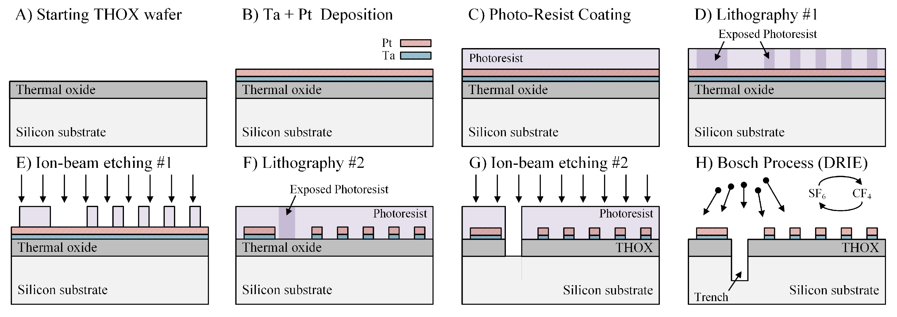
Thermal demonstrators were fabricated under clean-room conditions starting from six-inch thermal oxide substrates. The main processes required for fabrication of thermal demonstrators are (1) material deposition, (2) lithography, and (3) etching. The order in which the processes are used depends on the type of demonstrator being fabricated. In the following, the process used for the fabrication of trenched demonstrators is described in detail.
3.1.1. Fabrication of Trenched Demonstrators
The first step for the fabrication of the thermal demonstrators is PVD deposition of the metal layers to be used. Prior to the deposition of platinum (Pt), 15 nm of tantalum (Ta) is deposited on top of the oxide layer to improve adhesion of Pt to the SiO
. Due to its small thickness, making up for less than 5% of the total thickness, the Ta layer does not influence the linearity of the temperature coefficient of Pt. Afterwards, 315 nm of Pt is deposited on top of the Ta layer (
Figure 3B), and the wafer is spin-coated with photo-resist and prepared for the first lithography step (
Figure 3C). In this step, a laser writer is used to expose the photo-resist and define the geometry and the arrangement of the heaters and thermometers (
Figure 3D). After the first lithography step, the resist is developed removing unexposed photo-resist, so that only the heater and thermometers structures are covered by the photo-resist (
Figure 3E). The remaining metal areas are then removed by ion-beam etching (IBE) and the photo-resist is removed by plasma cleaning. Then, a second lithography step is used to define the position where the trenches will be found (
Figure 3F), and the silicon dioxide layer is removed by ion-beam etching (
Figure 3G). Once the SiO
has been removed, the trenches in the silicon substrate are created using the so-called Bosch Process (The Bosch Process also known as deep reactive-ion etching (DRIE) is an anisotropic etch process with which high aspect ratio structures can be obtained. To achieve the high aspect ratio the etching gas (SF
) and the protecting gas (C
F
) are switched in a repetitive manner.) (
Figure 3G).
For the fabrication of heat shunts, additional steps are required. In the following, the process used for fabrication of demonstrators with heat shunts is briefly described.
3.1.2. Fabrication of Heat Shunts
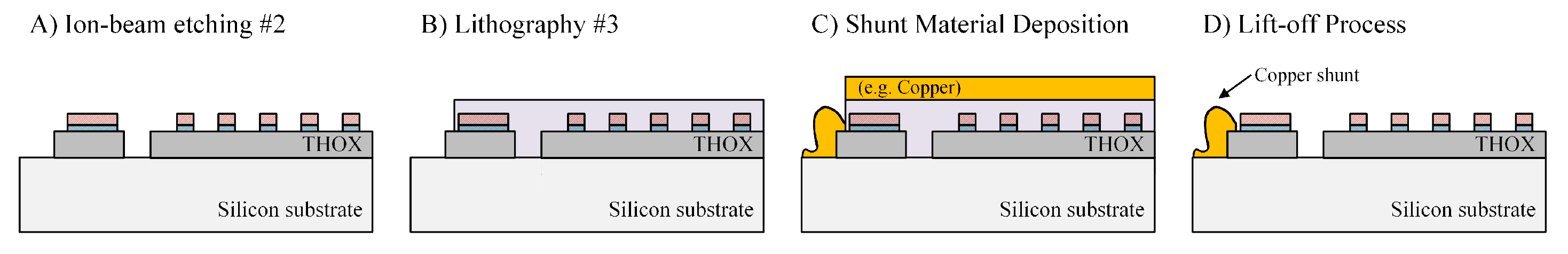
The starting point for the fabrication of thermal demonstrators with heat shunts is the second IBE step (
Figure 3G) from the trenched demonstrators. The main difference relies in the fact that at this point, rather than starting straight the DRIE etch process, the resist is removed and a third lithographic step is used to define the position where the heat shunts will be found (
Figure 4B). A further difference is that during the lithography step a so-called lift-off photo-resist is used and is removed from the position where the shunts will be located. Once the position of the shunts has been defined, the shunt material is deposited (
Figure 4B). For this investigation, due to its high thermal conductivity, copper was chosen as shunt material
. Note that to guarantee a physical connection between the heat source and the silicon substrate, the thickness of the shunt material must be greater or equal than the thickness of the thermal oxide layer. In this case, a thickness of 2.5
m is used. After the material has been deposited, the lift-off process is realized; removing the photo-resist and leaving the shunt material only in the previously defined regions (
Figure 4D).
From this point, if trenches are also desired, the DRIE etch process can be started. Once the clean-room fabrication is finished, the wafer is diced into individual dies, which are used for electrothermal characterization.
Precise description of the individual fabrication processes are out of the scope of this paper and therefore not presented here. For comprehensive information on these processes the reader is referred to specialized literature [
35,
36].
3.2. Electrothermal Characterization Methods
After the thermal demonstrators are successfully fabricated and the wafers are diced, the individual chips are electrothermally characterized. In
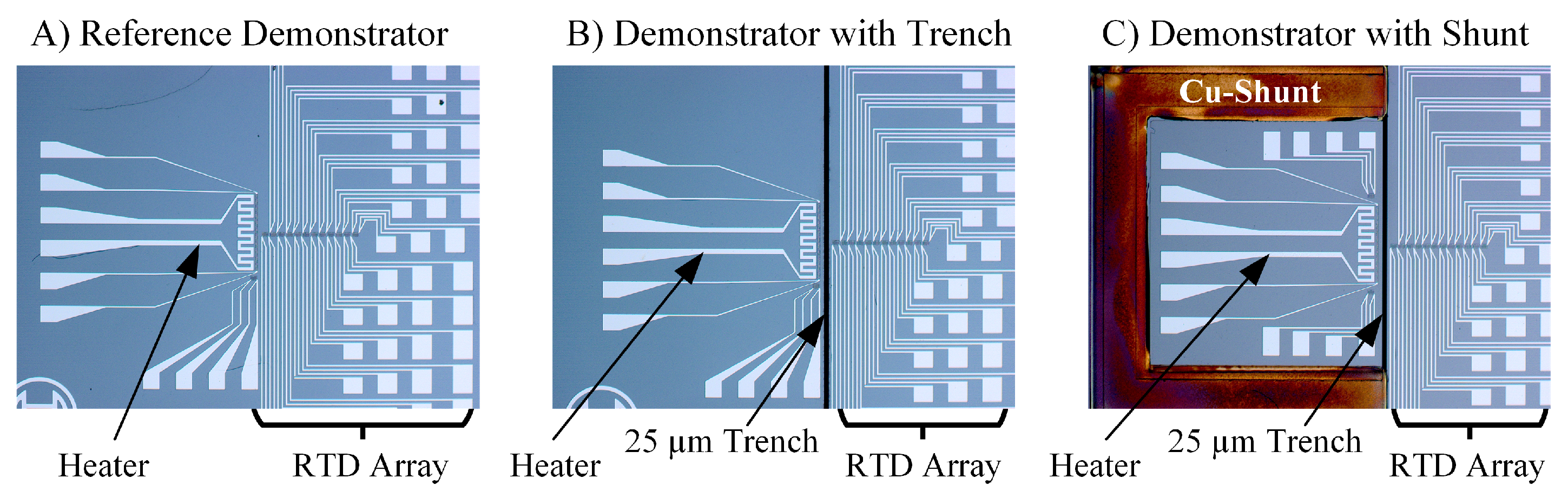
Figure 5, microscope images of the three types of thermal demonstrators are shown. The first one (
Figure 5A), which is called reference demonstrator, is a chip without trenches or shunts and is used to obtain a reference of the thermal behavior of the system. This reference is necessary to determine the reduction of the safe distance when trenches are included or the improvement of heat dissipation when shunts are used.
The left side of the image, where the heater is located, corresponds to the so-called heat source region and the right side of the image to the temperature sensitive region. To determine the temperature profile in this region, an array of RTD thermometers is used. An additional thermometer is placed in the heat source region, 10
m away from the heater, to determine its temperature at different applied powers.
Figure 5B shows a trenched demonstrator with a trench width of 25
m.
Figure 5C shows a demonstrator with a trench and a copper shunt.
Regardless of the type of demonstrator, the first step in the electrothermal characterization is the calibration of the fabricated structures. As the measurement principle of the fabricated thermometers relies on the measurement of the electrical resistance to eliminate the influence of the connection lines on the measurement, a four-point measurement is performed. Using this approach, the resistance thermometers are calibrated by applying an electrical current and measuring the voltage drop across the thermometer structure at different temperatures. To avoid self-heating effects of the thermometers during the measurement, the measuring current is chosen as 1 mA. Furthermore, for the thermometer calibration, the stage where the chips are placed is heated to the desired temperature. The stage temperature can be measured with an accuracy of 0.1 K.
From the voltage drop measured at the different calibration temperatures, the temperature dependence of the electrical resistance is calculated. To reduce possible errors, the voltage measurement at each calibration temperature is repeated hundred times and the average voltage is used for the calculation of the resistance. Additionally, to improve the accuracy of the temperature measurement, despite the linearity of the temperature coefficient of platinum, a three-point calibration is used instead of a simple two-point calibration.
Once the thermometers are calibrated, an electrical heating power is applied to the heater and the temperature profile across the chip is determined by measuring the temperature of the individual thermometers in the array. The temperature is determined from the electrical resistance of the thermometers, using the temperature dependence of the electrical resistance found during the calibration. The electrical resistance itself is calculated from the applied measuring current and the measured voltage drop. The largest measurement error of the RTD thermometers is calculated, and it is assumed to be equal for all thermometers. Although most thermometers are capable of more accurate measurements, for the evaluation of the measured data the error was assumed to be 1.1 K.
In the next section, the results of the electrothermal characterization of the different demonstrators, as well as the influence of the proposed measures on the reduction of the safe distance, are presented.
4. Experimental Evaluation of Proposed Measures
Using the calibrated thermometers, the thermal behavior of the different demonstrators can be analyzed. To compare the behavior of the different demonstrators, the maximum chip temperature, the lowest temperature of the chip, and the temperature profile along the thermometer array are measured. As mentioned above, the thermometer used for determination of the heater temperature is placed 10 m away from the heater. The thermometers in the RTD array are placed at a distance of 50 m from each other and cover a region of ~1000 m away from the heater, as this was found to be the region where the temperature gradients are the largest. The lowest temperature of the chip is measured using thermometers placed at large distances (i.e., m) from the heater.
The temperature measurements are plotted over the distance from the heater and the exponential function in Equation (
1) is fitted to the measured data points. From the fitted function, the safe distances are calculated according to Equation (
2). For the calculation of the safe distances, the maximum tolerable temperature rise
was chosen to be 1 K, as this is an acceptable value for the temperature difference across the OPA. Note that, despite the temperature profile as described by Equation (
1) does not takes into account the missing material in the trenched region, to maintain the comparability between the experimental results, the exponential function is always fit over the complete chip dimensions (i.e., over both regions). Additionally, fitting the exponential curve over both regions, allows for direct estimation of the heat source temperature, which is a direct measure for the thermal resistance of the system.
In the following, the experimental results obtained from the electrothermal characterization of the different thermal demonstrators are presented. First, the temperature profiles as well as the heater temperature obtained from the measurement of the reference demonstrators (the demonstrators without trenches or shunts) at three different heating powers are presented. This is used to observe the influence of the heating power on the heater temperature, as well as on the safe distances within the demonstrator. Then, the results obtained from the trench demonstrators are shown and the influence of the trench depth and width on the reduction of the safe distances is presented. Finally, the thermal demonstrators with heat shunts are presented. In this case, the influence of heat shunts on the thermal resistance of the system is investigated by measuring the temperature rise for different heating powers. Then, the influence of the implementation of heat shunts in trenched demonstrators on the reduction of the safe distance is analyzed by comparing the measured temperature profile for trenched demonstrators with and without shunt.
4.1. Reference Demonstrators—Influence of the Heating Power
The first sample to be characterized is the so-called reference demonstrator. As shown in
Figure 5A, this sample contains only the heater and the array of thermometers and is used as reference to evaluate the modifications of the thermal behavior of the chips, once one of the proposed thermal management measures is applied.
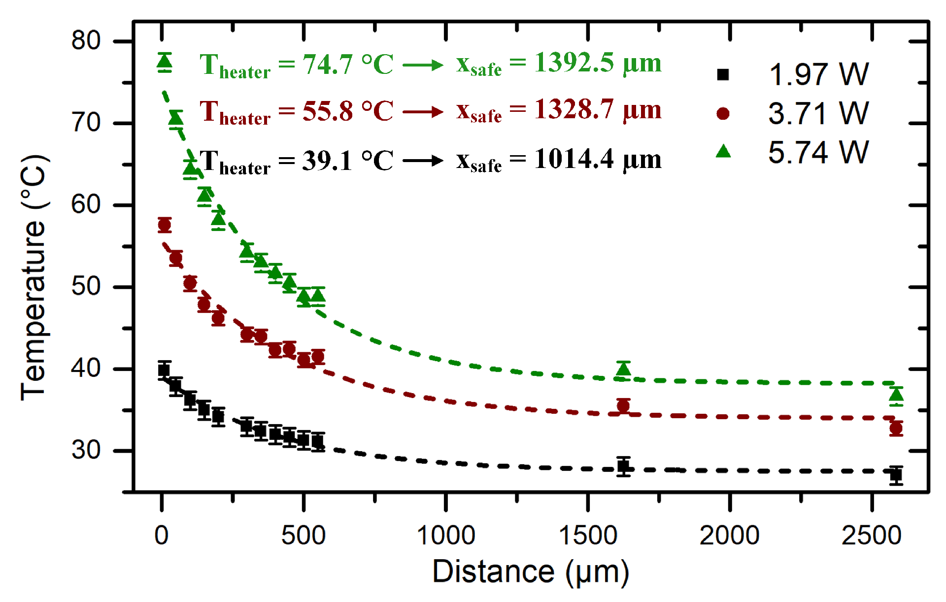
Furthermore, as traditional thermal management approaches suggest a reduction of the dissipated power, the thermal behavior of the reference sample for three different heating powers is investigated. The temperature profiles measured in the reference sample are shown in
Figure 6.
The dashed lines correspond to the fit of the measured data using Equation (
1). Using these fits, the safe distances for the different heating powers are calculated. In
Figure 6, the maximum measured temperatures and the calculated safe distance for the different heating powers are presented. Although a reduction of the heating power decreases the maximum temperature
, the reduction in the safe distances is considerably smaller than the power reduction. For instance, reducing the power by ~50% (from 3.71 W to 1.97 W) reduces the temperature increase by ~30% (from 55.8
C to 39.1
C) and the safe distances by ~25% (from 1328.7
m to 1014.4
m). In addition to having only a small influence on the safe distance, reducing the power dissipation (the heating power) is not always possible. Therefore, alternative approaches for thermal management with a larger influence on the safe distances must be found. In the following, the results obtained from the electrothermal characterization of trenched demonstrators are presented and the influence of trenches on the safe distance is determined.
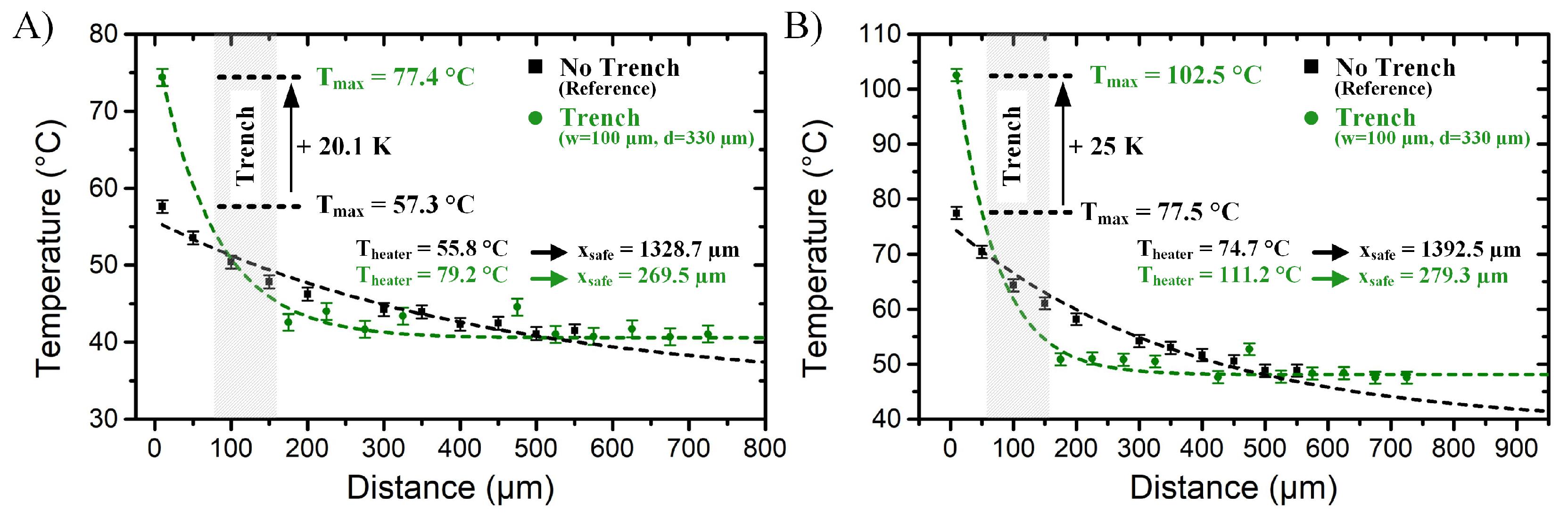
4.2. On Silicon Trenches for Reduction of Temperature Gradients
As described in
Section 2, the main idea behind the use of trenches is to separate the PIC in two thermally independent regions: the region were heat generating components, such as ASICs and lasers, are placed, is called the heat source region, and the temperature sensitive region, where temperature sensitive photonic components are found. Furthermore, the major drawback from this approach is the fact that due to the reduced area for heat dissipation, the thermal resistance of the system rises, increasing the temperature rise of the heat generating components. Therefore, the electrothermal characterization of trenched demonstrators must provide information not only in the reduction of the safe distance, but also on the increase of the maximum temperature. Although the trenched demonstrators are also characterized using three different heating powers, for clarity only the results for the highest heating power (
= 5.74 W) are presented.
Figure 7 shows the comparison of the temperature profile of a thermal demonstrator without trench (black) and that of a demonstrator with 330
m deep and 100
m wide trench (green).
The gray rectangle in
Figure 7 represents the position where the trench is found. The heat source region is the region left from the rectangle and the region right from the rectangle is the so-called temperature sensitive region. As expected, the maximum temperature increased from 77.5
C to 102.5
C (~25%). However, despite the temperature increases in the heat source region, the maximum measured temperature in the temperature sensitive region (right from the trench) was reduced from 58.2
C to 50.9
C (~15%) and the safe distance was also reduced from 1392.5
m to 279.3
m (~80%).
To find the relation between the trench depth and width on the safe distance, as well as on the heater temperature, thermal demonstrators with three different widths and three different depths were characterized. Narrow trenches with widths of 25 m, 50 m, and 100 m are chosen to avoid unnecessary increase of the footprint of the PIC. Similarly, the trench depths were limited to about half of the wafer thickness to avoid strong reductions in the mechanical stability of the chips.
The calculated safe distances and the heater temperatures (
) obtained from the fit for the different trench widths and depths at constant heating power (
= 5.74 W) are presented in
Table 1.
Although in demonstrators with superficial trenches the safe distances decrease with increasing trench width, for demonstrators with deep trenches the safe distances increase with increasing trench width. Furthermore, in all cases the trench depth has the largest influence on the reduction of the safe distances. It can be also observed that heater temperature increases with increasing trench depth and with increasing trench width. Regardless of the demonstrator being characterized, the influence of the trench depth on the heater temperature is larger than that of the trench width.
To solve the problem of the increased heater temperature, the concept of heat shunts is analyzed. Heat shunts provide a high thermal conductivity path between the heat source region and the silicon substrate, allowing thermally bypassing the insulating SiO claddings; this reduces the thermal resistance of the system and therefore the temperature of the heater.
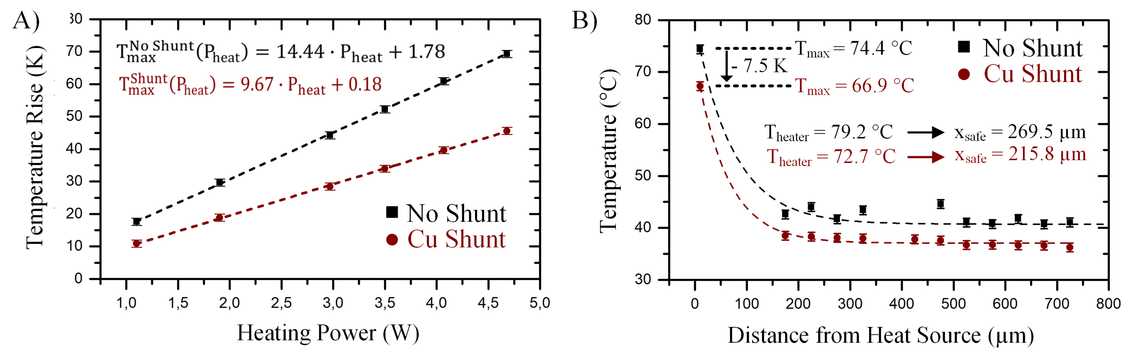
4.3. Heat Shunts as Thermal Bridges for Improvement of Heat Dissipation
Implementing heat shunts intends to improve the heat dissipation by creating a high thermal conductivity path between the heat source region and the silicon substrate of the PIC. Thermally bypassing the silicon dioxide cladding layers would reduce the thermal resistance of the system and with it the heat source temperature. The reduction of the thermal resistance is found by plotting the maximum measured temperature for different heating powers. Then, as shown in
Figure 8A, comparing the slope of a linear fit going through the measured data, the reduction of the thermal resistance is determined.
It can be seen that including 2.5 m copper heat shunts around the heat source, reduces the thermal resistance by ~30% (from 14.44 K/W to 9.57 K/W).
The influence of using these copper heat shunts in a trenched demonstrator is also investigated. As shown in
Figure 8B, the temperature profile along the RTD array of a trenched demonstrator without heat shunts is compared to that of a demonstrator with shunts. As previously mentioned, the measured data are fitted using the exponential function from Equation (
1) and the safe distances are calculated according to Equation (
2). The resulting heater temperature obtained from the exponential fits as well as the calculated safe distances are also presented in
Figure 8B. Using heat shunts in a trenched demonstrator not only reduces the heater temperature by ~10% (from 79.2
C to 72.7
C), but also reduces the safe distances by ~20% (from 269.5
m to 215.8
m).
5. Conclusions
In this publication, two CMOS-compatible concepts for thermal management of silicon photonic circuits were presented and their efficiency was experimentally validated by in-house fabrication and electrothermal characterization of thermal demonstrators. In addition, calculations regarding their efficiency were made, taking geometrical parameters into account. In the first concept, trenches into the silicon substrate are used to separate the PIC in independent thermal regions. The second concept proposes to use heat shunts to bypass the thermal insulating silicon dioxide claddings and therefore to improve the heat dissipation of integrated heat sources.
From the results presented above, we conclude that trenches are extremely efficient for reducing on-chip temperature gradients. In the fabricated demonstrators, using trenches allowed reducing the safe distances by up to 80%, from 1400 m for a non-trenched (conventional) chip to ~280 m for a chip with a 330 m deep trench. The major drawback of using trenches is the reduced heat dissipation area, which leads to an increased thermal resistance of the system. In the fabricated demonstrators, the increased thermal resistance caused a ~30% increase of the heat source temperature (from 74.7 C for the non-trenched chip to almost 111.2C for the chip with the 330 m deep trench). Still, the benefits of using trenches outweighs this detrimental effect.
However, to neutralize this drawback, the use of heat shunts in addition to trenches is proposed. Heat shunts provide a preferred path for heat dissipation, reducing the heat source temperature. Placing 2.5 m-thick copper shunts around the thin film heaters reduces the thermal resistance of the system from 14.44 K/W to 9.67 K/W. In the case where heat shunts are combined with a trench of 330 m depth and 100 m width, the temperature rise is reduced by ~10%, from 74.4 C to 66.9 C, and the safe distance is reduced from 269.46 m to 215.84 m (~20%).
Although additional methods to improve the heat dissipation are still required, in its present form, the proposed measures allow for a considerable increase of the integration density, potentially allowing not only the reduction of the system dimensions, but also of its total costs, while maintaining the system performance. Furthermore, although both concepts show promising results, additional investigations are still required. First, to fully understand the influence of trenches in the reduction of safe distances, additional depths and widths must be investigated. Then, the influence of the shunt thickness, geometry, and material on the heat dissipation must also be investigated. It is expected that by using materials with higher thermal conductivity, or using thicker shunts, the improvement in the heat dissipation efficiency would be even greater than this reported here. Similarly, we propose the use of thermally conductive but electrically insulating materials for the shunts. In this way, it would be possible to create a direct contact between the heat source to the silicon substrate, allowing for even larger improvements in the heat dissipation efficiency. Additionally, as in silicon photonic circuits the thickness of the cladding layers is easily changed, similar investigations with substrates having different thermal oxide thicknesses should be performed. Also, reducing the width of the trench to single micrometers, while maintaining a high trench aspect ratio, could enable the use of trenches to confine the heat from thermo-optic modulators. This would not only increase the integration density, by allowing to reduce the distance between modulators, but by increasing the thermal resistance of the system, it would also reduce the required electrical power to achieve a given temperature, increasing the power efficiency of the system. Although it is clear that there is still plenty of room for extensive investigations, such investigations are out of the scope of this publication and therefore are not presented here.
In addition, although, in its current implementation, the trenches limit the options for optical and electrical interconnection, additional investigations allowing to maintain the strictly required material for interconnection would enable the use of trenches with fully integrated components, potentially allowing the flip-chip integration of ASICs on top of photonic circuits.
Finally, it must be noted that although the proposed methods are proposed for silicon photonic OPAs, they can be used in any other silicon photonic application, in which phase-sensitive elements such as Mach–Zehnder interferometers or ring resonators are used, and in which efficient thermal management is required. The proposed methods could also be used in other non-photonic applications, in which the temperature profiles need to be tailored.


