1. Introduction
Photoconductive antennas are an established technology for THz detection in commercial continuous wave (CW) spectrometers [
1]. Their use in applications other than spectroscopy, such as communication [
2,
3] and non-destructive testing [
4,
5,
6], has been fostered by the introduction of photoconductive antennas (PCAs) compatible with 1550 nm telecom laser technology [
7,
8]. These laser systems benefit from the large availability of inexpensive, powerful optical components of the telecom industry.
A full characterization of the PCAs performance as THz detectors is still difficult. In most cases, only the system dynamic range is specified [
9,
10], which is a relative figure of merit, composed of the source performance and receiver performance. International System of Units (SI) traceable noise floors and power levels are seldomly specified. To the knowledge of the authors, the only SI traceable characterization has been performed on pulsed PCAs in [
11,
12].
In this work, we experimentally characterize the noise-equivalent power (NEP) and the responsivity of two PCA homodyne CW THz detectors, and develop a theoretical model for them. The experimental characterization is performed by measuring the detected current and the noise floor of the PCAs when a THz PIN diode is used as an emitter; then, the PCAs are replaced by a pyroelectric detector, and the emitted power is measured under exactly the same conditions. Since the THz power is measured with a pyroelectric detector calibrated by the National Metrology Institute of Germany (PTB) [
13], the figures of merit obtained under these conditions are directly traceable to SI units. The characterization incorporates the DC properties of the detectors as well as a comparison with the DC properties of a third detector with similar properties. The first two characterized THz detectors are ErAs:InGaAs PCAs with a 10
m × 10
m active area covered by a finger electrode structure which is coupled to a self-complementary logarithmic-periodic antenna. The photoconductive material consists of a periodic structure of alternating layers of 10 nm of InGaAs and Be-delta-doped 0.8 monolayers of ErAs repeated 90 times. The third detector, used only for the DC comparison, is identical to the first two but instead of being Be-doped, it was C-doped, as described in [
14]. All three detectors were designed and processed at Technische Universität Darmstadt with material grown at the University of California, Santa Barbara solely for research purposes.
The experimental characterization is performed for the frequency range between 100 GHz and 1 THz. The obtained results are compared with theoretical predictions. The theoretical model is elaborated in
Section 2. The setup for the experimental characterization and the conditions in which it was performed are described in
Section 3. The comparison between the experimental and the theoretical results is presented in
Section 4. Brief concluding remarks are given in
Section 5.
2. Theoretical Model for the NEP and Responsivity of PCAs
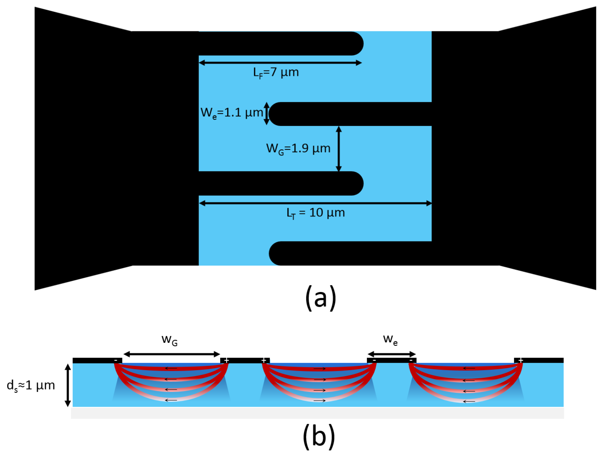
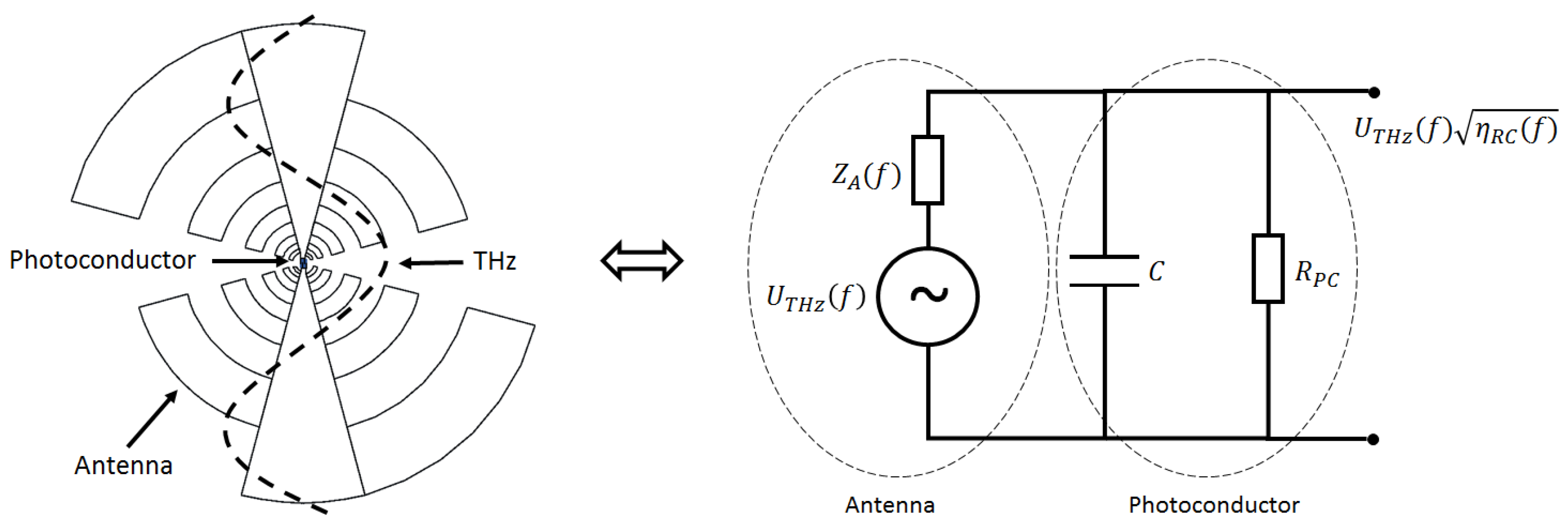
A PCA coherent THz detector with a finger-electrode structure as shown in
Figure 1a generates a rectified current
where
f is the THz frequency (frequency difference between the lasers driving the PCA),
t time,
j the current density,
the spatial coordinate in the cross section area, and
the meander-like cross section area between the finger electrodes on the absorbing photoconductive layer with thickness
and meander length
.
The total length can be approximated to
with
N the total number of fingers,
the finger length,
the finger width, and
the photoconductive gap size, as shown in
Figure 1a.
The current density generated by holes or electrons has been derived in [
15], Equation (
9), to
with
,
the laser power at depth z,
the absorption coefficient,
the frequency of the laser driving the PCA,
the average carrier velocity at depth
z,
the carrier lifetime (assumed to be the same for holes and electrons) and
the lifetime roll-off for the current. The absolute-square of
is the well known lifetime roll-off for the THz power. The term
can be understood as the photoconductive gain which is, as we will show, linearly dependent on the received THz field.
The average carrier velocity
originates from the THz bias
produced in the antenna when THz power falls on it, with
n being the total amount of generated carriers and
the amount of carriers at depth
z. Its value, weighted by the amount of carriers, is given by
, where
is the respective carrier mobility and
is the (effective) THz field in the gap which is proportional to the THz bias delivered by the antenna that drops along the gap width,
. The efficiency
accounts for the inhomogeneity of the field between the electrodes (as shown by the field lines in
Figure 1b), and for the variation of carrier density as a function of penetration depth with
z as a weighting factor. The term
is the power RC roll-off, where
is the antenna impedance, and
C is the device capacitance, as shown in the equivalent circuit of the PCA in
Figure 2. The effect of photoconductor resistance
is usually negligible for the RC roll-off under CW operation conditions, where typically
and
. For the PCAs analyzed here and the frequency range of interest, electromagnetic (EM) simulations show that
achieves a maximum of 125.75
and that
C equals 3.7 fF, resulting in a maximum of 442
for
. The measured value of
is between 12.8 k
and 16.66 k
. Hence,
is at least 30 times higher than
and at least 100 times higher than
, thus, its effect can be considered negligible.
Since the effective mass of (heavy) holes
is about nine times larger than that of electrons in In
Ga
As, the mobility of holes,
, is estimated to be about nine times smaller than that of electrons (assuming similar momentum scattering times
for both electrons and holes). Therefore, holes play only a minor role in the current generation mechanism, and only electrons are taken into account. With that consideration, the substitution of all terms into Equation (
1) yields
The phase difference accounts for the optical path length difference between source and receiver; here, we are only interested in peak values, hence, we set . is the ideal photocurrent amplitude for the total incident laser power . The optical efficiency takes into account that not all the incident laser power is absorbed within the photoconductor of thickness .
The THz bias is related to the incoming THz power
by
with
the real part of
and
the coupling efficiency of the THz beam to the antenna, which takes into account the mismatch of the THz spot size to the effective antenna cross section and the silicon lens reflections. The value of
in the equivalent circuit is the peak value of voltage source that would re-radiate all the incoming
if the output terminals of the antenna were left open (i.e., the Thevenin equivalent open-circuit voltage source) as explained in [
16]. A generalized formulation for broadband excitation would require substituting the powers by spectral densities. For the case of broadband pulsed excitation, the derivation for emitted power can be found in ref. [
17].
The detected current as a function of the THz power can then be written as
where
denotes the time average, i.e., the DC component.
The unknowns
and
can be determined by a measurement of the DC resistance, since Equation (
4) is also valid at DC if one substitutes the THz bias
by the DC bias
. This results in
. Equation (
4) then becomes
with
being the DC resistance of the PCA under illumination. Ultimately, we can define the THz power responsivity
as
with
Except for
, which is alignment-dependent, all the parameters in Equation (
9) can be obtained from EM simulations
or from previous measurements
, as it will be shown in
Section 4. This, however, assumes that the DC and THz material parameters of the photoconductor are identical, which may not generally be the case. As an example, the DC mobility as obtained from Hall measurements is well suited to determine the DC resistance of the sample. However, under THz conditions, the carriers are only inadequately described by a constant mobility which describes the constant average velocity,
, for a carrier in an electric field. On the one hand, photocarriers are generated at rest and then accelerated to
, generally leading to smaller average velocities as predicted by the DC mobility; further, the acceleration period may have influence on the frequency response under pulsed operation. For CW, however, non-harmonic and higher harmonic contributions average out, allowing to describe the carrier velocity by an average value. On the other hand, intrinsic samples with few scattering centers can even show a velocity overshoot [
18]; but it is generally accepted that a velocity overshoot is not expected for photoconductors due to scattering with trap states and the short carrier lifetime. We therefore expect that the mean velocity of photogenerated electrons on the sub-ps time scale, relevant for THz rectification, is smaller than the average DC velocity
relevant for DC measurements. An exact determination of the carrier motion on a THz time scale requires further pump-probe measurements on the sub-ps time scale that go beyond the scope of this paper. Hence,
is the only fitting parameter in our model of the responsivity. In general,
might be a function of frequency, but for the frequency range of interest, between 100 GHz and 1 THz,
is indeed fairly frequency-independent. The reason is that the effective receiving area in the PCA detector given by the broadband logarithmic-periodic antenna and the diffraction-limited spot size of the incident THz power scale with frequency in the same manner (area
). Further the emitter and the detector use self-complementary antennas. Even if there is a mismatch between the effective receiving area and the THz spot size, the mismatch will remain the same through the whole frequency range of interest due the frequency-independent properties of self-complementary antennas. Only at frequencies below 150 GHz, the THz spot is diffraction-limited by the finite aperture of the silicon lens attached to the detectors. This results in further Airy focusing and in a slight shift in the focal point of the THz spot, reducing the coupling efficiency. Other than that, the reflections at the surface of the silicon lens (due to the mismatch between the refractive index of silicon and air) remain constant for the whole frequency range.
Considering the differences between AC and DC performance, a more appropriate formulation of Equation (
9) for CW operation is
While the THz mobility is unkonwn, the DC mobility can be obtained from Hall measurements. Given that we cannot discriminate experimentally between inefficient coupling and differences in the mobility, we define an effective THz efficiency .
Finally, we derive an equation for the NEP, defined as the amount of power required to have a signal-to-noise ratio of one. The ideal NEP can then be expressed as
where
is the THz NEP (with units W/Hz) and
is the thermally limited noise, being the lower limit for the noise current density if further noise sources, such as undesired incoupling of stray fields or amplifier noise are absent.
Substituting Equation (
9) and using
into Equation (
11) yields
We remark that the derivation so far assumed that the photoconductor resistance,
, is much larger than the radiation resistance of the antenna,
, i.e., it is mismatched. This is the usual case for CW operation. For pulsed operation, however,
may become comparable to or even smaller than
, at least for short times. In this case, the
in Equation (
12) needs to be modified by reevaluation of the equivalent circuit in
Figure 2 [
12]. As an example, in the extreme case of
, the THz bias generated by the antenna drops almost completely at
(i.e., it is re-radiated) and only negligible bias drops at the photoconductor. The device stops working efficiently.
3. Experimental Setup
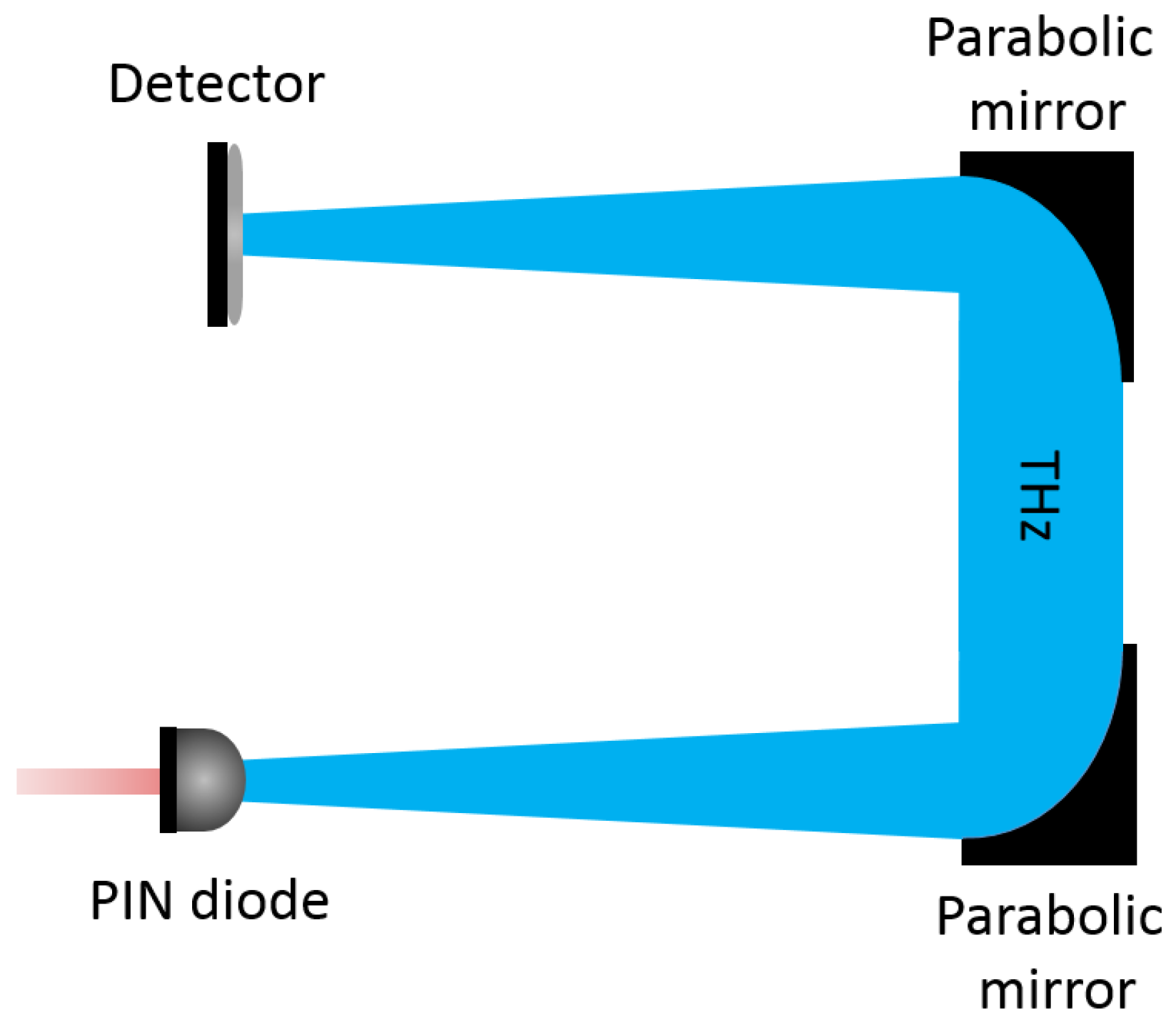
Two THz setups, both using the TeraBeam 1550 system from Toptica Photonics, were used for the experimental determination of the NEP and responsivity of the two ErAs:InGaAs PCAs, henceforth PCA A and B (
Figure 3).
First, the power of a PIN diode, used as the THz emitter to characterize both PCAs, was measured using a pyroelectric detector calibrated by the PTB. To do so, a lock-in amplifier was connected to the detector in order to read out the root mean square (RMS) value of the detected voltage. A second calibration was required in order to transform the RMS value (measured by the lock-in amplifier) into a peak-to-peak value (measured by an oscilloscope at the PTB). The PTB calibration of the detector was performed with a maximum error of 5%, and it allowed to measure a minimum power of 1 W. The calibration of the lock-in amplifier RMS value with respect to the oscilloscope peak-to-peak value featured an error of 2% (after a total of 10 measurements).
The setup used for the power measurements employed two parabolic mirrors (with a diameter of 5.08 cm, and focal length of 7.62 cm) to collimate and focus the THz radiation from the THz PIN diode. The pyroelectric detector was placed at 5.5 cm from the focusing mirror, the same distance at which the PCA detectors were placed. The THz PIN diode was biased with a 15.5 Hz square signal to produce a slow THz ON/OFF modulation as required by the pyroelectric detector due to its slow response time. In order to completely shut down the THz emission, a forward bias of 0.5 V was always applied during the OFF part of the modulation cycle. For the different THz powers required to determine , different reverse biases between −0.2 V and −1.1 V were applied during the ON part of the modulation cycle. For the experimental characterization of the NEP and the responsivity, the reverse bias was kept constant at −1.1 V during the ON part. The optical power arriving at the PIN diode was 26 mW ± 0.7 mW during the characterization of PCA A, and 22 mW ± 0.3 mW during the characterization of the PCA B.
Second, the pyroelectric detector was replaced by the PCAs. The modulation frequency was increased to 1983 Hz in order to reduce noise. We verified that the current amplitude detected by the PCA with a modulation frequency of 15.5 Hz frequency was identical to that detected with 1983 Hz, confirming that the THz power is not affected by modulation speed of the PIN diode. The PCAs were connected to a transimpedance amplifier (TIA) with a gain of 3.3 × 10 V/A, and then to a lock-in amplifier. The laser power from the TeraBeam 1550 arriving at PCA A during its characterization was 25.3 mW ± 0.6 mW, while the laser power arriving at PCA B during its characterization was 24.7 mW ± 0.9 mW. This results in an uncertainty of 3.6% in the measured laser power arriving at the PCAs, and hence, in the NEP.
The laser power at the THz PIN diode and the PCA detectors was defined by the output power of the DFB lasers of the TeraBeam 1550. The laser power arriving at all the devices was measured with an optical power meter after the THz measurements were performed. The differences in the measured laser power between the characterization of PCA A and PCA B were caused by the use of different fibers. Variations in the measured laser power arriving at the PIN diode result in differences of the THz power. These differences are calibrated by THz power measurement with the PTB-calibrated detector and therefore do not affect the NEP measurement. Variations in the measured laser power arriving at the detectors, however, may alter the NEP and the responsivity. As discussed in Ref. [
14], the NEP saturates at high laser powers,
, and then variations of
have no influence on the NEP. For low laser powers, the NEP is proportional to
according to Equation (
12), resulting in a (worst case) NEP uncertainty of 3.6%. The geometric mean of all known uncertainties in the NEP then accounts to 6.5%. The responsivity, according to Equation (
9) is proportional to
, thus, its uncertainty due to the errors in the laser power measurements is 7.2%. The geometric mean of all known uncertainties in the responsivity accounts then to 9%.
Remaining uncertainties are alignment errors. The PTB-calibrated power detector features an area much larger than the THz spot size, easily capturing all incoming THz power, while the PCA, with an effective receiving area in the range of the THz spot size, requires excellent alignment to achieve the same. The remaining uncertainty is therefore the alignment error of the PCA to the THz spot. As there are no means to access this quantity accurately, the alignment uncertainty is swallowed in the only fitting parameter . All values presented in the following are therefore extrinsic. The intrinsic detector NEP may be much lower and the responsivity much higher than the presented values, leaving room for future improvements of the detector design.
4. Results
In order to compare experimental results to the theoretical model, i.e., the DC resistance (Equation (
7)), the responsivity (Equation (
9)) and the NEP (Equation (
12)), several material parameters and electrical parameters are required. The carrier mobility and carrier concentration for PCA A, PCA B and the receiver shown in [
14], henceforth termed PCA C, were measured by high resistance Hall measurements (Lakeshore 8400). The two wafers show nominally the same layer structure, except that the PCA A and PCA B are Be-doped while PCA C is C-doped. The mobility of the wafer of PCA A and B has been found to 186 cm
/Vs while that of PCA C was 775 cm
/Vs. The carrier concentration has been determined to
cm
and
cm
. We note that these values are only about 14 times (54 times) higher than the intrinsic carrier density,
, of InGaAs. The samples can therefore be considered as very well compensated. The sheet resistance of the wafer of PCA A and B was determined to
, and that of PCA C to
. We note that due to excellent compensation, these values may depend on the exact position on the wafer. The Hall data suggest that PCA C should be about 16 times more conductive than PCA A and PCA B. However, comparing nine resistive structures from the Be-doped wafer (including PCA A and B) to five structures from the C-doped wafer supports only a resistance ratio of a factor of 2.5. PCA A and B were processed from a piece close to the border of the wafer. While for PCA C the Hall resistance fits very well to the measured resistance of processed THz devices, the resistances of PCA A and B are about three to four times smaller than expected from the Hall sheet resistance. We therefore conclude that the Hall data can be considered correct for PCA C, while the Hall data for the Be-doped wafer differ from the values of the processed devices PCA A and B. Further, it is astonishing that Be-doping reduces the carrier mobility by a factor of four, despite nominally same doping levels and same layer structure. The carrier lifetime for the two wafers examined in this paper has been determined to
ps and
ps in [
19]. The absorption of the samples was determined by monochromator measurements to ≈0.53 ± 0.05, corresponding to an absorption coefficient of 7600/cm, assuming negligible reflection by the anti-reflection coating of the samples. For PCA C, we used a high numerical aperture lens with a focus spot size in the range of
. We therefore assume only small losses by reflection of the metallic finger structure, yielding
. PCA A and PCA B were fiber-pigtailed. The coupling efficiency is therefore lower than for PCA C and estimated to be
for PCA A, and
for PCA B, by comparing the photocurrent of the packaged to the photocurrent of unpackaged devices that used the same focusing optics as PCA C. This yields an optical efficiency
,
for PCA A and B, respectively. The DC resistance
=
k
,
k
for PCA A and B, respectively, was recorded under laser illumination by applying a bias of 0.2 V. A comparison to the theoretical value in Equation (
7) allows to calculate the biasing efficiency of PCA C to
. Considering the fact that the Hall data and
are prone to errors, this value is very close to the estimated values from theoretical considerations, that lie between
and
. For PCA A and B, however,
would be larger than 1. This is in line with the fact that Hall data and measured resistances do not match and that the measured Hall mobility is about four times less for the Be-doped wafer (PCA A and B) than for the C-doped wafer (PCA C). If we assume the same mobility of 775 cm
/(Vs) and same biasing efficiency
(same electrode structure and sample thickness) for PCA A, B and C, the optical coupling efficiency is
and
times lower for PCA A and B, respectively, as compared to PCA C. This compares well with optical losses by imperfect packaging and further supports the assumption that the Hall measurement underestimates the mobility of PCA A and B.
For the THz performance, the antenna impedance
and device capacitance
C were calculated by EM simulations using CST microwave studio. As explained in
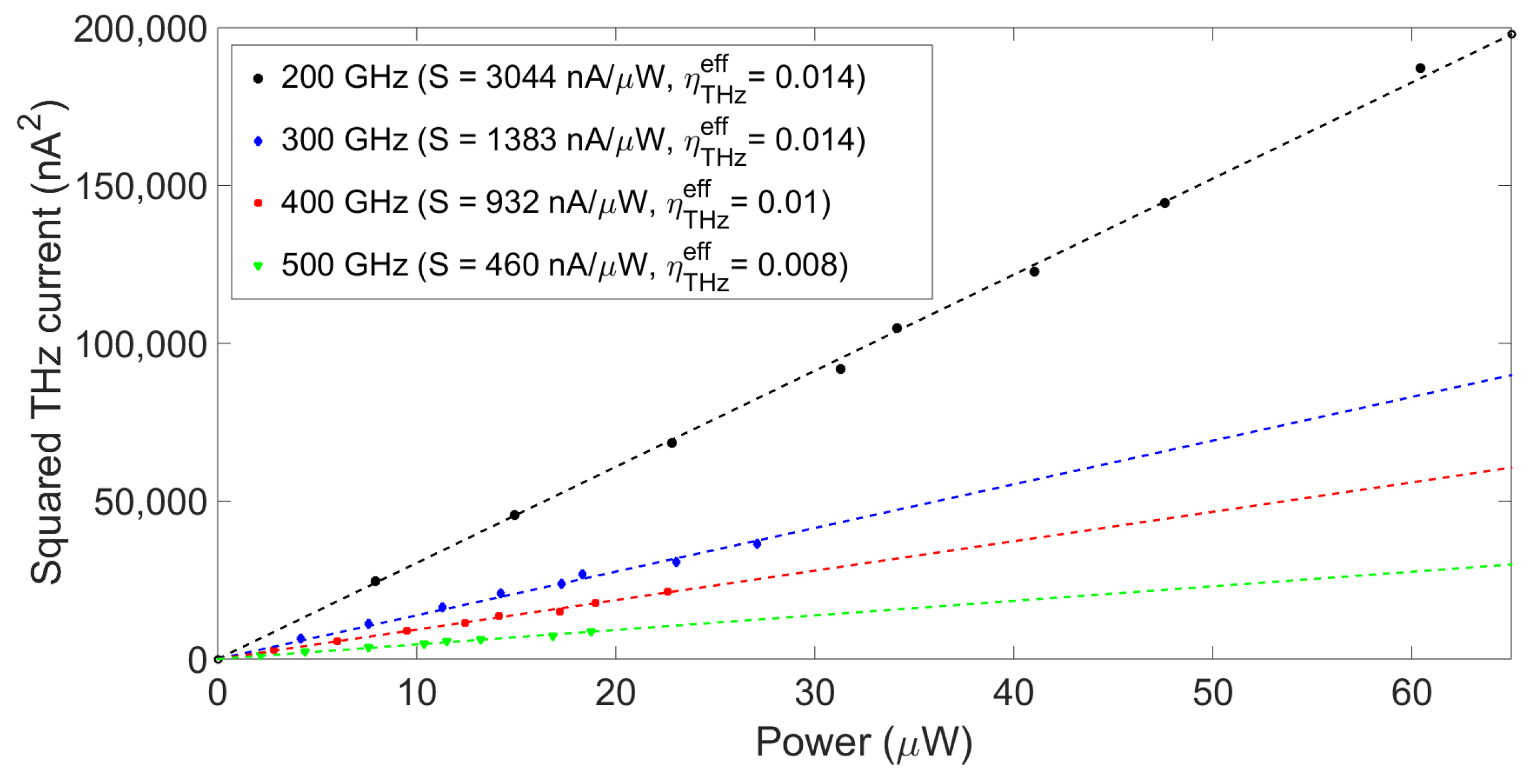
Section 2, the effective terahertz efficiency
was obtained from the experimentally obtained responsivity
for four different frequencies via linear fitting, as shown in
Figure 4. The fitted values were then evaluated using Equation (
10) in order to get four different values of
(one for each frequency). The four obtained values of
were then averaged to get a final value given that they did not vary more than 20%. The measurements for this experimental determination of
were done using only PCA B.
All the parameters required to calcuate
and
, for the whole frequency range of interest, are summarized in
Table 1.
oscillates between the boundaries listed in the table. For the following calculations, the actual frequency-dependent, simulated
is used. The averaged value of
contains the (i) reflection loss of the silicon lens (
), (ii) reflections due to mismatch between the antenna impedance and the silicon wave impedance (
), (iii) mismatch between the THz spot size and the receiving area of the antenna, as well as (iv) differences between DC and AC parameters. The antenna radiation impedance oscillates around 80
, slightly below the wave impedance of silicon. At a point of impedance-matching (
), we estimate the total losses of (i)–(iii) to be in the range of a factor of
. With the definition of
, the AC mobility and THz non-idealities are about five to six times worse than under DC conditions.
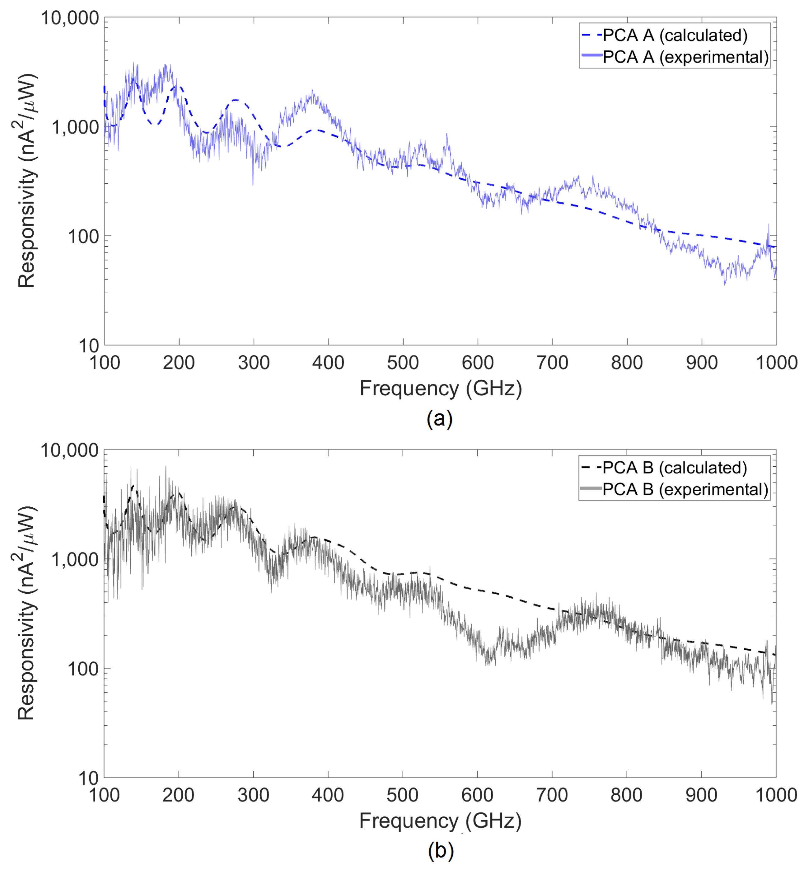
The experimentally obtained responsivity,
, and the calculated one using Equation (
10) and the parameters from
Table 1 are shown in
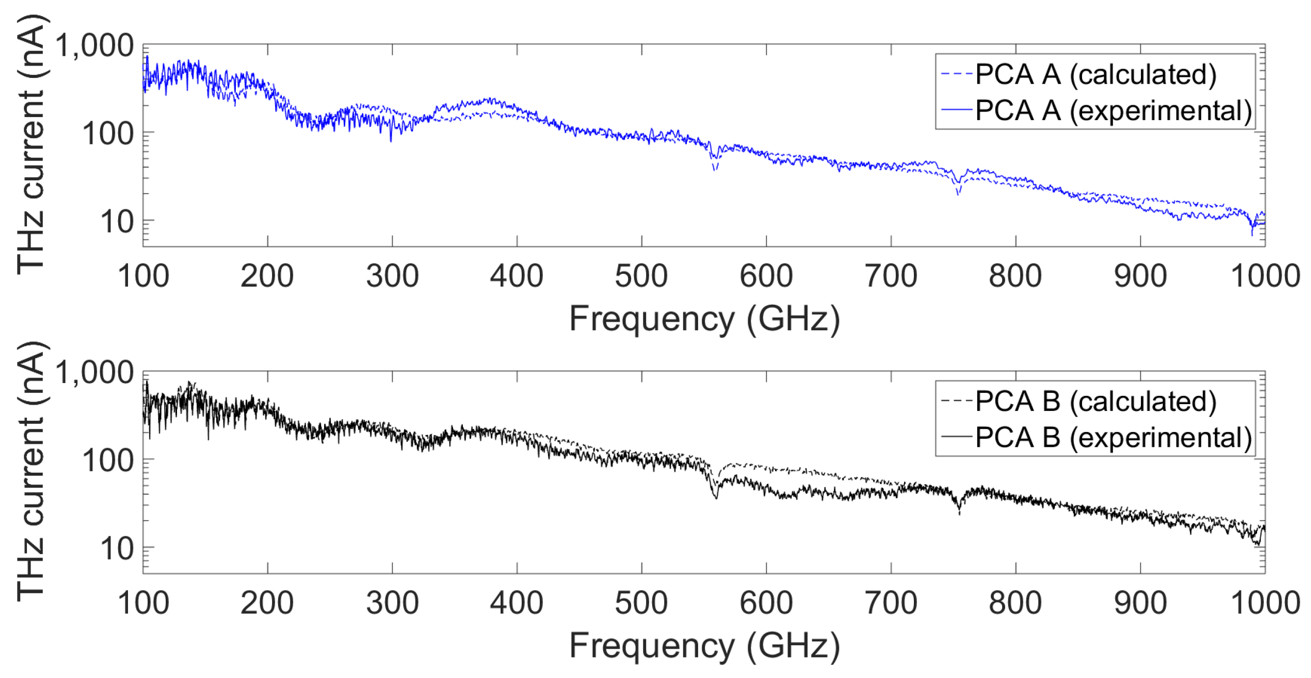
Figure 5 for PCA A and B. The actual measured THz powers and currents used for the determination of the experimental responsivity can be found in
Appendix A.
The agreement between the calculated and the experimentally obtained responsivity is excellent for both PCAs for the whole examined frequency range, using only one parameter extracted from the experimental data of PCA B, namely
. This shows that the theoretical model presented in
Section 2 accurately describes the rectified current for a given incident THz power.
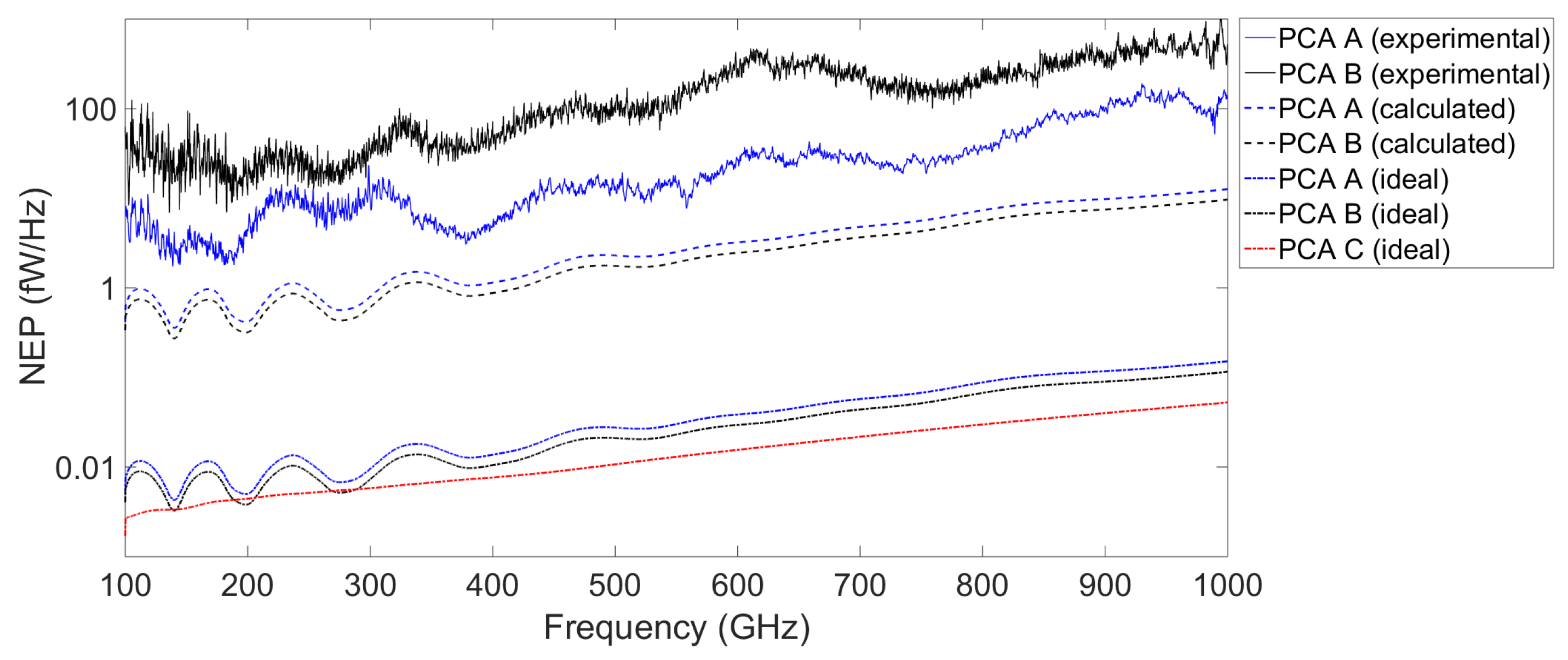
While a photoconductor is actually a mixer, it does not need any external THz local oscillator source as opposed to other THz mixer detectors like Schottky diodes, superconductor–insulator–superconductor (SIS) tunnel junctions, or hot electron-bolometers (HEBs). They can therefore be used as THz power detectors, however, with amplitude and phase sensitivity. For determination of the NEP as defined by Equation (
11), the noise current density,
, has been recorded with laser power but without any THz power incident on the receivers. It is summarized, together with the thermally limited noise current,
, in
Table 1. For all samples, the theoretical noise current is lower than the experimental values, by a factor of 2.6, 6.2 and 4.9 for PCA A, B, and C, respectively. The theoretical NEP represents the lowest limit in a perfect detection chain. In the experimental setup, however, further noise sources are present. Both the transimpedance amplifier (TIA) and the lock-in amplifier add noise. In [
14], the noise floor of the same model of TIA and post detection circuit was determined to 1.45 pA/
(1.9 pA for a detection bandwidth of 1.67 Hz). Further, incoupling of external noise sources by stray fields with frequency components at the modulation frequency increase the noise floor. Last but not least, the NEP calculation neglects laser noise which, in turn, modulates
and thus increases the noise floor. Therefore, the experimental NEPs of PCA A and B are by a factor of
and
higher than the thermal limit, in agreement with the experimental findings shown in
Figure 6, where the calculated NEP assumed the thermally limited noise current and the calculated responsivity shown by the dashed lines in
Figure 5. The lowest measured NEP of 1.81 fW/Hz was achieved with PCA A at 188.8 GHz. For a detection bandwidth of 1 Hz, this value is about five orders of magnitude smaller than the NEP of a Golay cell (direct detection NEP ∼ 150 pW/
) and about three orders of magnitude lower than values reported for Schottky diodes (direct detection NEP ∼ 1.5–20 pW/
at 200 GHz [
20,
21,
22], where some of them are hollow waveguide-coupled devices with excellent noise shielding).
A comparison of the performance between the ErAs:InGaAs PCAs and other THz mixers (e.g., SIS junctions, Schottky diodes or HEBs) in terms of noise equivalent temperature difference (NETD) would require a different set of measurements, i.e., using non-coherent, broadband hot and cold loads as sources [
23]. The goal here was a characterizatio of PCAs as coherent detectors.
Finally, we also estimate the lowest possible NEP for the three PCAs by allowing the AC transport to approximate the DC performance, considering a perfect THz coupling (
), and assuming a noise floor limited only by thermal noise. At 200 GHz, such ideal devices would result in NEPs of 4.2 aW/Hz, 3.3 aW/Hz, and 3.3 aW/Hz for PCA A, B and C, respectively. For the rest of the frequency range the ideal peformance is shown in
Figure 6.


