1. Introduction
Semiconductor lasers emitting a mid-infrared (MIR) range of 2–3 μm find promising applications in gas sensing and detection based on laser spectroscopy. Two common gain media for these lasers are type-I quantum wells (QWs) grown on GaSb substrates as well as type-II QWs grown on InP substrates, excluding cascaded configurations of interband or intraband transitions [
1,
2,
3,
4,
5]. However, GaSb-based type-I QW lasers, which consist of complex quaternary or quinary compounds, are subjected to critical growth parameters and low thermal stability of crystalline [
3]. InP-based type-II QW lasers, on the other hand, benefit from stable growth of ternary alloys and reliable process technology. Since optical gain may diminish because of a spatially indirect recombination in type-II heterostructures, ‘M’-type and ‘W’-type QWs are devised to enhance electron-hole wavefunction overlap [
4,
5].
For the application in tunable diode laser absorption spectroscopy (TDLAS), MIR lasers have to meet the key requirement of single spectral mode. Conventional edge-emitting lasers (EELs), which exhibit mutli-longitudinal-mode emissions, combine external-cavity grating to achieve single-mode operation. GaSb-based external-cavity lasers (ECLs) operating around 2.13 μm were one of the examples [
6]. The standard approach toward single-mode emissions is the introduction of Bragg gratings or one-dimensional (1D) photonic-crystal (PC) gratings beside or atop laser waveguides to yield distributed feedback (DFB) lasers. GaSb-based DFB lasers covering the wavelength range of 1.8–3.0 μm were therefore demonstrated with lateral metal grating [
2]. To facilitate surface emission, advanced vertical-cavity surface-emitting lasers (VCSELs) exhibit single-mode emissions by monolithic incorporation of distributed Bragg reflectors (DBRs) or 1D-PC reflectors. For example, MIR VCSELs based on GaSb and InP substrates demonstrated a single-mode operation with a side-mode suppression ratio (SMSR) over 25 dB at a wavelength range of 2.5–2.6 μm [
7,
8].
Recently, novel photonic-crystal surface-emitting lasers (PCSELs) draw increasing attention because of their single-mode operation, high optical output, and narrow beam divergence [
9,
10,
11,
12]. Based on the band-edge effect of two-dimensional (2D) PCs, light emissions from gain media strongly couple with PC structure to construct 2D cavity mode where in-plane multi-directional distributed feedback (DFB) diffracts vertically. PCSELs have advantages over VCSELs in terms of epitaxial complexity and thickness. These advantages become more obvious in immature material systems and very long emission wavelengths. A clear example is GaSb-based PCSELs of 2.3-μm wavelength range [
10]. Although electrical injection of MIR PCSELs is not yet realized, it can be expected soon with the dawning demonstration of electrically injected near-infrared (NIR) PCSELs [
11,
12]. In this work, we report the first InP-based MIR PCSELs by optical pumping at and above room-temperature (RT). Gain media of InGaAs/GaAsSb ‘W’-type QWs exhibit emission wavelength range of 2.2 μm. Moreover, lasing characteristics of MIR PCSELs of similar wavelength range are compared for both InP- and GaSb-based material systems [
13].
2. Materials and Methods
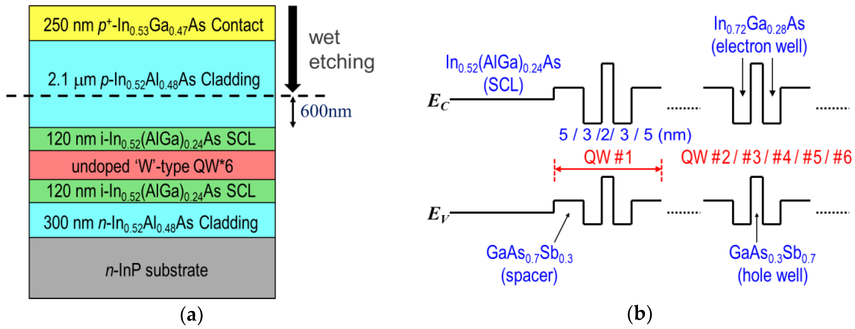
Our investigated sample was grown on S-doped (001) InP substrate by a Veeco GEN II solid source molecular beam epitaxy system. The layer structure (exclusive of active region) and growth conditions were exactly the same as that previously described in Ref. [
5]. The schematic structure is shown in
Figure 1a, and band diagram of active region is shown in
Figure 1b. Quaternary In
0.52(AlGa)
0.24As was used as the separate-confinement layer (SCL). The active region was composed of 6-period ‘W’-type QWs. Each period consisted of GaAs
0.7Sb
0.3/In
0.72Ga
0.28As/GaAs
0.3Sb
0.7/In
0.72Ga
0.28As/GaAs
0.7Sb
0.3 layers in sequence of 5/3/2/3/5 nm. The central layer of GaAs
0.3Sb
0.7 was hole well, and inner two layers of In
0.72Ga
0.28As were electron wells, while outermost GaAs
0.7Sb
0.3 layers were spacers.
Before PC fabrication, top contact layer and part of top cladding layer were removed by the chemical mixture of sulfuric acid, hydrogen peroxide, and de-ionized water. The cladding thickness remained was about 600 nm. Square-lattice PCs for transverse electric polarization were designed to operate around the Γ band-edge. We used e-beam lithography and inductively coupled plasma (ICP) etcher to pattern circular-air-hole PCs on dielectric Si3N4, which was deposited as a hard mask in thickness of 150 nm by plasma enhanced chemical vapor deposition. Again, 2D-PC structure was transferred into semiconductor layers by ICP. To estimate the etch depth of the PC holes, 1D waveguide simulation was performed to obtain a fundamental mode distribution in the vertical direction of PCSEL. At an etch depth around 500 nm, we have an intensity overlap within the PC region of over 5%.
We patterned a series of lattice periods (
p), tested a few etch depths (
d), and varied the air-hole filling factors (
FF, which is defined as air-hole area divided by squared period). The fabricated devices, each with a size of 200 × 200 μm
2, were temperature controlled by a thermoelectric cooler and optically pumped by a 1064-nm pulsed fiber laser. Pulsed optical pumping was operated in a width of 50 ns and repetition rate of 5 KHz. The emitted light was collected with a grating monochromator and an InGaAsSb detector. Resolution as low as 0.05 nm was used in measuring lasing spectra.
Table 1 lists six PCSEL devices as well as their PC parameters. Three lattice periods of 680, 690, and 700 nm are designated as devices A, B, and C, respectively. The lattice periods and filling factors were as-designed values, while depths of PC holes were characterized by scanning electron microscopy (SEM).
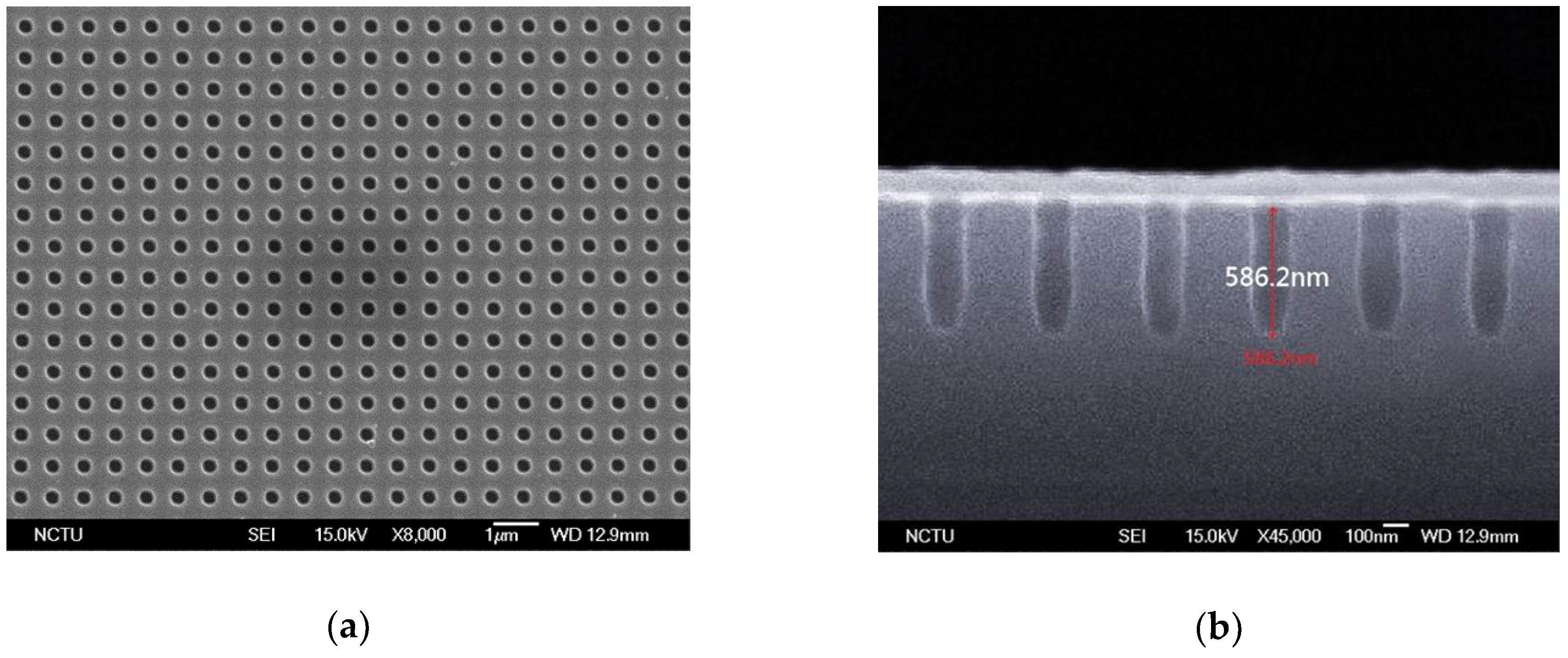
Figure 2 shows the top view and cross-sectional view SEM images of one MIR PCSEL.
3. Results and Discussions
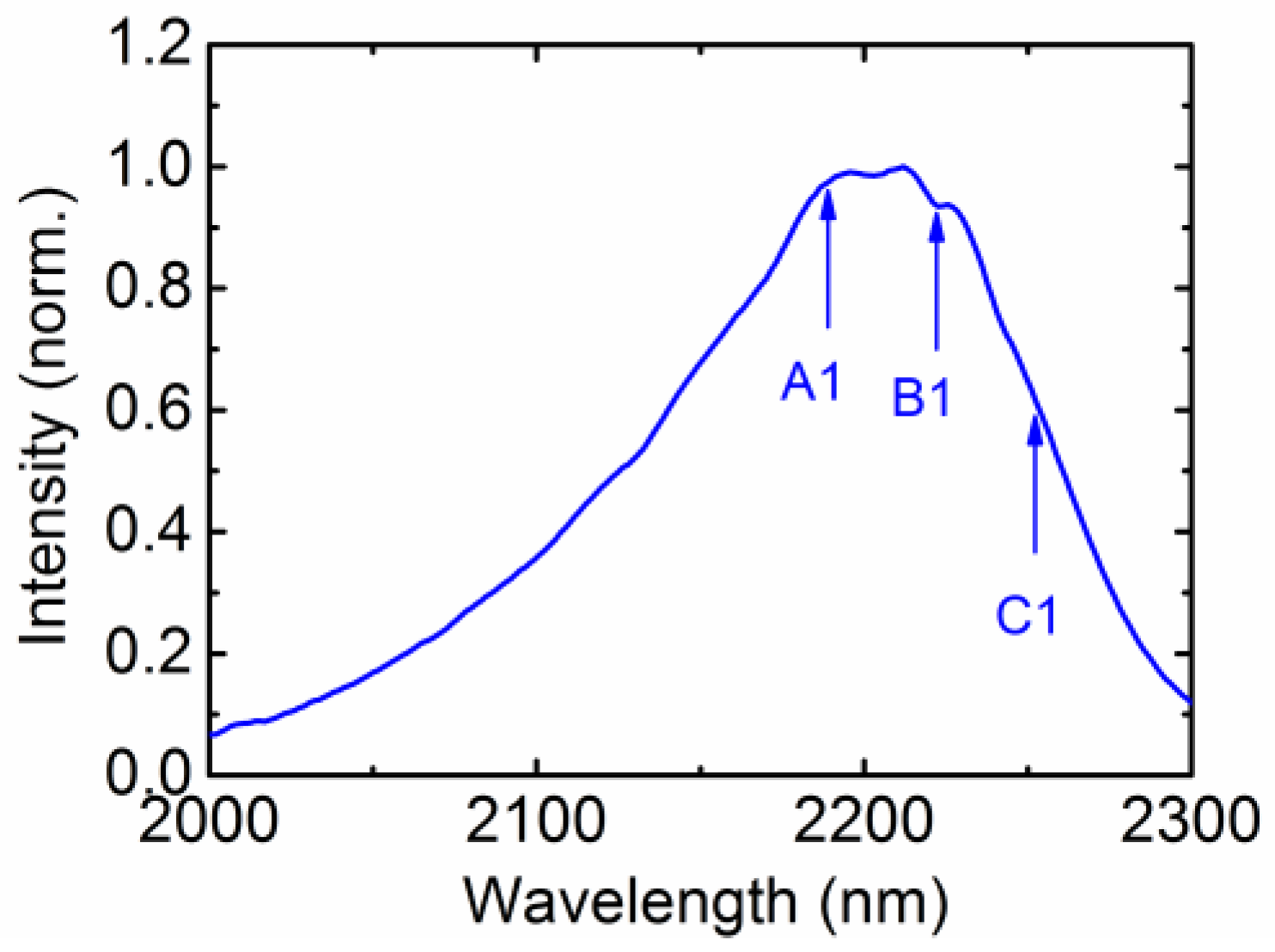
Figure 3 shows the RT photo-luminescence (PL) spectrum of the investigated sample pumped by a 532-nm diode laser. Three arrows are marked in the figure for afterward discussion. The spectral width at 98% intensity was as large as 27 nm (from 2189.5 nm to 2216.5 nm), while the full width at half maximum (FWHM) was about 135 nm (from 2125 nm to 2260 nm). The gain peak of ‘W’-type QW structure (λ
QW) was determined to be 2203 nm by taking the median wavelength of 98% intensity. As regards the RT-PL of GaSb-based type-I QW structure in Ref. [
13], the spectral width at 98% intensity was 10 nm whereas the FWHM was about 121 nm. The flat-top feature in RT-PL is characteristic of InP-based ‘W’-type QWs.
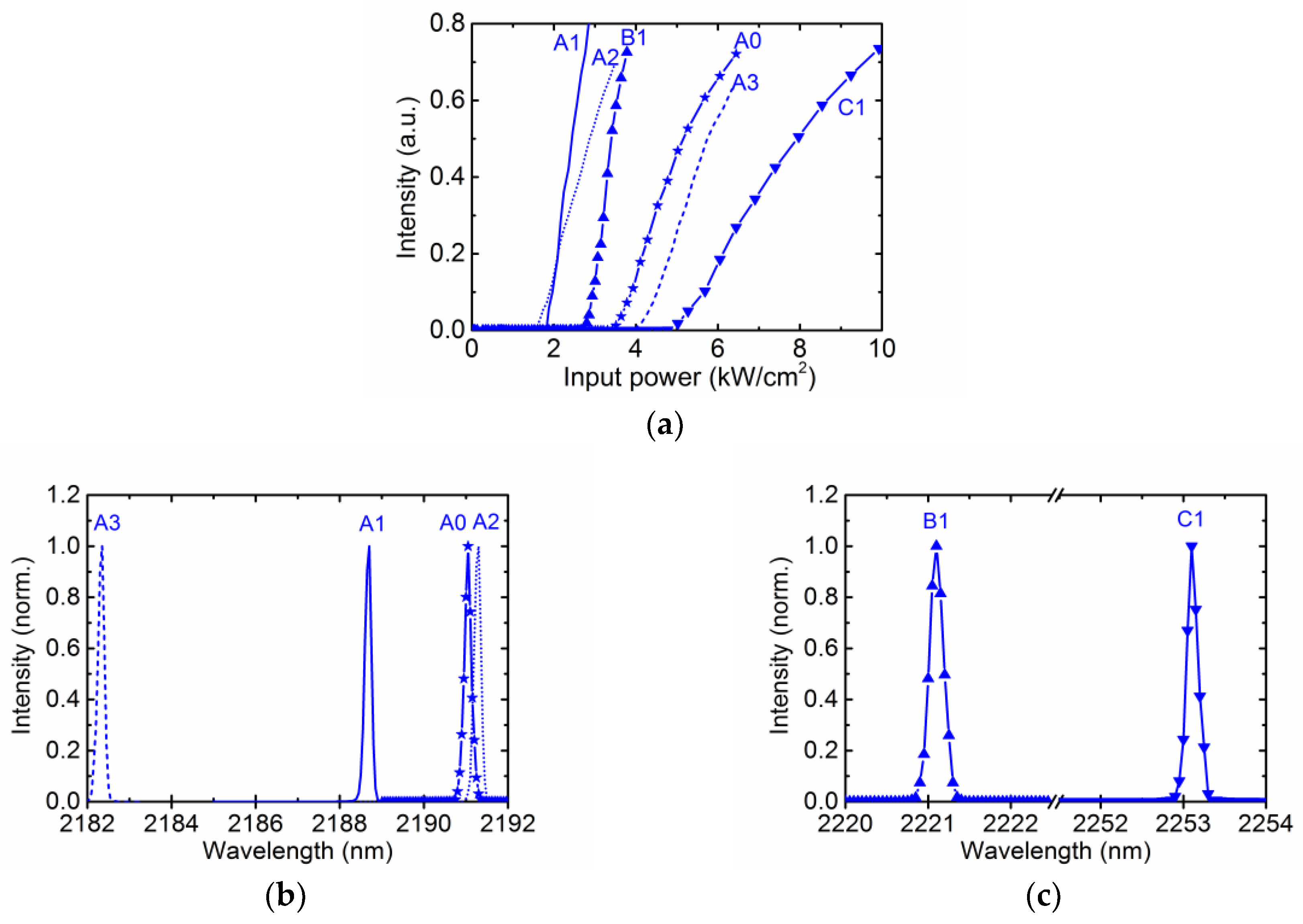
We selected six PCSEL devices with corresponding parameters listed in
Table 1 and analyzed their device characteristics of lasing wavelengths and threshold current densities. Slope efficiencies were not discussed as they may suffer from large deviation among measurements. These PCSELs are investigated in terms of lattice periods (A1, B1 and C1), etch depths (A0 and A1), and filling factors (A1, A2 and A3).
Figure 4 shows the lasing characteristics of light-in versus light-out (
L-L) and the normalized emission spectra for six PCSEL devices at 20 °C. As shown in
Figure 4b,c, lasing wavelengths of PCSEL devices are a function of lattice period, etch depth, and FF.
The effect of lattice period is revealed by device A1, B1, and C1 with respective lasing wavelengths of 2188.7, 2221.1, and 2253.1 nm. The wavelength shift is proportional to period change with factor of 3.2; i.e., 3.2 nm red-shifts in wavelength per nm increase in period. All lasing linewidths are around 0.2 nm, which is much smaller than those of edge emitting lasers [
5]. The nearly single-wavelength lasing emissions are attributed to wavelength selection mechanism of multi-directional DFB effect [
9]. In
Figure 4a, the threshold power densities are about 1.72, 2.68 and 5.02 kW/cm
2 for device A1, B1 and C1, respectively. That increasing threshold power density with increasing lattice period is attributed to gain-cavity detuning (Δλ), which is defined by difference between gain peak of QWs (λ
QW = 2203 nm) and resonant cavity wavelength of PC (λ
PC); i.e., Δλ ≡ λ
QW − λ
PC. Referring to the three arrows marked in
Figure 3, device A1 is positively detuned with the smallest magnitude of 14.3 nm, while device B1 and C1 are negatively detuned with magnitudes of 18.1 nm and 50.1 nm, respectively. The largest detuning magnitude is associated with the lowest material gain, which results in the highest threshold power density.
The effect of etch depth is disclosed by device A0 and A1. Because their wavelength difference is small and stronger, and distributed feedback coupling is associated with deeper PC holes, the pumping threshold of A1 is less than half that of A0. Theoretical investigation on square-lattice-type PCSELs with InGaAs/GaAs MQWs revealed that optimized FF was 0.08 [
14]. In our experiment, FF of 0.05, 0.10, and 0.15 were designed around this theoretical value and embodied in device A2, A1, and A3, respectively. The threshold power density of A3 is the highest among three devices and is partly credited to its large gain-cavity detuning of +20.7 nm. The threshold values of A1 and A2 are within uncertainty; however, their relative relation is consistent for counterparts with 690-nm period, which are not shown here. The lasing characteristics of investigated PCSELs are summarized in
Table 2.
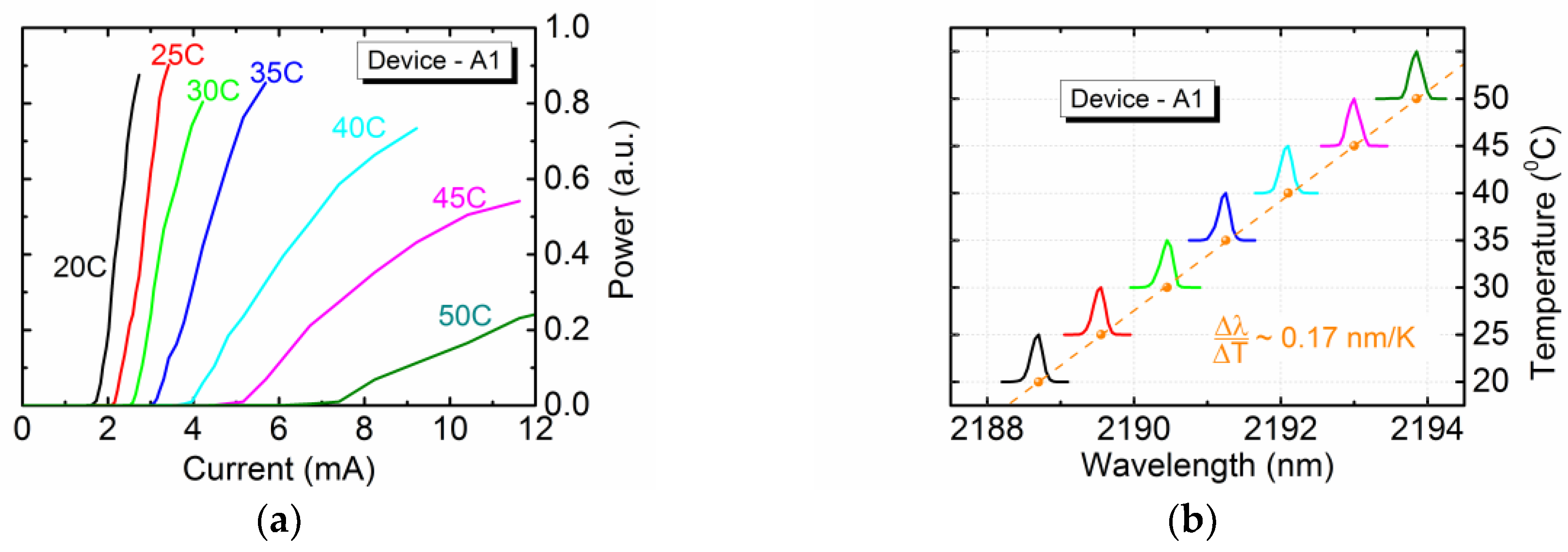
Figure 5a shows the
L-L curves of device A1 at heatsink temperature of 20–50 °C in step of 5 °C. The near-threshold lasing spectra, normalized in linear scale, and shifted in vertical axis, are shown in
Figure 5b. The lasing linewidths are about 0.2 nm at all temperature range. Moreover, peak lasing wavelength shifted with temperature at a rate of 0.17 nm/K, which is about one-seventh to one-sixth smaller than gain-peak shift rate of 1.0–1.2 nm/K (or 0.25–0.3 meV/K) [
8,
15]. The resonance shift of PC cavity dominates over bandgap shrinkage of ‘W’-type QWs in temperature-dependent lasing wavelengths. It is worth it to mention that the temperature shift coefficients of cavity resonance and gain peak for GaSb-based type-I QW PCSELs in similar wavelength range were about 0.2 nm/K and 1.62 nm/K, respectively [
10,
13]. InP-based ‘W’-type QW PCSELs exhibit cavity shift rate 15% lower and gain-peak shift rate about 30% lower than GaSb-based type-I QW PCSELs.
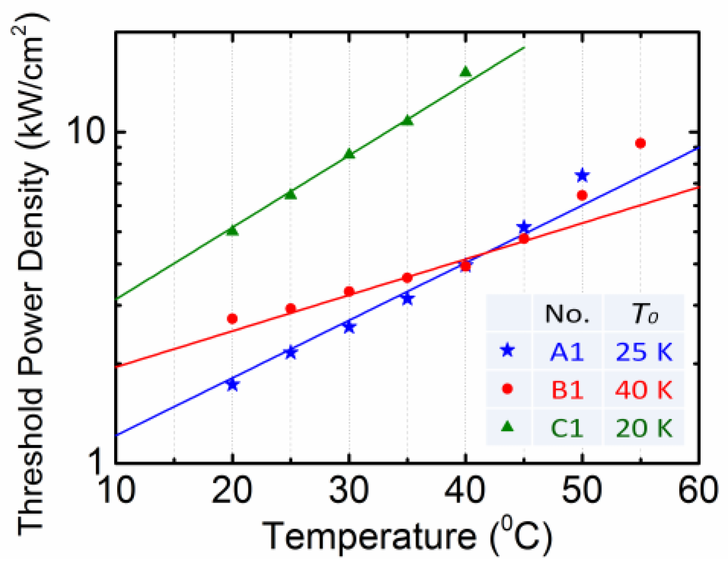
We also measure temperature-dependent lasing characteristics of device B1 and C1. They exhibit a consistent lasing peak shift rate of 0.17 nm/K. The threshold power density as a function of temperature for three PCSELs is plotted in
Figure 6. At a temperature range below 45 °C, the extracted characteristic temperature (
To) is about 25 K, 40 K and 20 K for device A1, B1, and C1, respectively. Small
To less than 25 K is typical for ‘W’-type QW edge-emitting lasers and VCSELs [
8,
16]. The highest
To of 40 K for device B1 is due to its slightly large negative detuning of 18.1 nm at 20 °C. Zero detuning is estimated to be achieved at 40 °C; however, neither lowest threshold power density nor negative
To is observed around this temperature [
16]. This is possibly due to that device B1 is outside the flat-top region and in the long-wavelength side of PL spectrum. The associated material gain is not high; besides, temperature-induced gain decrement dominates over detuning-induced gain increment. Higher
To can be expected with smaller negative detuning of 10-16 nm based on our previous work of QD PCSELs in NIR range [
17]. For device C1 with largest negative detuning of 50.1 nm at 20 °C, its threshold power density at RT is the highest among three devices as a result of insufficient material gain at around the upper FWHM wavelength of PL spectrum. Since higher pumping density is more sensitive to Auger recombination and carrier loss at elevated temperature, lowest
To is observed for device C1. It is worth mentioning that lasing wavelengths cover more than 70 nm, ranging from 2182 nm to 2253 nm. Moreover, the threshold pumping density is more sensitive to temperature change in InP-based ‘W’-type QW PCSELs (
To = 20–40 K) than in GaSb-based type-I QW PCSELs (
To = 45–67 K, which was revealed in Ref. [
13]).
4. Conclusions
In this paper, InP-based ‘W’-type QW PCSELs in a wavelength range of 2.2 μm are demonstrated for the first time by optical pumping. The lasing emissions show a broad wavelength range over 70 nm and narrow linewidths of about 0.2 nm, which is promising for TDLAS applications. We have investigated lasing characteristics of PCSELs in terms of etch depth, lattice period, and filling factor. The temperature characteristics are also discussed with respect to wavelength detuning between QW gain peak and PC resonant wavelength. Moreover, InP-based ‘W’-type QW gain media and PCSELs exhibit rather flat but lower gain, smaller temperature shift coefficients of cavity resonance and gain peak, as well as lower characteristics temperature in comparison with GaSb-based type-I gain media and PCSELs.
MIR PCSELs can be electrically pumped if the layer structure is suitably designed and ohmic contact is cleverly achieved. In our current injected NIR PCSELs [
11], we deposited transparent contact indium-tin-oxide (ITO) to facilitate both electrical current spreading as well as optical light transmission. However, PC holes of MIR PCSELs are too large and have to be refilled with SU-8 photoresist before ITO deposition. Moreover, the InGaAs contact layer well as ITO could have significant absorption and should be taken care of. The last choice is to use the current injection scheme of the buried tunnel junction commonly used in MIR VCSELs [
7,
8]; nonetheless, epitaxial regrowth is necessary.


