Femtosecond Laser Microfabrication of Artificial Compound Eyes


Abstract
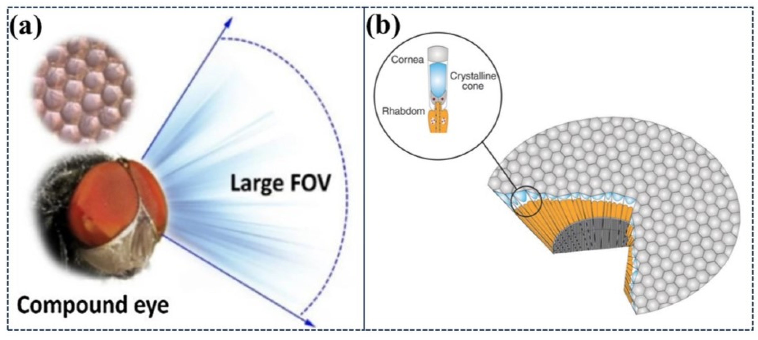
:1. Introduction
2. Femtosecond Laser Processing Technology
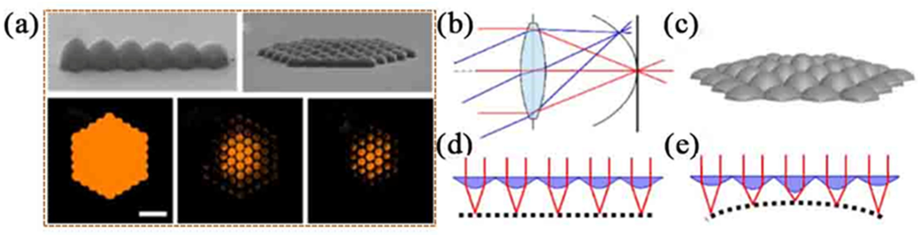
2.1. Two-Photon Polymerization Technology
2.2. Femtosecond Laser Ablation Processing Technology
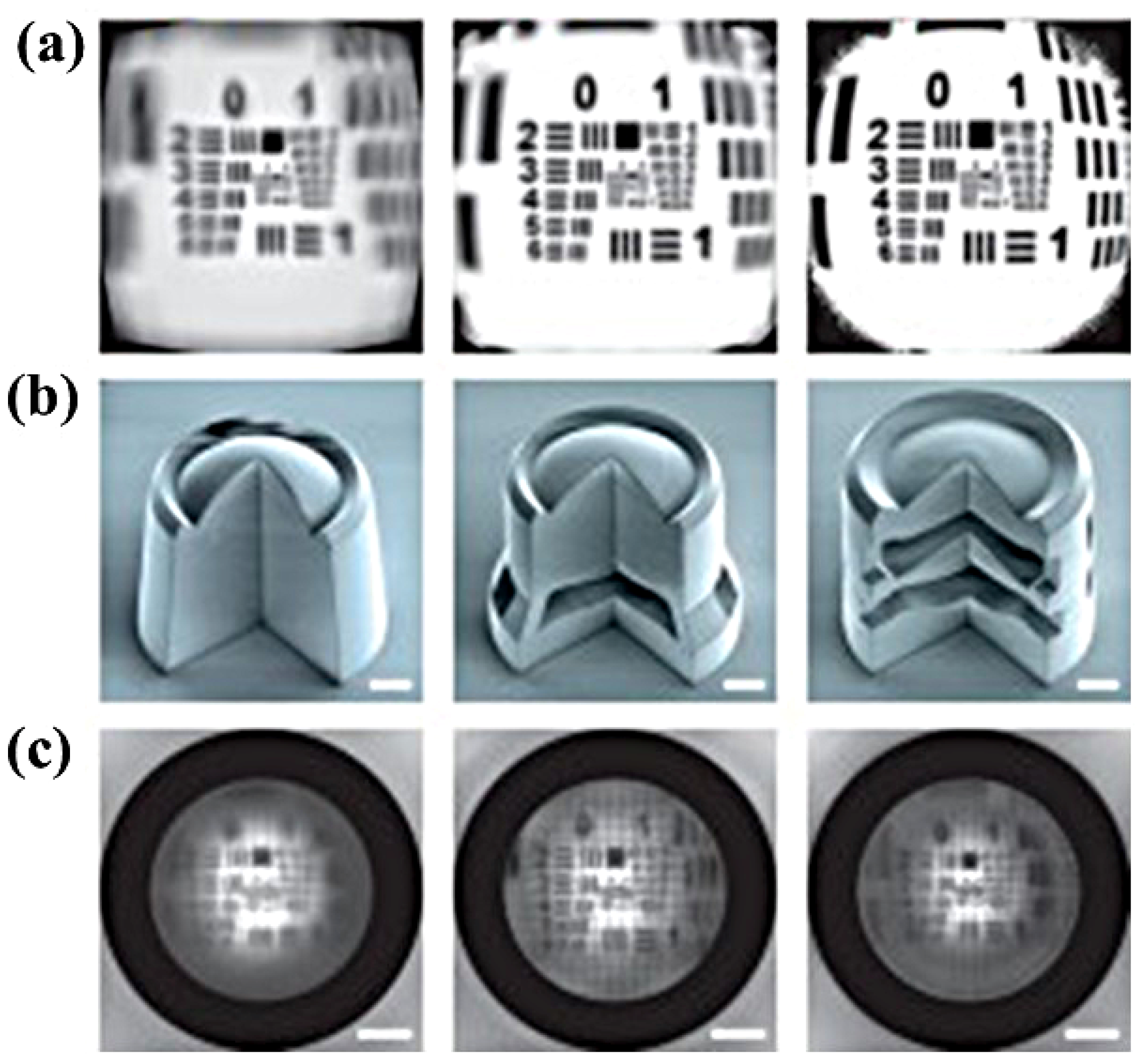
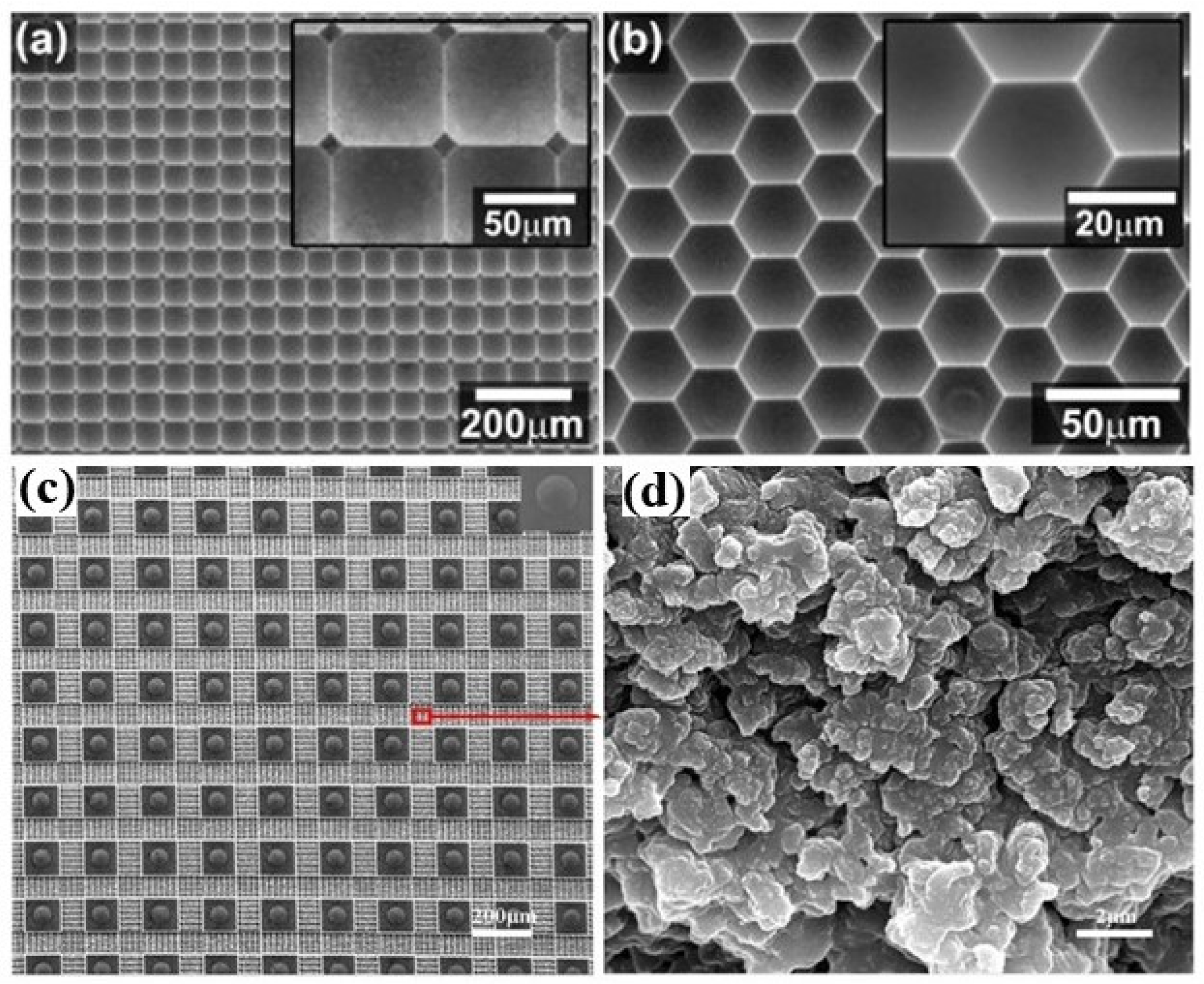
2.2.1. Femtosecond Laser Direct Writing Technology
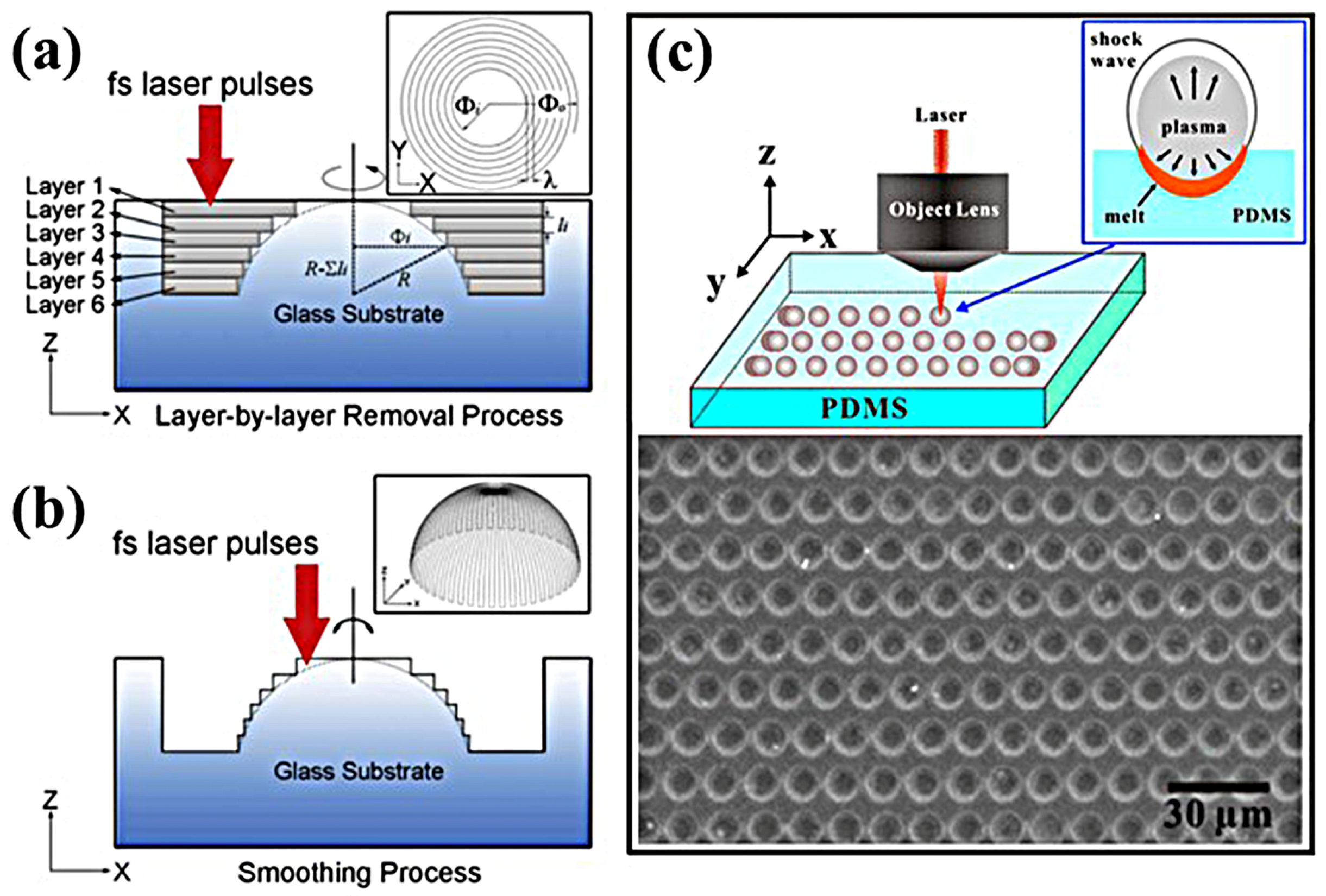
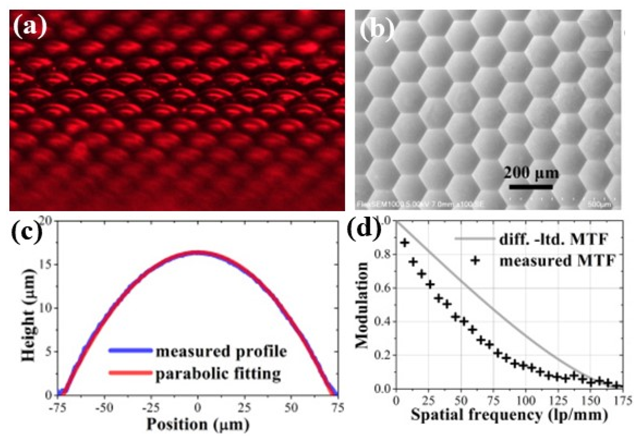
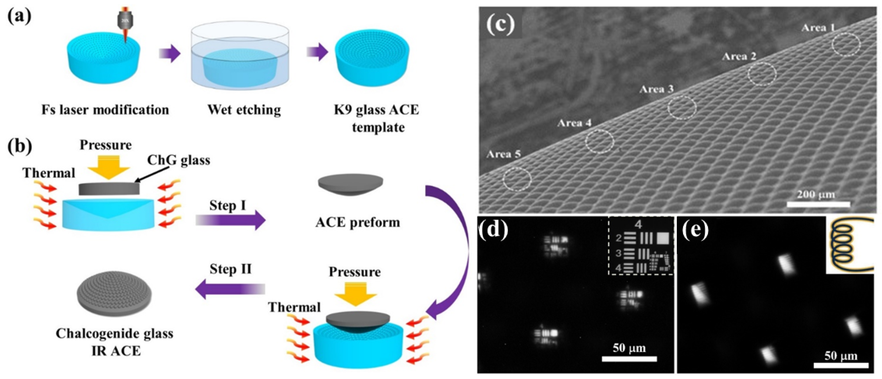
2.2.2. Femtosecond Laser Wet Etching Technology
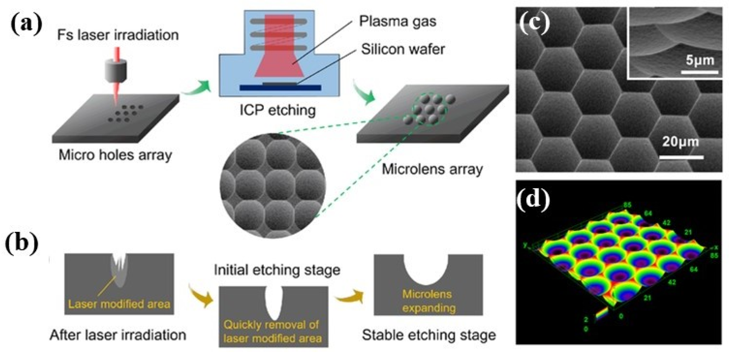
2.2.3. Femtosecond Laser Dry Etching Technology
3. Applications
4. Conclusions
Author Contributions
Funding
Institutional Review Board Statement
Informed Consent Statement
Data Availability Statement
Conflicts of Interest
References
- Cao, J.J.; Hou, Z.S.; Tian, Z.N.; Hua, J.G.; Zhang, Y.L.; Chen, Q.D. Bioinspired zoom compound eyes enable variable-focus imaging. ACS Appl. Mater. Interfaces 2020, 12, 10107–10117. [Google Scholar] [CrossRef]
- Jeong, K.H.; Kim, J.; Lee, L.P. Biologically inspired artificial compound eyes. Science 2006, 312, 557–561. [Google Scholar] [CrossRef]
- Kim, K.; Jang, K.W.; Bae, S.I.; Jeong, K.H. Multi-functional imaging inspired by insect stereopsis. Commun. Eng. 2022, 1, 39. [Google Scholar] [CrossRef]
- Dai, B.; Zhang, L.; Zhao, C.; Bachman, H.; Becker, R.; Mai, J.; Jiao, Z.; Li, W.; Zheng, L.; Wan, X.; et al. Biomimetic apposition compound eye fabricated using microfluidic-assisted 3D printing. Nat. Commun. 2021, 12, 6458. [Google Scholar] [CrossRef]
- Song, Y.M.; Xie, Y.; Malyarchuk, V.; Xiao, J.; Jung, I.; Choi, K.J.; Liu, Z.; Park, H.; Lu, C.; Kim, R.H.; et al. Digital cameras with designs inspired by the arthropod eye. Nature 2013, 497, 95–99. [Google Scholar] [CrossRef]
- Lee, L.P.; Szema, R. Inspirations from biological optics for advanced photonic systems. Science 2005, 310, 1148–1150. [Google Scholar] [CrossRef]
- Duparré, J.W.; Wippermann, F.C. Micro-optical artificial compound eyes. Bioinspir. Biomim. 2006, 1, R1–R16. [Google Scholar] [CrossRef]
- Stavenga, D.; Kinoshita, M.; Yang, E.-C.; Arikawa, K. Retinal regionalization and heterogeneity of butterfly eyes. Sci. Nat. 2001, 88, 477–481. [Google Scholar] [CrossRef] [PubMed]
- Garza-Rivera, A.; Renero-Carrillo, F.-J. Design of artificial apposition compound eye with cylindrical micro-doublets. Opt. Rev. 2011, 18, 184–186. [Google Scholar] [CrossRef]
- Olberg, R.M. Object- and self-movement detectors in the ventral nerve cord of the dragonfly. J. Comp. Physiol. A 1981, 141, 327–334. [Google Scholar] [CrossRef]
- Snyder, A.W.; Stavenga, D.G.; Laughlin, S.B. Spatial information capacity of compound eyes. J. Comp. Physiol. A 1977, 116, 183–207. [Google Scholar] [CrossRef]
- Beersma, D.G.M.; Stavenga, D.G.; Kuiper, J.W. Organization of visual axes in the compound eye of the FlyMusca domestica L. and behavioural consequences. J. Comp. Physiol. A 1975, 102, 305–320. [Google Scholar] [CrossRef]
- Li, J.; Wang, W.; Mei, X.; Pan, A.; Sun, X.; Liu, B.; Cui, J. Artificial compound eyes prepared by a combination of Air-assisted deformation, modified laser swelling, and controlled crystal growth. ACS Nano 2019, 13, 114–124. [Google Scholar] [CrossRef] [PubMed]
- Liang, W.L.; Pan, J.G.; Su, G.D. One-lens camera using a biologically based artificial compound eye with multiple focal lengths. Optica 2019, 6, 326–334. [Google Scholar] [CrossRef]
- Fallah, H.R.; Karimzadeh, A. Design and simulation of a high-resolution superposition compound eye. J. Mod. Opt. 2007, 54, 67–76. [Google Scholar] [CrossRef]
- Fallah, H.R.; Karimzadeh, A. MTF of compound eye. Opt. Express 2010, 18, 12304. [Google Scholar] [CrossRef]
- Gao, X.; Yan, X.; Yao, X.; Xu, L.; Zhang, K.; Zhang, J.; Yang, B.; Jiang, L. The dry-style antifogging properties of mosquito compound eyes and artificial analogues prepared by soft lithography. Adv. Mater. 2007, 19, 2213–2217. [Google Scholar] [CrossRef]
- Sun, Z.; Liao, T.; Liu, K.; Jiang, L.; Kim, J.H.; Dou, S.X. Fly-eye inspired superhydrophobic anti-fogging inorganic nanostructures. Small 2014, 10, 3001–3006. [Google Scholar] [CrossRef]
- Cheng, Y.; Cao, J.; Zhang, F.; Hao, Q. Design and modeling of pulsed-laser three-dimensional imaging system inspired by compound and human hybrid eye. Sci. Rep. 2018, 8, 17164. [Google Scholar] [CrossRef]
- Qu, P.; Chen, F.; Liu, H.; Yang, Q.; Lu, J.; Si, J.; Wang, Y.; Hou, X. A simple route to fabricate artificial compound eye structures. Opt. Express 2012, 20, 5775–5782. [Google Scholar] [CrossRef]
- Huang, C.C.; Wu, X.; Liu, H.; Aldalali, B.; Rogers, J.A.; Jiang, H. Large-Field-of-View Wide-Spectrum Artificial Reflecting Superposition Compound Eyes. Small 2014, 10, 3050–3057. [Google Scholar] [CrossRef] [PubMed]
- Brady, D.J.; Gehm, M.E.; Stack, R.A.; Marks, D.L.; Kittle, D.S.; Golish, D.R.; Vera, E.M.; Feller, S.D. Multiscale gigapixel photography. Nature 2012, 486, 386–389. [Google Scholar] [CrossRef] [PubMed]
- Ko, H.C.; Stoykovich, M.P.; Song, J.; Malyarchuk, V.; Choi, W.M.; Yu, C.-J.; Iii, J.B.G.; Xiao, J.; Wang, S.; Huang, Y.; et al. A hemispherical electronic eye camera based on compressible silicon optoelectronics. Nature 2008, 454, 748–753. [Google Scholar] [CrossRef]
- Zhang, K.; Jung, Y.H.; Mikael, S.; Seo, J.-H.; Kim, M.; Mi, H.; Zhou, H.; Xia, Z.; Zhou, W.; Gong, S.; et al. Origami silicon optoelectronics for hemispherical electronic eye systems. Nat. Commun. 2017, 8, 1782. [Google Scholar] [CrossRef]
- Lee, G.J.; Choi, C.; Kim, D.H.; Song, Y.M. Bioinspired artificial eyes: Optic components, digital cameras, and visual prostheses. Adv. Funct. Mater. 2008, 28, 1705202. [Google Scholar] [CrossRef]
- Iyer, V.; Najafi, A.; James, J.; Fuller, S.; Gollakota, S. Wireless steerable vision for live insects and insect-scale robots. Sci. Robot. 2020, 5, 0839. [Google Scholar] [CrossRef]
- Li, J.; Thiele, S.; Quirk, B.C.; Kirk, R.W.; Verjans, J.W.; Akers, E.; Bursill, C.A.; Nicholls, S.J.; Herkommer, A.M.; Giessen, H.; et al. Ultrathin monolithic 3D printed optical coherence tomography endoscopy for preclinical and clinical use. Light Sci. Appl. 2020, 9, 124. [Google Scholar] [CrossRef]
- Yanny, K.; Antipa, N.; Liberti, W.; Dehaeck, S.; Monakhova, K.; Liu, F.L.; Shen, K.; Ng, R.; Waller, L. Miniscope3D: Optimized single-shot miniature 3D fluorescence microscopy. Light Sci. Appl. 2020, 9, 171. [Google Scholar] [CrossRef]
- Pahlevaninezhad, H.; Khorasaninejad, M.; Huang, Y.-W.; Shi, Z.; Hariri, L.P.; Adams, D.C.; Ding, V.; Zhu, A.; Qiu, C.-W.; Capasso, F.; et al. Nano-optic endoscope for high-resolution optical coherence tomography in vivo. Nat. Photonics 2018, 12, 540–547. [Google Scholar] [CrossRef]
- Lin, R.J.; Su, V.-C.; Wang, S.; Chen, M.K.; Chung, T.L.; Chen, Y.H.; Kuo, H.Y.; Chen, J.-W.; Chen, J.; Huang, Y.-T.; et al. Achromatic metalens array for full-colour light-field imaging. Nat. Nanotechnol. 2019, 14, 227–231. [Google Scholar] [CrossRef] [PubMed]
- Duparré, J.; Dannberg, P.; Schreiber, P.; Bräuer, A.; Tünnermann, A. Thin compound-eye camera. Appl. Opt. 2005, 44, 2949–2956. [Google Scholar] [CrossRef] [PubMed]
- Luo, Y.; Chu, C.H.; Vyas, S.; Kuo, H.Y.; Chia, Y.H.; Chen, M.K.; Shi, X.; Tanaka, T.; Misawa, H.; Huang, Y.-Y.; et al. Varifocal metalens for optical sectioning fluorescence microscopy. Nano Lett. 2021, 21, 5133–5142. [Google Scholar] [CrossRef]
- Holzner, G.; Du, Y.; Cao, X.; Choo, J.; Demello, A.J.; Stavrakis, S. An optofluidic system with integrated microlens arrays for parallel imaging flow cytometry. Lab Chip 2018, 18, 3631–3637. [Google Scholar] [CrossRef]
- Yoshimoto, K.; Yamada, K.; Sasaki, N.; Takeda, M.; Shimizu, S.; Nagakura, T.; Takahashi, H.; Ohno, Y. Evaluation of a compound eye type tactile endoscope. Proc. SPIE 2013, 8575, 81–86. [Google Scholar]
- Ahmed, R.; Yetisen, A.K.; Butt, H. High numerical aperture hexagonal stacked ring-based bidirectional flexible polymer microlens array. ACS Nano 2017, 11, 3155–3165. [Google Scholar] [CrossRef]
- Choi, W.; Shin, R.; Lim, J.; Kang, S. Design methodology for a confocal imaging system using an objective microlens array with an increased working distance. Sci. Rep. 2016, 6, 33278. [Google Scholar] [CrossRef]
- Deng, Z.; Yang, Q.; Chen, F.; Meng, X.; Bian, H.; Yong, J.; Shan, C.; Hou, X. Fabrication of large-area concave microlens array on silicon by femtosecond laser micromachining. Opt. Lett. 2015, 40, 1928–1931. [Google Scholar] [CrossRef]
- Tanida, J.; Kumagai, T.; Yamada, K.; Miyatake, S.; Ishida, K.; Morimoto, T.; Kondou, N.; Miyazaki, D.; Ichioka, Y. Thin observation module by bound optics (TOMBO): An optoelectronic image capturing system. Opt. Comput. 2000, 4089, 1030–1036. [Google Scholar]
- Chen, J.; Lee, H.H.; Wang, D.; Di, S.; Chen, S. Hybrid imprinting process to fabricate a multi-layer compound eye for multispectral imaging. Opt. Express 2017, 25, 4180–4189. [Google Scholar] [CrossRef] [PubMed]
- Huang, C.-C.; Jiang, H. Bio-inspired wide-angle broad-spectrum cylindrical lens based on reflections from micro-mirror array on a cylindrical elastomeric membrane. Micromachines 2014, 5, 373–384. [Google Scholar] [CrossRef]
- Bi, X.; Li, W. Fabrication of flexible microlens arrays through vapor-induced dewetting on selectively plasma-treated surfaces. J. Mater. Chem. C 2015, 3, 5825–5834. [Google Scholar] [CrossRef]
- Choi, H.J.; Kang, E.K.; Ju, G.W.; Song, Y.M.; Lee, Y.T. Shape-controllable, bottom-up fabrication of microlens using oblique angle deposition. Opt. Lett. 2016, 41, 3328–3330. [Google Scholar] [CrossRef] [PubMed]
- Kang, D.; Pang, C.; Kim, S.M.; Cho, H.S.; Um, H.S.; Choi, Y.W.; Suh, K.Y. shape-controllable microlens arrays via direct transfer of photocurable polymer droplets. Adv. Mater. 2012, 24, 1709–1715. [Google Scholar] [CrossRef]
- Lai, L.-J.; Zhou, H.; Zhu, L.-M. Fabrication of microlens array on silicon surface using electrochemical wet stamping technique. Appl. Surf. Sci. 2016, 364, 442–445. [Google Scholar] [CrossRef]
- Surdo, S.; Diaspro, A.; Duocastella, M. Microlens fabrication by replica molding of frozen laser-printed droplets. Appl. Surf. Sci. 2017, 418, 554–558. [Google Scholar] [CrossRef]
- Liu, F.; Bian, H.; Zhang, F.; Yang, Q.; Shan, C.; Li, M.J.; Hou, X.; Chen, F. IR artificial compound eye. Adv. Opt. Mater. 2020, 8, 1901767. [Google Scholar] [CrossRef]
- Bowen, J.J.; Taylor, J.M.; Jurich, C.P.; Morin, S.A. Stretchable chemical patterns for the assembly and manipulation of arrays of microdroplets with lensing and micromixing functionality. Adv. Funct. Mater. 2015, 25, 5520–5528. [Google Scholar] [CrossRef]
- Lee, J.Y.; Hong, B.H.; Kim, W.Y.; Min, S.Y.; Kim, Y.; Jouravlev, M.; Bose, R.; Kim, K.S.; Hwang, I.; Kaufman, F.; et al. Near-field focusing and magnification through self-assembled nanoscale spherical lenses. Nature 2009, 460, 498–501. [Google Scholar] [CrossRef]
- Lu, Y.; Yin, Y.D.; Xia, Y.N. A self-assembly approach to the fabrication of patterned, two-dimensional arrays of microlenses of organic polymers. Adv. Mater. 2001, 13, 34–37. [Google Scholar] [CrossRef]
- Lee, K.; Wagermaier, W.; Masic, A.; Kommareddy, K.P.; Bennet, M.; Manjubala, I.; Lee, S.-W.; Park, S.B.; Cölfen, H.; Fratzl, P. Self-assembly of amorphous calcium carbonate microlens arrays. Nat. Commun. 2012, 3, 725. [Google Scholar] [CrossRef]
- Zhang, D.; Xu, Q.; Fang, C.; Wang, K.; Wang, X.; Zhuang, S.; Dai, B. Fabrication of a microlens array with controlled curvature by thermally curving photosensitive gel film beneath microholes. ACS Appl. Mater. Interfaces 2017, 9, 16604–16609. [Google Scholar] [CrossRef]
- Jung, H.; Jeong, K.-H. Monolithic polymer microlens arrays with high numerical aperture and high packing density. ACS Appl. Mater. Interfaces 2015, 7, 2160–2165. [Google Scholar] [CrossRef] [PubMed]
- Tormen, M.; Carpentiero, A.; Ferrari, E.; Cojoc, D.; Di Fabrizio, E. Novel fabrication method for three-dimensional nanostructuring: An application to micro-optics. Nanotechnology 2007, 18, 385301. [Google Scholar] [CrossRef]
- Chan, E.P.; Crosby, A.J. Fabricating Microlens Arrays by Surface Wrinkling. Adv. Mater. 2006, 18, 3238–3242. [Google Scholar] [CrossRef]
- Jiang, L.; Wang, A.-D.; Li, B.; Cui, T.-H.; Lu, Y.-F. Electrons dynamics control by shaping femtosecond laser pulses in micro/nanofabrication: Modeling, method, measurement and application. Light Sci. Appl. 2018, 7, 17134. [Google Scholar] [CrossRef] [PubMed]
- Bonse, J.; Baudach, S.; Krüger, J.; Kautek, W.; Lenzner, M. Femtosecond laser ablation of silicon–modification thresholds and morphology. Appl. Phys. A 2003, 74, 19–25. [Google Scholar] [CrossRef]
- Matsuo, S.; Hashimoto, S. Spontaneous formation of 10-mum-scale periodic patterns in transverse-scanning femtosecond laser processing. Opt. Express 2015, 23, 165–171. [Google Scholar] [CrossRef] [PubMed]
- Bian, H.; Shan, C.; Liu, K.; Chen, F.; Yang, Q.; Yong, J.; Hou, X. A miniaturized Rogowski current transducer with wide bandwidth and fast response. J. Micromech. Microeng. 2016, 26, 115015. [Google Scholar] [CrossRef]
- Chen, F.; Zhang, D.; Yang, Q.; Yong, J.; Du, G.; Si, J.; Yun, F.; Hou, X. Bioinspired wetting surface via laser microfabrication. ACS Appl. Mater. Interfaces 2013, 5, 6777–6792. [Google Scholar] [CrossRef]
- Lin, J.; Yu, S.; Ma, Y.; Fang, W.; He, F.; Qiao, L.; Tong, L.; Cheng, Y.; Xu, Z. On-chip three-dimensional high-Q microcavities fabricated by femtosecond laser direct writing. Opt. Express 2012, 20, 10212–10217. [Google Scholar] [CrossRef]
- Lu, D.-X.; Zhang, Y.-L.; Han, D.-D.; Wang, H.; Xia, H.; Chen, Q.-D.; Ding, H.; Sun, H.-B. Solvent-tunable PDMS microlens fabricated by femtosecond laser direct writing. J. Mater. Chem. C 2015, 3, 1751–1756. [Google Scholar] [CrossRef]
- Nishiyama, H.; Nishii, J.; Mizoshiri, M.; Hirata, Y. Microlens arrays of high-refractive-index glass fabricated by femtosecond laser lithography. Appl. Surf. Sci. 2009, 255, 9750–9753. [Google Scholar] [CrossRef]
- Sugioka, K.; Xu, J.; Wu, D.; Hanada, Y.; Wang, Z.; Cheng, Y.; Midorikawa, K. Femtosecond laser 3D micromachining: A powerful tool for the fabrication of microfluidic, optofluidic, and electrofluidic devices based on glass. Lab Chip 2014, 14, 3447–3458. [Google Scholar] [CrossRef] [PubMed]
- Zhang, H.; Yang, F.; Dong, J.; Du, L.; Wang, C.; Zhang, J.; Guo, C.F.; Liu, Q. Kaleidoscopic imaging patterns of complex structures fabricated by laser-induced deformation. Nat. Commun. 2016, 7, 13743. [Google Scholar] [CrossRef] [PubMed]
- Zheng, C.; Hu, A.; Kihm, K.D.; Ma, Q.; Li, R.; Chen, T.; Duley, W.W. femtosecond laser fabrication of cavity microball lens (CMBL) inside a PMMA substrate for super-wide angle imaging. Small 2015, 11, 3007–3016. [Google Scholar] [CrossRef]
- Albota, M.; Beljonne, D.; Bredas, J.L.; Ehrlich, J.; Fu, J.; Heikal, A.A.; Hess, S.E.; Kogej, T.; Levin, M.; Marder, S.; et al. Design of organic molecules with large two-photon absorption cross-sections. Science 1998, 281, 1653–1656. [Google Scholar] [CrossRef]
- Kawata, S.; Sun, H.-B.; Tanaka, T.; Takada, K. Finer features for functional microdevices. Nature 2001, 412, 697–698. [Google Scholar] [CrossRef] [PubMed]
- Tanaka, T.; Ishikawa, A.; Kawata, S. Two-photon-induced reduction of metal ions for fabricating three-dimensional electrically conductive metallic microstructure. Appl. Phys. Lett. 2006, 88, 081107. [Google Scholar] [CrossRef]
- Hu, Y.; Chen, Y.; Ma, J.; Li, J.; Huang, W.; Chu, J. High-efficiency fabrication of aspheric microlens arrays by holographic femtosecond laser-induced photopolymerization. Appl. Phys. Lett. 2013, 103, 141112. [Google Scholar] [CrossRef]
- Xu, B.B.; Xia, H.; Niu, L.G.; Zhang., Y.L.; Sun, K.; Chen, Q.D.; Xu, Y.; LV, Z.Q.; Li, Z.H.; Misawa, H.; et al. Flexible nanowiring of metal on nonplanar substrates by femtosecond-laser-induced electroless plating. Small 2010, 6, 1762–1766. [Google Scholar] [CrossRef]
- Cumpston, B.H.; Ananthavel, S.P.; Barlow, S.; Dyer, D.L.; Ehrlich, J.E.; Erskine, L.L.; Heikal, A.A.; Kuebler, S.M.; Lee, I.-Y.S.; McCord-Maughon, D.; et al. Two-photon polymerization initiators for three-dimensional optical data storage and microfabrication. Nature 1999, 398, 51–54. [Google Scholar] [CrossRef]
- Deubel, M.; von Freymann, G.; Wegener, M.; Pereira, S.; Busch, K.; Soukoulis, C.M. Direct laser writing of three-dimensional photonic-crystal templates for telecommunications. Nat. Mater. 2004, 3, 444–447. [Google Scholar] [CrossRef]
- Guo, R.; Xiao, S.; Zhai, X.; Li, J.; Xia, A.; Huang, W. Micro lens fabrication by means of femtosecond two photon photopolymerization. Opt. Express 2006, 14, 810–816. [Google Scholar] [CrossRef]
- Wu, D.; Wu, S.Z.; Niu, L.G.; Chen, Q.D.; Wang, R.; Song, J.F.; Fang, H.H.; Sun, H.B. High numerical aperture microlens arrays of close packing. Appl. Phys. Lett. 2010, 97, 031109. [Google Scholar] [CrossRef]
- Gissibl, T.; Thiele, S.; Herkommer, A.; Giessen, H. Two-photon direct laser writing of ultracompact multi-lens objectives. Nat. Photonics 2016, 10, 554–560. [Google Scholar] [CrossRef]
- Tian, Z.N.; Yao, W.G.; Xu, J.J.; Yu, Y.H.; Chen, Q.D.; Sun, H.B. Focal varying microlens array. Opt. Lett. 2015, 40, 4222–4225. [Google Scholar] [CrossRef] [PubMed]
- Abrahamsson, S.; Chen, J.; Hajj, B.; Stallinga, S.; Katsov, A.Y.; Wisniewski, J.; Mizuguchi, G.; Soule, P.; Mueller, F.; Darzacq, C.D.; et al. Fast multicolor 3D imaging using aberration-corrected multifocus microscopy. Nat. Methods 2013, 10, 60–63. [Google Scholar] [CrossRef]
- Wu, D.; Wang, J.N.; Niu, L.G.; Zhang, X.L.; Wu, S.Z.; Chen, Q.D.; Lee, L.P.; Sun, H.B. Bioinspired fabrication of high-quality 3D artificial compound eyes by voxel-modulation femtosecond laser writing for distortion-free wide-field-of-view imaging. Adv. Opt. Mater. 2014, 2, 751–758. [Google Scholar] [CrossRef]
- Sun, Q.; Juodkazis, S.; Murazawa, N.; Mizeikis, V.; Misawa, H. Freestanding and movable photonic microstructures fabricated by photopolymerization with femtosecond laser pulses. J. Micromech. Microeng. 2010, 20, 035004. [Google Scholar] [CrossRef]
- Prabhakaran, P.; Son, Y.; Ha, C.-W.; Park, J.-J.; Jeon, S.; Lee, K.-S. Optical materials forming tightly polymerized voxels during laser direct writing. Adv. Eng. Mater. 2018, 20, 1800320. [Google Scholar] [CrossRef]
- Ma, Z.C.; Hu, X.Y.; Zhang, Y.L.; Liu, X.Q.; Hou, Z.S.; Niu, L.G.; Zhu, L.; Han, B.; Chen, Q.D.; Sun, H.B. Smart compound eyes enable tunable imaging. Adv. Funct. Mater. 2019, 29, 1903340. [Google Scholar] [CrossRef]
- Wei, S.; Liu, J.; Zhao, Y.; Zhang, T.; Zheng, M.; Jin, F.; Dong, X.; Xing, J.; Duan, X.; Lu, Y. Protein-based 3D microstructures with controllable morphology and pH-responsive properties. ACS Appl. Mater. Interfaces 2017, 9, 42247–42257. [Google Scholar] [CrossRef] [PubMed]
- Lay, C.L.; Lee, Y.H.; Lee, M.R.; Phang, I.Y.; Ling, X.Y. Formulating an ideal protein photoresist for fabricating dynamic microstructures with high aspect ratios and uniform responsiveness. ACS Appl. Mater. Interfaces 2016, 8, 8145–8153. [Google Scholar] [CrossRef] [PubMed]
- Malinauskas, M.; Žukauskas, A.; Hasegawa, S.; Hayasaki, Y.; Mizeikis, V.; Buividas, R.; Juodkazis, S. Ultrafast laser processing of materials: From science to industry. Light Sci. Appl. 2016, 5, 16133. [Google Scholar] [CrossRef]
- Wang, A.; Jiang, L.; Li, X.; Liu, Y.; Dong, X.; Qu, L.; Duan, X.; Lu, Y. Mask-free patterning of high-conductivity metal nanowires in open air by spatially modulated femtosecond laser pulses. Adv. Mater. 2015, 27, 6238–6243. [Google Scholar] [CrossRef]
- Fang, R.; Vorobyev, A.; Guo, C. Direct visualization of the complete evolution of femtosecond laser-induced surface structural dynamics of metals. Light Sci. Appl. 2017, 6, e16256. [Google Scholar] [CrossRef]
- Cao, X.W.; Lu, Y.M.; Fan, H.; Xia, H.; Zhang, L.; Zhang, Y.L. Wet-etching-assisted femtosecond laser holographic processing of a sapphire concave microlens array. Appl. Opt. 2018, 57, 9604–9608. [Google Scholar] [CrossRef] [PubMed]
- Liu, H.; Chen, F.; Wang, X.; Yang, Q.; Zhang, D.; Si, J.; Hou, X. Photoetching of spherical microlenses on glasses using a femtosecond laser. Opt. Commun. 2009, 282, 4119–4123. [Google Scholar] [CrossRef]
- Yong, J.; Chen, F.; Yang, Q.; Du, G.; Bian, H.; Zhang, D.; Si, J.; Yun, F.; Hou, X. Rapid fabrication of large-area concave microlens arrays on PDMS by a femtosecond laser. ACS Appl. Mater. Interfaces 2013, 5, 9382–9385. [Google Scholar] [CrossRef]
- Sugioka, K.; Cheng, Y. Ultrafast lasers—Reliable tools for advanced materials processing. Light Sci. Appl. 2014, 3, e149. [Google Scholar] [CrossRef]
- Ams, M.; Marshall, G.D.; Dekker, P.; Dubov, M.; Mezentsev, V.K.; Bennion, I.; Withford, M.J. Investigation of ultrafast laser-photonic material interactions: Challenges for directly written glass photonics. IEEE J. Sel. Top. Quantum Electron. 2008, 14, 1370–1381. [Google Scholar] [CrossRef]
- Marcinkevičius, A.; Juodkazis, S.; Watanabe, M.; Miwa, M.; Matsuo, S.; Misawa, H.; Nishii, J. Femtosecond laser-assisted three-dimensional microfabrication in silica. Opt. Lett. 2001, 26, 277–279. [Google Scholar] [CrossRef] [PubMed]
- Hnatovsky, C.; Taylor, R.; Simova, E.; Rajeev, P.; Rayner, D.; Bhardwaj, V.; Corkum, P. Fabrication of microchannels in glass using focused femtosecond laser radiation and selective chemical etching. Appl. Phys. A 2006, 84, 47–61. [Google Scholar] [CrossRef]
- Wortmann, D.; Gottmann, J.; Brandt, N.; Horn-Solle, H. Micro- and nanostructures inside sapphire by fs-laser irradiation and selective etching. Opt. Express 2008, 16, 1517–1522. [Google Scholar] [CrossRef]
- Li, X.W.; Xie, Q.; Jiang, L.; Han, W.N.; Wang, Q.S.; Wang, A.D.; Hu, J.; Lu, Y.F. Controllable Si (100) micro/nanostructures by chemical-etching-assisted femtosecond laser single-pulse irradiation. Appl. Phys. Lett. 2017, 110, 181907. [Google Scholar] [CrossRef]
- Liu, H.; Chen, F.; Yang, Q.; Qu, P.; He, S.; Wang, X.; Si, J.; Hou, X. Fabrication of bioinspired omnidirectional and gapless microlens array for wide field-of-view detections. Appl. Phys. Lett. 2012, 100, 133701. [Google Scholar] [CrossRef]
- Meng, X.; Chen, F.; Yang, Q.; Bian, H.; Liu, H.; Qu, P.; Hu, Y.; Si, J.; Hou, X. A simple way to fabricate close-packed high numerical aperture microlens arrays. IEEE Photonics Technol. Lett. 2013, 25, 1336–1339. [Google Scholar] [CrossRef]
- Zhang, F.; Yang, Q.; Bian, H.; Liu, F.; Li, M.; Hou, X.; Chen, F. Fabrication of ZnSe microlens array for a wide infrared spectral region. IEEE Photonics Technol. Lett. 2020, 32, 1327–1330. [Google Scholar] [CrossRef]
- Hu, Y.L.; Rao, S.L.; Wu, S.Z.; Wei, P.F.; Qiu, W.X.; Wu, D.; Xu, B.; Ni, J.; Yang, L.; Li, J.; et al. All-Glass 3D optofluidic microchip with built-in tunable microlens fabricated by femtosecond laser-assisted etching. Adv. Opt. Mater. 2018, 6, 1701299. [Google Scholar] [CrossRef]
- Chen, F.; Liu, H.; Yang, Q.; Wang, X.; Hou, C.; Bian, H.; Liang, W.; Si, J.; Hou, X. Maskless fabrication of concave microlens arrays on silica glasses by a femtosecond-laser-enhanced local wet etching method. . Opt. Express 2010, 18, 20334–20343. [Google Scholar] [CrossRef]
- Huang, Q.; Yin, K.; Wang, L.; Deng, Q.; Arnusch, C.J. Femtosecond laser-scribed superhydrophilic/superhydrophobic self-splitting patterns for one droplet multi-detection. Nanoscale 2023, 15, 11247–11254. [Google Scholar] [CrossRef]
- Pei, J.; Yin, K.; Wu, T.; Wang, L.; Deng, Q.; Huang, Y.; Wang, K.; Arnusch, C.J. Multifunctional polyimide-based femtosecond laser micro/nanostructured films with triple Janus properties. Nanoscale 2023, 15, 15708–15716. [Google Scholar] [CrossRef] [PubMed]
- Li, M.; Yang, Q.; Chen, F.; Yong, J.; Bian, H.; Wei, Y.; Fang, Y.; Hou, X. Integration of great water repellence and imaging performance on a superhydrophobic pdms microlens array by femtosecond laser microfabrication. Adv. Eng. Mater. 2019, 21, 1800994. [Google Scholar] [CrossRef]
- Yong, J.; Yang, Q.; Hou, X.; Chen, F. Nature-inspired superwettability achieved by femtosecond lasers. Ultrafast Sci. 2022, 2022, 9895418. [Google Scholar] [CrossRef]
- Zhang, D.; Chen, F.; Yang, Q.; Si, J.; Hou, X. Mutual wetting transition between isotropic and anisotropic on directional structures fabricated by femotosecond laser. Soft Matter 2011, 7, 8337–8342. [Google Scholar] [CrossRef]
- Yong, J.; Singh, S.C.; Zhan, Z.; Chen, F.; Guo, C. How To obtain six different superwettabilities on a same microstructured pattern: Relationship between various superwettabilities in different solid/liquid/gas systems. Langmuir 2019, 35, 921–927. [Google Scholar] [CrossRef] [PubMed]
- Yong, J.; Zhang, C.; Bai, X.; Zhang, J.; Yang, Q.; Hou, X.; Chen, F. Designing “supermetalphobic” surfaces that greatly repel liquid metal by femtosecond laser processing: Does the surface chemistry or microstructure play a crucial role? Adv. Mater. Interfaces 2020, 7, 1901931. [Google Scholar] [CrossRef]
- Deng, Z.F.; Chen, F.; Yang, Q.; Bian, H.; Du, G.; Yong, J.; Hou, X. Dragonfly-eye-inspired artificial compound eyes with sophisticated imaging. Adv. Funct. Mater. 2016, 26, 1995–2001. [Google Scholar] [CrossRef]
- Liu, F.; Yang, Q.; Chen, F.; Zhang, F.; Bian, H.; Hou, X. Low-cost high integration IR polymer microlens array. Opt. Lett. 2019, 44, 1600–1602. [Google Scholar] [CrossRef]
- Wang, S.; Zhang, F.; Yang, Q.; Li, M.; Hou, X.; Chen, F. Chalcogenide glass IR artificial compound eyes based on femtosecond laser microfabrication. Adv. Mater. Technol. 2023, 8, 2200741. [Google Scholar] [CrossRef]
- Nagpal, P.; Lindquist, N.C.; Oh, S.-H.; Norris, D.J. Ultrasmooth patterned metals for plasmonics and metamaterials. Science 2009, 325, 594–597. [Google Scholar] [CrossRef]
- Burek, M.J.; Chu, Y.; Liddy, M.S.Z.; Patel, P.; Rochman, J.; Meesala, S.; Hong, W.; Quan, Q.; Lukin, M.D.; Lončar, M. High quality-factor optical nanocavities in bulk single-crystal diamond. Nat. Commun. 2014, 5, 5718. [Google Scholar] [CrossRef]
- Ji, L.; Chang, Y.F.; Fowler, B.; Chen, Y.C.; Tsai, T.M.; Chang, K.C.; Chen, M.C.; Chang, T.C.; Sze, S.M.; Yu, E.T.; et al. Integrated one diode-one resistor architecture in nanopillar Si Ox resistive switching memory by nanosphere lithography. Nano Lett. 2013, 14, 813–818. [Google Scholar] [CrossRef]
- Liu, X.Q.; Yu, L.; Chen, Q.D.; Sun, H.B. Mask-free construction of three-dimensional silicon structures by dry etching assisted gray-scale femtosecond laser direct writing. Appl. Phys. Lett. 2017, 110, 091602. [Google Scholar] [CrossRef]
- Liu, X.Q.; Chen, Q.D.; Guan, K.M.; Ma, Z.C.; Yu, Y.H.; Li, Q.K.; Tian, Z.N.; Sun, H.B. Dry-etching-assisted femtosecond laser machining. Laser Photonics Rev. 2017, 11, 1600115. [Google Scholar] [CrossRef]
- Lin, G.; Huang, Y. High mechanical strength sapphire cover lens for smartphone screen. Cryst. Res. Technol. 2018, 53, 1800049. [Google Scholar] [CrossRef]
- Lee, J.H.; Oh, J.T.; Choi, S.B.; Kim, Y.C.; Cho, H.I.; Lee, J.H. Enhancement of InGaN-based vertical LED with concavely patterned surface using patterned sapphire substrate. IEEE Photonics Technol. Lett. 2008, 20, 345–347. [Google Scholar] [CrossRef]
- Cong, L.; Srivastava, Y.K.; Zhang, H.; Zhang, X.; Han, J.; Singh, R. All-optical active THz metasurfaces for ultrafast polarization switching and dynamic beam splitting. Light Sci. Appl. 2018, 7, 28. [Google Scholar] [CrossRef] [PubMed]
- Jones, C.D.; Rioux, J.B.; Locher, J.W.; Bates, H.E.; Zanefla, S.A.; Pluen, V.; Mandelartz, M. Large-area sapphire for transparent armor. Am. Ceram. Soc. Bull. 2006, 85, 24–26. [Google Scholar]
- Juodkazis, S.; Nishimura, K.; Misawa, H.; Ebisui, T.; Waki, R.; Matsuo, S.; Okada, T. Control over the crystalline state of sapphire. Adv. Mater. 2006, 18, 1361–1364. [Google Scholar] [CrossRef]
- Liu, X.Q.; Yang, S.N.; Yu, L.; Chen, Q.D.; Zhang, Y.L.; Sun, H.B. Rapid engraving of artificial compound eyes from curved sapphire substrate. Adv. Funct. Mater. 2019, 29, 1900037. [Google Scholar] [CrossRef]
- Floreano, D.; Pericet-Camara, R.; Viollet, S.; Ruffier, F.; Brückner, A.; Leitel, R.; Buss, W.; Menouni, M.; Expert, F.; Juston, R.; et al. Miniature curved artificial compound eyes. Proc. Natl. Acad. Sci. USA 2013, 110, 9267–9272. [Google Scholar] [CrossRef]
- Hu, Z.Y.; Zhang, Y.L.; Pan, C.; Dou, J.Y.; Li, Z.Z.; Tian, Z.N.; Mao, J.W.; Chen, Q.D.; Sun, H.B. Miniature optoelectronic compound eye camera. Nat. Commun. 2022, 13, 5634. [Google Scholar] [CrossRef]
- Zheng, Y.; Song, L.; Huang, J.; Zhang, H.; Fang, F. Detection of the three-dimensional trajectory of an object based on a curved bionic compound eye. Opt. Lett. 2019, 44, 4143–4146. [Google Scholar] [CrossRef]
- Deng, Z.; Yang, Q.; Chen, F.; Bian, H.; Yong, J.; Du, G.; Hu, Y.; Hou, X. High-performance laser beam homogenizer based on double-sided concave microlens. IEEE Photonics Technol. Lett. 2014, 26, 2086–2089. [Google Scholar] [CrossRef]
- Yang, D.; Liu, L.; Gong, Q.H.; Li, Y. Rapid two-photon polymerization of an arbitrary 3D microstructure with 3D focal field engineering. Macromol. Rapid Commun. 2019, 40, 1900041. [Google Scholar] [CrossRef]
- He, F.; Xu, H.; Cheng, Y.; Ni, J.; Xiong, H.; Xu, Z.; Sugioka, K.; Midorikawa, K. Fabrication of microfluidic channels with a circular cross section using spatiotemporally focused femtosecond laser pulses. Opt. Lett. 2010, 35, 1106–1108. [Google Scholar] [CrossRef]
- Vogelaar, L.; Nijdam, W.; Van Wolferen, H.A.G.M.; De Ridder, R.M.; Segerink, F.B.; Fluck, E.; Kuipers, L.; Hulst, N. Large area photonic crystal slabs for visiblelight with waveguiding defect structures: Fabrication with focused ion beam assisted laser interference lithography. Adv. Mater. 2001, 13, 1551–1554. [Google Scholar]
- Liu, C.H.; Hong, M.H.; Cheung, H.W.; Zhang, F.; Huang, Z.Q.; Tan, L.S.; Hor, T.S.A. Bimetallic structure fabricated by laser interference lithography for tuning surface plasmon resonance. Opt. Express 2008, 16, 10701–10709. [Google Scholar] [CrossRef] [PubMed]
- Ni, J.; Wang, C.; Zhang, C.; Hu, Y.; Yang, L.; Lao, Z.; Xu, B.; Li, J.; Wu, D.; Chu, J. Three-dimensional chiral microstructures fabricated by structured optical vortices in isotropic material. Light Sci. Appl. 2017, 6, e17011. [Google Scholar] [CrossRef] [PubMed]
- Zhu, L.; Zhang, Y.-L.; Sun, H.-B. Author Correction: Miniaturising artificial compound eyes based on advanced micronanofabrication techniques. Light Adv. Manuf. 2021, 2, 84–100. [Google Scholar] [CrossRef]
- Zhai, Y.; Han, Q.; Niu, J.; Liu, J.; Yang, B. Microfabrication of bioinspired curved artificial compound eyes: A review. Microsyst. Technol. 2021, 27, 3241–3262. [Google Scholar] [CrossRef]


| Year | No. of Ommatidium | Ommatidium Diameter (µm) | Ommatidium Height (µm) | FOV (°) | Laser Parameters | Materials | References |
|---|---|---|---|---|---|---|---|
| 2006 | 4 | 15 | 8 | - | 800 nm, 80 fs, 80 MHz | commercial resin | [74] |
| 2010 | ~91 | 10 | 1.2–2.4 | - | 800 nm, 120 fs, 82 MHz | SU-8 | [75] |
| 2015 | ~67 | 20 | 3–10 | - | 800 nm, 120 fs, 82 MHz | SU-8 | [77] |
| 2014 | ~150 | 16 | 4 | 30–90 | 790 nm, 120 fs, 80 MHz | SU-8 | [79] |
| 2019 | ~93 | 8 | 2 | 35–80 | 800 nm, 120 fs, 80 MHz | SU-8 | [82] |
| 2016 | - | 100–200 | 115 | 80 | - | photoresist | [76] |
| Year | No. of Ommatidium | Ommatidium Diameter (µm) | Ommatidium Height (µm) | FOV (°) | Laser Parameters | Materials | References |
|---|---|---|---|---|---|---|---|
| 2009 | 1 | 48 | 13.2 | - | 800 nm, 30 fs, 1 kHz | optical glass | [89] |
| 2013 | 2.78 million | 8.68 | 0.95 | - | 800 nm, 50 fs, 1 kHz | PDMS | [90] |
| Year | No. of Ommatidium | Ommatidium Diameter (µm) | Ommatidium Height (µm) | FOV (°) | Laser Parameters | Materials | References |
|---|---|---|---|---|---|---|---|
| 2010 | ~20,000 | 67.05 rectangular 30.54 hexagonal | 10.68 rectangular 3.35 hexagonal | - | 800 nm, 30 fs, 1 kHz | silica glass | [101] |
| 2019 | ~2500 | 49.96 | 7.46 | - | 800 nm, 50 fs, 1 kHz | K9 glass concave MLAs/PDMS convex MLAs | [104] |
| 2016 | ~30,000 | 24.8 | 4.5 | 140 | 800 nm, 50 fs, 1 kHz | K9 glass concave MLAs/PMMA convex MLAs | [109] |
| 2019 | ~4400 | 150 | 16 | - | 800 nm, 50 fs, 1 kHz | K9 glass concave MLAs/NIR PMMA convex MLAs | [110] |
| 2022 | ~6000 | 88 | 11 | 60 | 800 nm, 50 fs, 1 kHz | K9 glass concave MLAs/Chalcogenide glass convex MLAs | [111] |
| Year | No. of Ommatidium | Ommatidium Diameter (µm) | Ommatidium Height (µm) | FOV (°) | Laser Parameters | Materials | References |
|---|---|---|---|---|---|---|---|
| 2017 | - | 20 | 1.6 | - | 800 nm, 100 fs, 1 kHz | silicon wafer | [116] |
| 2019 | ~190,000 | 20 | 11 | 90 | 800 nm, 100 fs, 1 kHz | sapphire concave MLAs/K9 glass convex MLAs | [122] |
Disclaimer/Publisher’s Note: The statements, opinions and data contained in all publications are solely those of the individual author(s) and contributor(s) and not of MDPI and/or the editor(s). MDPI and/or the editor(s) disclaim responsibility for any injury to people or property resulting from any ideas, methods, instructions or products referred to in the content. |
© 2024 by the authors. Licensee MDPI, Basel, Switzerland. This article is an open access article distributed under the terms and conditions of the Creative Commons Attribution (CC BY) license (https://creativecommons.org/licenses/by/4.0/).
Share and Cite
Zhang, F.; Xu, H.; Yang, Q.; Lu, Y.; Du, G.; Chen, F. Femtosecond Laser Microfabrication of Artificial Compound Eyes. Photonics 2024, 11, 264. https://doi.org/10.3390/photonics11030264
Zhang F, Xu H, Yang Q, Lu Y, Du G, Chen F. Femtosecond Laser Microfabrication of Artificial Compound Eyes. Photonics. 2024; 11(3):264. https://doi.org/10.3390/photonics11030264
Chicago/Turabian StyleZhang, Fan, Huacheng Xu, Qing Yang, Yu Lu, Guangqing Du, and Feng Chen. 2024. "Femtosecond Laser Microfabrication of Artificial Compound Eyes" Photonics 11, no. 3: 264. https://doi.org/10.3390/photonics11030264