State-of-the-Art Materials Used in MEMS Micromirror Arrays for Photonic Applications

 , , ,
, , ,
Abstract
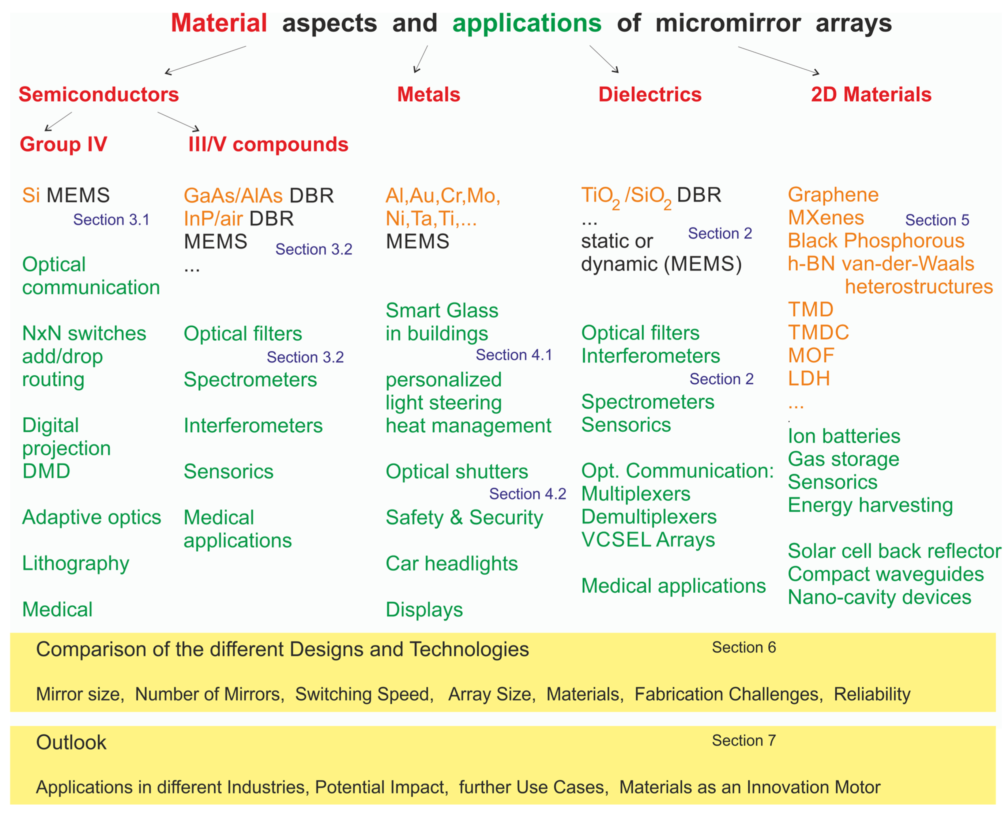
:1. Introduction
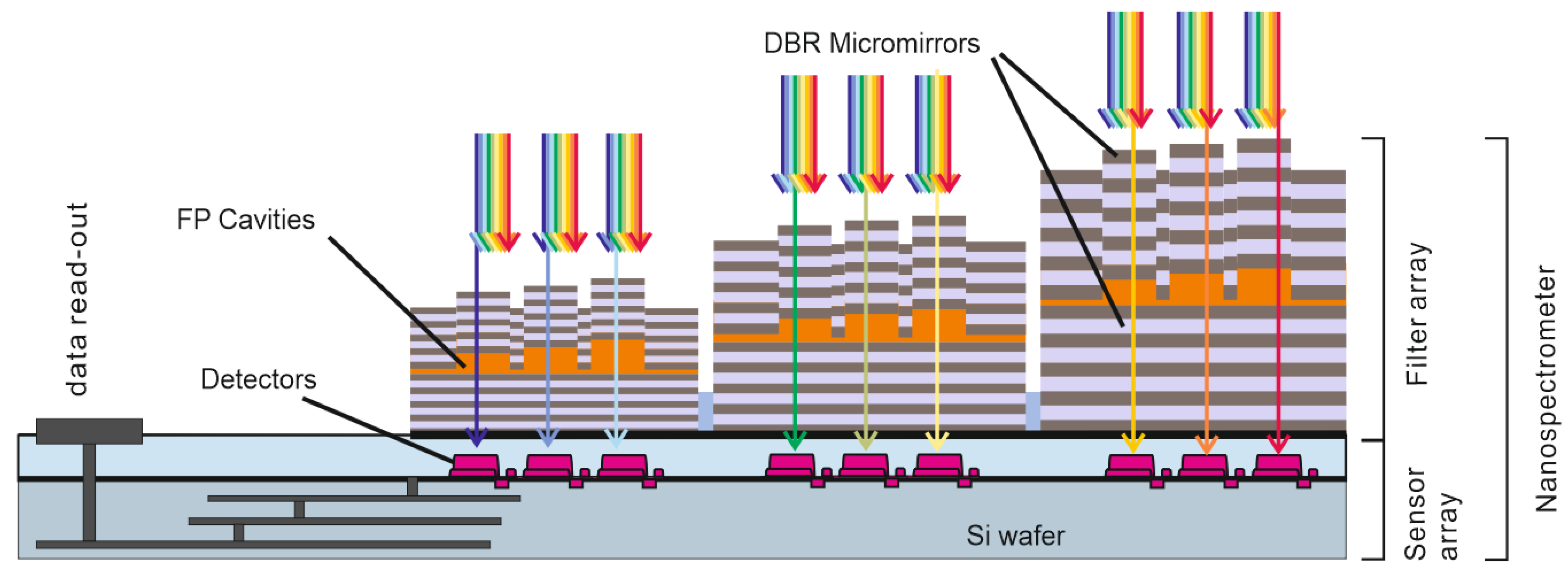
2. Arrays of Dielectric DBR Mirrors
3. Arrays of MEMS Semiconductor Mirrors
3.1. Silicon MEMS Micromirror Arrays
3.2. Compound Semiconductor MEMS Micromirror Arrays
4. Arrays of Metallic MEMS Mirrors for Light-Intensity Modulation and Light Steering
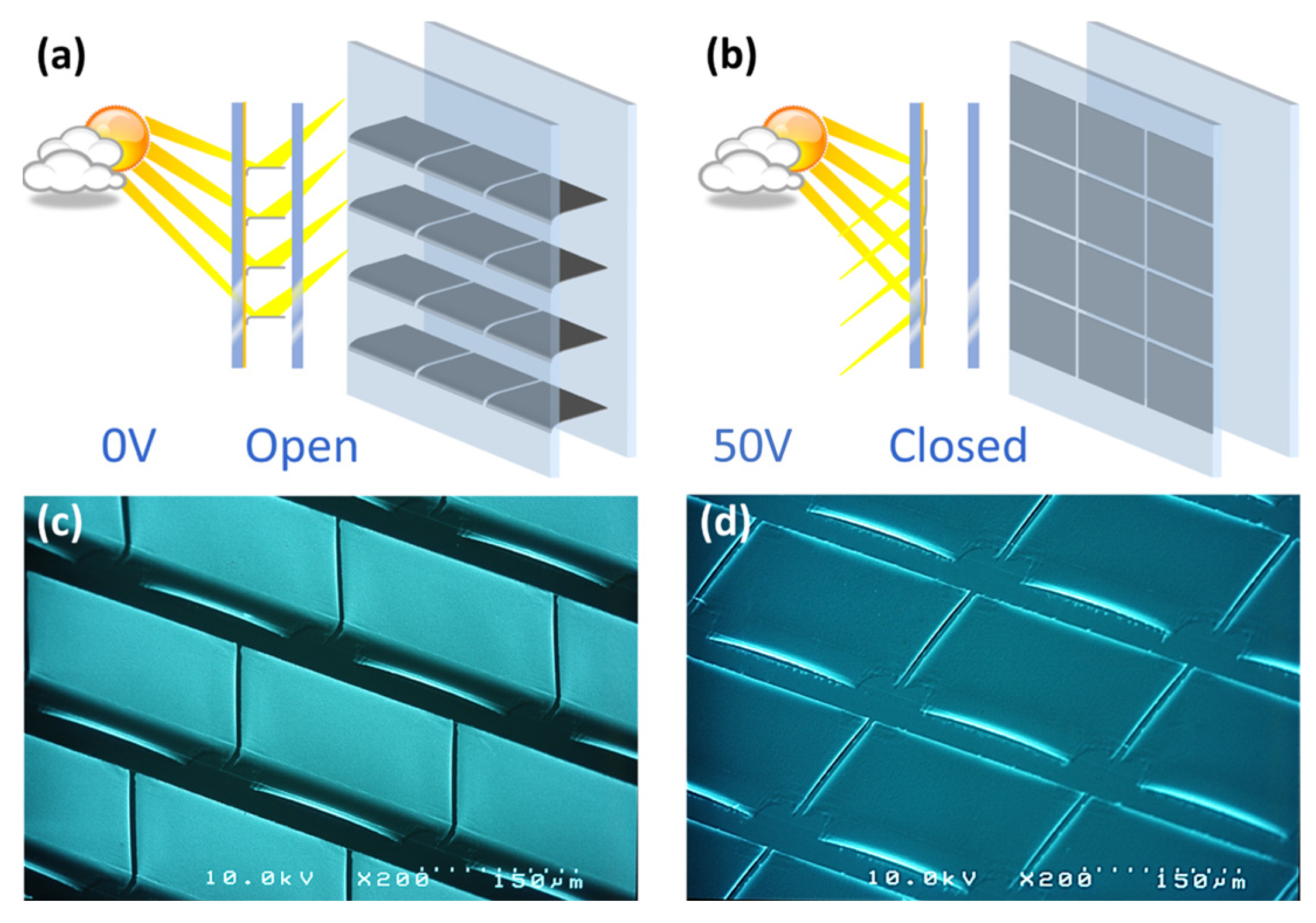
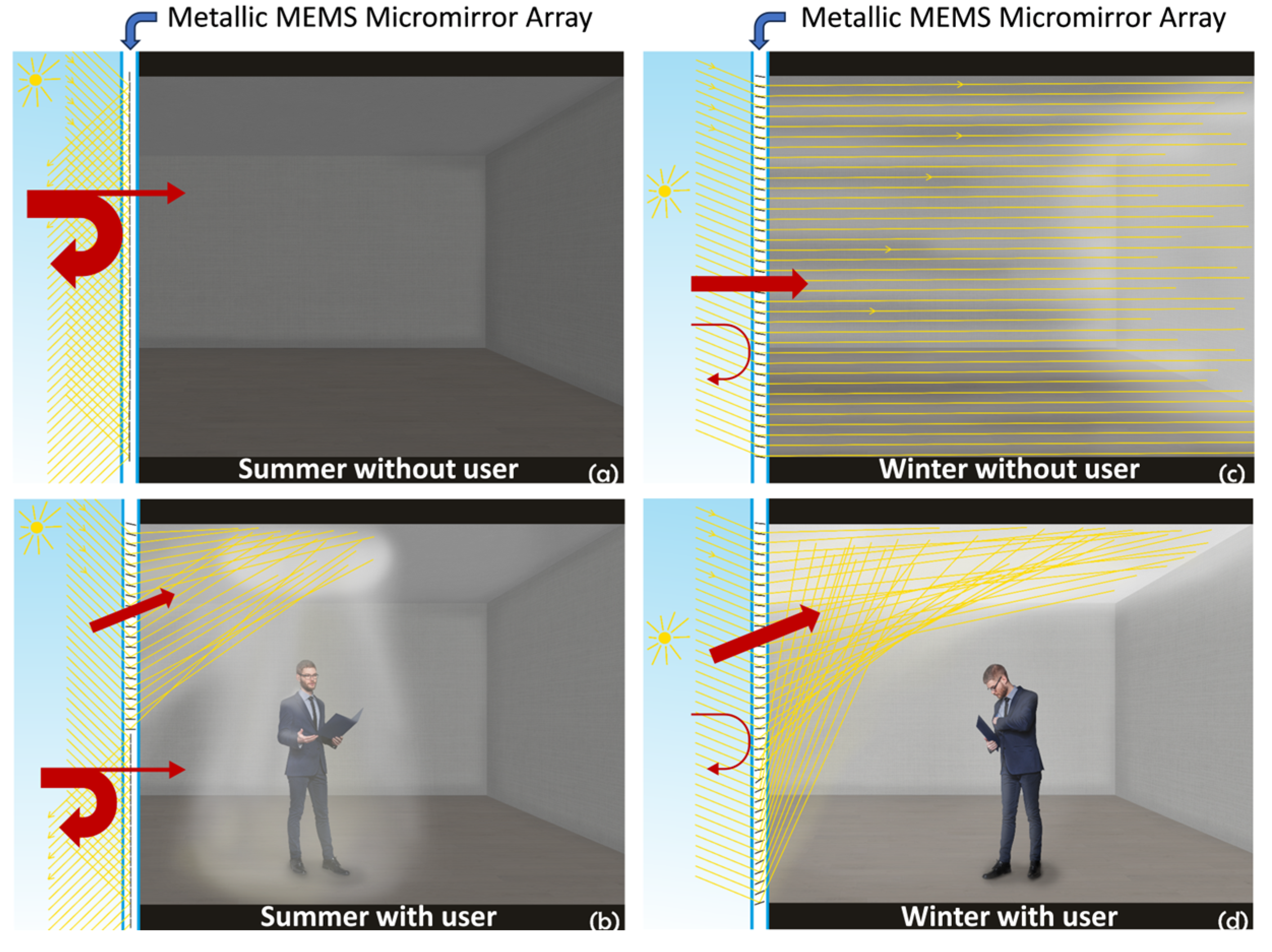
4.1. MEMS Smart Glass for Personalized Light Steering
- Typical electrostatic actuation voltages between 40 V and 60 V were measured. In a single case, an actuation voltage as low as 12 V was measured, and in some cases, 80 V, depending on details in the hinge and the metallic layer stack. Thus, a typical voltage is 50 V.
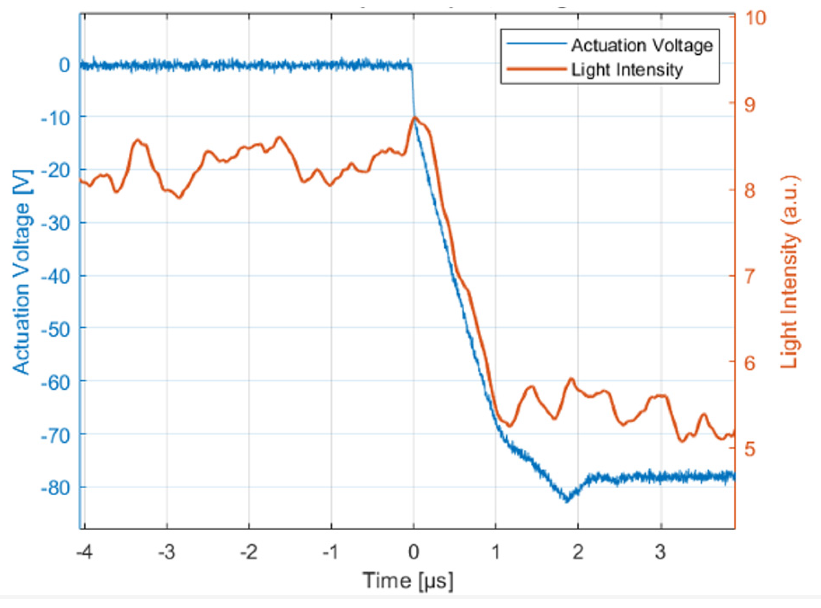
- Switching micromirror arrays from the open to the closed position takes about 0.1 s for arrays with about a sixth of a million mirrors.
- Micromirror arrays were housed in double or quadruple insulation glazing and tested at different temperatures. Between −80 °C and +120 °C, the MEMS micromirrors showed proper actuation. Beyond these extreme temperatures, measurements could not be performed due to the limitations of the used climate chamber.
- The lowest transmission measured in a closed state was 0.01%. The largest transmission measured in an open state was 73%.
- The lowest power consumption in the holding status was 0.2 mW/m2 and < 0.4 mW/m2 during switching.
- Long-term electrostatic actuation at 4 kHz was performed, which corresponds to 38 billion open–closed–open cycles.
- Multiple fast temperature cycles (0 °C to +80 °C to 0 °C to +80 °C to 0 °C to +80 °C and further periodic repetitions) were performed over 225 h without any measurable damage.
- Tests under extreme UV radiation during temperature cycles were performed with double insulation glazing. In these cases, the sun spectrum was emulated by UV LED arrays with many different wavelengths. No changes in the mirror performance were measured after 1600 h of extreme UV exposure, where ten times higher irradiance values were chosen in all spectral parts of the emulated solar UV spectrum than the highest exposure values observed in big global cities.
- Mechanical vibration treatment at 3278 Hz was performed over 31,000 h, without observing mirror damage.
4.2. MEMS Microshutter Arrays for Laser Safety Goggles
4.3. MEMS Ring Shutters for Interference Microscopy (and Endoscopy)
5. The Potential of 2D Materials for Photonic Applications

6. Comparison of the Different Designs and Technologies
6.1. Dimensions, Complexity, Speed, Miniaturization, and Reliability
6.2. Hinges of Micromirrors: Geometry, Methodology, and Fabrication Challenges
- In the DBR micromirror arrays in the example chosen above, the FP-based nanospectrometer includes no hinges since they are static.If very high reflectivity >99.5% is required, the number of periods must be larger than 14.5, and the optical absorption inside the two dielectric layers must be <20 cm−1, which is a challenge. If the SiO2/Si3N4 DBRs and a reflectivity of 99.9% are required, a low absorption of even 10 cm−1 has to be achieved, which is an extreme challenge for deposition machines. The minimum required number of periods is 15.5 for that. In such a case, it would be better to use a dielectric material system with much higher refractive index contrast such as SiO2/ZrO2 or SiO2/TiO2. For more details, see the Supplementary Materials (Figure S1).The potential minimum space requirement for a spectrometer with static dielectric DBR micromirrors might be 0.07 mm2. This is estimated for a wavelength range λ = 400–800 nm and a single micromirror pixel size of 10 × 10 μm2 and TiO2/SiO2 dielectric stacks.The fabrication challenges lay in the requirements for the multilayer deposition to keep the grating period as well as the composition highly constant throughout the whole DBR stack. This requires precision engineering. Using the nanoimprint over several DBR mirror stacks (to combine spectrally different stopbands) [6], this technology is scalable.
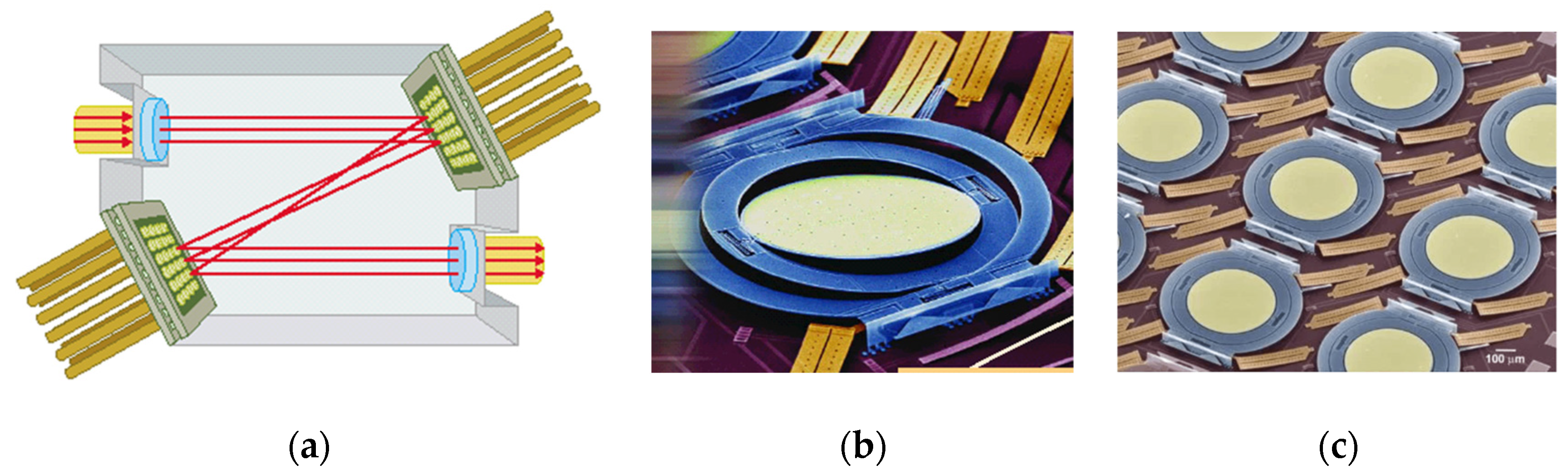
- The hinges of the N2 micromirrors used in the fiber-optic N×N switches are the only ones that are built like a classical door or window hinge, with a pin, a cylindrical airgap, and a surrounding cylindrical barrel. The fabrication requires three sub-steps, amorphous silicon is used for all remaining parts, and SiO2 is used as the sacrificial layer material. The technological process is displayed in Figure 5e. The fabrication process is similar to that described in refs. [3,4,5,89]. One of the challenges is to reduce friction inside the hinge and to overcome the problems of diverging light beams. In addition, it should be noted that this technology does not allowall arbitrary combinations of simultaneous switching processes from input to output.
- The gimbal mount of the 2N micromirrors of the λ-router uses four cantilevers as torsion blades for each mirror. The challenge is to implement the required angle accuracies. Precision engineering is required here.
- Each micromirror of a DMD array uses two cantilevers as torsion blades and two landing tips to stylize a distinct orientation and position. In the projection or dump mode, each mirror plane is defined precisely by three points.One of the multiple challenges that the engineers had to solve was filling the square central hole existing at the beginning.
- The InP multiple airgap micromirrors use four, three, or two cantilevers for each membrane. One end of each cantilever is connected to a solid supporting post, and the other end is deflected vertically to the substrate plane. Four suspensions show the largest stability, three suspensions show the best compromise between stability and wider tunability, and two suspensions reveal the widest tunability but are unstable and can undergo unwanted tilt.
- 6.
- The metallic MEMS micromirror in arrays for smart glass applications in building facades or windows uses blades as hinges that are rolled up and unrolled. The mirror part is planarized and can be tilted in the desired angles via electrostatic actuation. Here, the challenges are to control material stress in the metallic sublayer stress to enable precise hinge bending angles and to allow planarization. In addition, upscaling is challenging.
- 7.
- The metallic MEMS microshutter in arrays for safety goggles uses blades as hinges that are rolled up and unrolled. The shutter part is planarized and actuated electrostatically. Here, to obtain different hinge orientations and high area filling at the same time with no interference and planarity is very challenging.
- 8.
- The metallic MEMS micromirrors for ring shutters in interference microscopes and endoscopes use blades as hinges that are rolled up and unrolled. The mirror part for the ring shutter is planarized and can be tilted in the desired angles via electrostatic actuation.
7. Outlook
8. Conclusions
Supplementary Materials
Author Contributions
Funding
Institutional Review Board Statement
Informed Consent Statement
Data Availability Statement
Acknowledgments
Conflicts of Interest
References
- Solgaard, O.; Godil, A.A.; Howe, R.T.; Lee, L.P.; Peter, Y.-A.; Zappe, H. Optical MEMS: From Micromirrors to Complex Systems. J. Microelectromech. Syst. 2014, 23, 517–538. [Google Scholar] [CrossRef]
- Ren, Y.-X.; Lu, R.-D.; Gong, L. Tailoring light with a digital micromirror device. Ann. Phys. 2015, 527, 447–470. [Google Scholar] [CrossRef]
- Wu, M.C.; Lin, L.-Y.; Lee, S.-S.; Pister, K. Micromachined free-space integrated micro-optics. Sens. Actuators A Phys. 1995, 50, 127–134. [Google Scholar] [CrossRef]
- Wu, M.C. Micromachining for optical and optoelectronic systems. Proc. IEEE 1997, 85, 1833–1856. [Google Scholar] [CrossRef]
- Wu, M.C.; Lin, L.-Y.; Lee, S.-S. Micromachined free space integrated optics. Proc. SPIE 1994, 40–51. [Google Scholar] [CrossRef]
- Hillmer, H.; Woidt, C.; Istock, A.; Kobylinskiy, A.; Nguyen, D.T.; Ahmed, N.; Brunner, R.; Kusserow, T. Role of Nanoimprint Lithography for Strongly Miniaturized Optical Spectrometers. Nanomaterials 2021, 11, 164. [Google Scholar] [CrossRef]
- Correia, J.H.; Bartek, M.; Wolffenbuttel, R.F. High-selectivity single-chip spectrometer in silicon for operation in visible part of the spectrum. IEEE Trans. Electron Devices 2000, 47, 553–559. [Google Scholar] [CrossRef]
- Correia, J.H.; de Graaf, G.; Kong, S.H.; Bartek, M.; Wolffenbuttel, R.F. Single-chip CMOS optical microspectrometer. Sens. Actuators A Phys. 2000, 82, 191–197. [Google Scholar] [CrossRef]
- Wolffenbuttel, R.F. MEMS-based optical mini- and microspectrometers for the visible and infrared spectral range. J. Micromech. Microeng. 2005, 15, S145. [Google Scholar] [CrossRef]
- Wang, S.-W.; Li, M.; Xia, C.-S.; Wang, H.-Q.; Chen, X.-S.; Lu, W. 128 channels of integrated filter array rapidly fabricated by using the combinatorial deposition technique. Appl. Phys. B 2007, 88, 281–284. [Google Scholar] [CrossRef]
- Peerlings, J.; Dehe, A.; Vogt, A.; Tilsch, M.; Hebeler, C.; Langenhan, F.; Meissner, P.; Hartnagel, H.L. Long resonator micromachined tunable GaAs-AlAs Fabry-Perot filter. IEEE Photonics Technol. Lett. 1997, 9, 1235–1237. [Google Scholar] [CrossRef]
- Chitica, N.; Daleiden, J.; Strassner, M.; Streubel, K. Monolithic InP-biased tunable filter with 10-nm bandwidth for optical data interconnects in the 1550-nm band. IEEE Photonics Technol. Lett. 1999, 11, 584–586. [Google Scholar] [CrossRef]
- Tayebati, P.; Wang, P.D.; Vakhshoori, D.; Sacks, R.N. Widely tunable Fabry-Perot filter using Ga(Al)As-AlOx deformable mirrors. IEEE Photonics Technol. Lett. 1998, 10, 394–396. [Google Scholar] [CrossRef]
- Kanbara, N.; Suzuki, K.; Watanabe, T.; Iwaoka, H. Precisely tunable Fabry-Perot filter for optical communications. In Proceedings of the IEEE/LEOS International Conference on Optical MEMs, Lugano, Switzerland, 20–23 August 2002; pp. 173–174. [Google Scholar]
- Tarraf, A.; Daleiden, J.; Irmer, S.; Prasai, D.; Hillmer, H. Stress investigation of PECVD dielectric layers for advanced optical MEMS. J. Micromech. Microeng. 2003, 14, 317. [Google Scholar] [CrossRef]
- Pu, C.; Lin, L.Y.; Goldstein, E.L.; Tkach, R.W. Client-configurable eight-channel optical add/drop multiplexer using micromachining technology. IEEE Photonics Technol. Lett. 2000, 12, 1665–1667. [Google Scholar] [CrossRef]
- Lin, L.Y.; Goldstein, E.L. Opportunities and challenges for MEMS in lightwave communications. IEEE J. Sel. Top. Quantum Electron. 2002, 8, 163–172. [Google Scholar] [CrossRef]
- Aksyuk, V.A.; Pardo, F.; Carr, D.; Greywall, D.; Chan, H.B.; Simon, M.E.; Gasparyan, A.; Shea, H.; Lifton, V.; Bolle, C.; et al. Beam-steering micromirrors for large optical cross-connects. J. Light. Technol. 2003, 21, 634–642. [Google Scholar] [CrossRef]
- Bishop, D.J.; Giles, C.R.; Austin, G.P. The Lucent LambdaRouter: MEMS technology of the future here today. IEEE Commun. Mag. 2002, 40, 75–79. [Google Scholar] [CrossRef]
- Duncan, W.M.; Bartlett, T.; Lee, B.; Powell, D.; Rancuret, P.; Sawyers, B. Dynamic optical filtering in DWDM systems using the DMD. Solid-State Electron. 2002, 46, 1583–1585. [Google Scholar] [CrossRef]
- Ballard, B.; Bhakta, V.; Douglass, M.; Gelabert, P.; Kempf, J.; McDonald, W.; Pettitt, G.; Rancuret, P.; Rankin, A.; Thompson, J.; et al. 5-1: Invited Paper: ‘Steering’ Light with Texas Instruments Digital Micromirror Device (DMD)-Past, Present & Future. SID Symp. Dig. Tech. Pap. 2016, 47, 28–31. [Google Scholar] [CrossRef]
- Bifano, T. MEMS deformable mirrors. Nat. Photonics 2011, 5, 21–23. [Google Scholar] [CrossRef]
- Manzanera, S.; Helmbrecht, M.A.; Kempf, C.J.; Roorda, A. MEMS segmented-based adaptive optics scanning laser ophthalmoscope. Biomed. Opt. Express 2011, 2, 1204–1217. [Google Scholar] [CrossRef] [PubMed]
- Zhu, G.; Levine, J.; Praly, L.; Peter, Y.-A. Flatness-Based Control of Electrostatically Actuated MEMS with Application to Adaptive Optics: A Simulation Study. J. Microelectromech. Syst. 2006, 15, 1165–1174. [Google Scholar] [CrossRef]
- Hillmer, H.; Woidt, C.; Kobylinskiy, A.; Kraus, M.; Istock, A.; Iskhandar, M.S.Q.; Brunner, R.; Kusserow, T. Miniaturized Interferometric Sensors with Spectral Tunability for Optical Fiber Technology—A Comparison of Size Requirements, Performance, and New Concepts. Photonics 2021, 8, 332. [Google Scholar] [CrossRef]
- Kusserow, T.; Dharmarasu, N.; Hillmer, H. Materials: Compound semiconductors. In Comprehensive Microsystems, Fundamentals, Technology and Applications; Elsevier: Amsterdam, The Netherlands, 2024; in print. [Google Scholar]
- Hasan, M.K.; Baby, S.; Muringakodan, S.; Nandakumar, A.; Iskhandar, M.S.Q.; Hillmer, V.; Li, Q.; Xu, G.; Hillmer, H. Energy Saving and Amortization Time Simulation for a Model Room with MEMS Smart Glazing; Jahrbuch Oberflächentechnik; Eugen G. Leuze Verlag: Bad Saulgau, Germany, 2022; ISBN 978-3-87480-369-4. [Google Scholar]
- Löber, D.; Kamrul Hasan, M.; Liebermann, S.; Siddi Que Iskhandar, M.; Baby, S.; Chen, J.; Farrag, E.; Ahmed, N.; Liu, S.; Elsaka, B.; et al. MEMS Smart Glass for Personalized Lighting and Energy Management in Buildings: Working Principles, Characterization, Active Light Steering, Thermal Management, Energy Saving Considering Different Locations on Earth, Comparison of Different Smart Glass Technologies. J. Build. Des. Environ. 2023, 2. [Google Scholar] [CrossRef]
- Hillmer, H.; Iskhandar, M.S.Q.; Hasan, M.; Akhundzada, S.; Al-Qargholi, B.; Tatzel, A. MOEMS micromirror arrays in smart windows for daylight steering. J. Opt. Microsyst. 2021, 1, 14502. [Google Scholar] [CrossRef]
- Hillmer, H.; Al-Qargholi, B.; Mohsin Khan, M.; Worapattrakul, N.; Wilke, H.; Woidt, C.; Tatzel, A. Optical MEMS-based micromirror arrays for active light steering in smart windows. Jpn. J. Appl. Phys. 2018, 57, 08PA07. [Google Scholar] [CrossRef]
- Hasan, M.K.; Liebermann, S.; Iskhandar, M.; Löber, D.; Li, Q.; Xu, G.; Hillmer, H. Personalized Light Steering in Buildings Utilizing 2D Actuation in MEMS Micromirror Arrays. In Yearbook Surface Technology; Leuze Publishing House: Bad Saulgau, Germany, 2022; pp. 217–237. ISBN 978-3-87480-380-9. [Google Scholar]
- Iskhandar, M.S.Q.; Al-Qargholi, B.; Khan, M.M.; Tatzel, A.; Luo, H.; Nazemroaya, S.; Li, Q.; Hillmer, H. Development of optical MEMS-based micromirror arrays for smart window applications: Implementation of subfield addressing and reliability measurements. In Yearbook Surface Technology; Leuze Publishing House: Bad Saulgau, Germany, 2019; pp. 93–107. ISBN 978-3-87480-357-1. [Google Scholar]
- Nazemroaya, S.; Iskhandar, M.; Hasan, M.K.; Li, Q.; Hillmer, H. Concepts for clear View through 3D Structured Surfaces of MEMS Smart Glass: Design, Implementation, Characterization and Validation. In Yearbook Surface Technology; Leuze Publishing House: Bad Saulgau, Germany, 2020; pp. 101–115. ISBN 978-3-87480-364-9. [Google Scholar]
- Qasim, H.M.; Chen, J.; Iskhandar, M.; Hasan, M.; Baby, S.; Elsaka, B.; Löber, D.; Xu, G.; Hillmer, H. Advancements in Surface Modification and Coloring Technologies for MEMS-Based Smart Windows: Ultra-Thin Highly Absorbing Films and C-V Measurements of Smart Glass as Sustainable Energy Solutions. In Yearbook Surface Technology; Leuze Publishing House: Bad Saulgau, Germany, 2023; pp. 336–372. ISBN 978-3-87480-385-4. [Google Scholar]
- Ilias, S.; Picard, F.; Larouche, C.; Kruzelecky, R.; Jamroz, W.; Le Noc, L.; Topart, P. Programmable optical microshutter arrays for large aspect ratio microslits. In Photonics North 2008; Vallée, R., Piché, M., Mascher, P., Cheben, P., Côté, D., LaRochelle, S., Schriemer, H.P., Albert, J., Ozaki, T., Eds.; SPIE, Bellingham: Washington, DC, USA, 2008; p. 70992D. [Google Scholar]
- Goodwin-Johansson, S.; Davidson, M.; Dausch, D.; Holloway, P.H.; McGuire, G. High speed, large motion electrostatic artificial eyelid. In Technical Digest, Proceedings of the MEMS 2002 IEEE International Conference, Fifteenth IEEE International Conference on Micro Electro Mechanical Systems (Cat. No.02CH37266); IEEE: Piscataway, NJ, USA, 2002; pp. 610–613. [Google Scholar]
- Kim, C.-H.; Hong, S. Study on the reliability of the mechanical shutter utilizing roll actuators. In Proceedings of the 2011 IEEE 24th International Conference on Micro Electro Mechanical Systems, Cancun, Mexico, 23–27 January 2011; pp. 501–504. [Google Scholar]
- Pizzi, M.; Koniachkine, V.; Nieri, M.; Sinesi, S.; Perlo, P. Electrostatically driven film light modulators for display applications. Microsyst. Technol. 2003, 10, 17–21. [Google Scholar] [CrossRef]
- Roux, P.; Woirgard, E.; Pizzi, M.; de Martiis, O.; Koniachkine, V. Fem modelling of an electro-optical micro-shutter. Sens. Actuators A Phys. 2005, 119, 1–7. [Google Scholar] [CrossRef]
- Schalberger, P.; Al Nusayer, S.A.; Raichle, C. 54-1: Parallel Fabrication for Integration of Electronic and Microelectromechanical Systems. SID Symp. Dig. Technol. Pap. 2016, 47, 731–734. [Google Scholar] [CrossRef]
- Mori, K.; Misawa, K.; Ihida, S.; Takahashi, T.; Fujita, H.; Toshiyoshi, H. A MEMS Electrostatic Roll-Up Window Shade Array for House Energy Management System. IEEE Photonics Technol. Lett. 2016, 28, 593–596. [Google Scholar] [CrossRef]
- Lamontagne, B.; Fong, N.R.; Song, I.-H.; Ma, P.; Barrios, P.J.; Poitras, D. Review of microshutters for switchable glass. J. Micro/Nanolithogr. MEMS MOEMS 2019, 18, 40901. [Google Scholar] [CrossRef]
- Langley, D.; Rogers, S.; Starman, L. Fabrication Studies for Scaling Photonic MEMS Micro-shutter Designs. In Adaptive Coded Aperture Imaging and Non-Imaging Sensors II: 10 August 2008, San Diego, California, USA; Casasent, D.P., Ed.; SPIE: Bellingham, DC, USA, 2008; ISBN 9780819473165. [Google Scholar]
- Goodwin-Johansson, S.H.; Davidson, M.R.; Dausch, D.E.; Holloway, P.H.; McGuire, G. Reduced voltage artificial eyelid for protection of optical sensors. Proc. SPIE 2002, 451–458. [Google Scholar]
- Lamontagne, B.; Barrios, P.; Py, C.; Nikumb, S. The next generation of switchable glass: The micro-blinds. In Proceedings of the Conference Glass Performance Days, Collection/Collection: NRC Publications Archive/Archives des publications du CNRC. June 2009. Available online: https://nrc-publications.canada.ca/eng/view/accepted/?id=6c7d2744-b6af-47fd-9a51-9b5c6a2f48ad (accessed on 26 February 2024).
- Schlam, E.; Finch, J.; Koskulics, J. Highly Reflective Electrostatic Shutter Display; Campbell; Society for Information Display: Sendai, Japan, 2017. [Google Scholar]
- Kim, C.-H.; Jung, K.-D.; Kim, W. A Wafer-Level Micro Mechanical Global Shutter for a Micro Camera. In Proceedings of the 2009 IEEE 22nd International Conference on Micro Electro Mechanical Systems, Sorrento, Italy, 25–29 January 2009; pp. 156–159. [Google Scholar]
- Lee, K.-H.; Chang, J.; Yoon, J.-B. High performance microshutter device with space-division modulation. J. Micromech. Microeng. 2010, 20, 75030. [Google Scholar] [CrossRef]
- Lim, K.-S.; Chung, J.; Yoo, S.; Yoon, J.-B. P-67: Wide Bandwidth Reflective Microshutter Blind Panel for Transparent Organic Light-Emitting Diode Display. SID Symp. Dig. Tech. Pap. 2016, 47, 1389–1391. [Google Scholar] [CrossRef]
- Al Nusayer, S.A.; Schalberger, P.; Baur, H.; Fruehauf, N. 39-4: TFT Integrated Microelectromechanical Shutter for Display Application. SID Symp. Dig. Tech. Pap. 2018, 49, 498–501. [Google Scholar] [CrossRef]
- Yang, X.; Kästner, P.; Käkel, E.; Smolarczyk, M.; Liu, S.; Li, Q.; Hillmer, H. Study of Dynamics in Metallic MEMS Cantilevers—Pull-In Voltage and Actuation Speed. Appl. Sci. 2023, 13, 1118. [Google Scholar] [CrossRef]
- Künne, M.; Hagemeier, S.; Käkel, E.; Hillmer, H.; Lehmann, P. Investigation of measurement data of low-coherence interferometry at tilted surfaces in the 3D spatial frequency domain. tm-Technol. Mess. 2022, 89, 515–524. [Google Scholar] [CrossRef]
- Zhou, G.; Yu, H.; Du, Y.; Chau, F.S. Microelectromechanical-systems-driven two-layer rotary-blade-based adjustable iris diaphragm. Opt. Lett. 2012, 37, 1745–1747. [Google Scholar] [CrossRef]
- Draheim, J.; Burger, T.; Korvink, J.G.; Wallrabe, U. Variable aperture stop based on the design of a single chamber silicone membrane lens with integrated actuation. Opt. Lett. 2011, 36, 2032–2034. [Google Scholar] [CrossRef]
- Muller, P.; Feuerstein, R.; Zappe, H. Integrated Optofluidic Iris. J. Microelectromech. Syst. 2012, 21, 1156–1164. [Google Scholar] [CrossRef]
- Deutschmann, T.; Oesterschulze, E. Integrated electrochromic iris device for low power and space-limited applications. J. Opt. 2014, 16, 75301. [Google Scholar] [CrossRef]
- Schuhladen, S.; Preller, F.; Rix, R.; Petsch, S.; Zentel, R.; Zappe, H. Iris-Like Tunable Aperture Employing Liquid-Crystal Elastomers. Adv. Mater. 2014, 26, 7247–7251. [Google Scholar] [CrossRef]
- Zeng, H.; Wani, O.M.; Wasylczyk, P.; Kaczmarek, R.; Priimagi, A. Self-Regulating Iris Based on Light-Actuated Liquid Crystal Elastomer. Adv. Mater. 2017, 29, 1701814. [Google Scholar] [CrossRef]
- Ma, Q.; Ren, G.; Xu, K.; Ou, J.Z. Tunable Optical Properties of 2D Materials and Their Applications. Adv. Opt. Mater. 2021, 9, 2001313. [Google Scholar] [CrossRef]
- Kim, H.-L.; Wang, F. Reflective Phase-Contrast for High-Contrast Imaging of van der Waals Heterostructure. Nano Lett. 2023, 23, 2898–2904. [Google Scholar] [CrossRef]
- Ye, K.; Liu, L.; Huang, J.; Nie, A.; Zhai, K.; Wang, B.; Wen, F.; Mu, C.; Zhao, Z.; Gong, Y.; et al. High-Performance Broadband Photodetectors of Heterogeneous 2D Inorganic Molecular Sb2O3/Monolayer MoS2 Crystals Grown via Chemical Vapor Deposition. Adv. Opt. Mater. 2020, 8, 2000168. [Google Scholar] [CrossRef]
- Carvalho, A.F.; Kulyk, B.; Fernandes, A.J.S.; Fortunato, E.; Costa, F.M. A Review on the Applications of Graphene in Mechanical Transduction. Adv. Mater. 2022, 34, 2101326. [Google Scholar] [CrossRef]
- Kim, S. All-2D material photonic devices. Nanoscale Adv. 2023, 5, 323–328. [Google Scholar] [CrossRef]
- Koppens, F.H.L.; Mueller, T.; Avouris, P.; Ferrari, A.C.; Vitiello, M.S.; Polini, M. Photodetectors based on graphene, other two-dimensional materials and hybrid systems. Nat. Nanotechnol. 2014, 9, 780–793. [Google Scholar] [CrossRef] [PubMed]
- Jeon, J.; Yang, Y.; Choi, H.; Park, J.-H.; Lee, B.H.; Lee, S. MXenes for future nanophotonic device applications. Nanophotonics 2020, 9, 1831–1853. [Google Scholar] [CrossRef]
- Yu, L.; Bati, A.S.R.; Grace, T.S.L.; Batmunkh, M.; Shapter, J.G. Ti3C2Tx (MXene)-Silicon Heterojunction for Efficient Photovoltaic Cells. Adv. Energy Mater. 2019, 9, 1901063. [Google Scholar] [CrossRef]
- Zheng, W.; Jiang, Y.; Hu, X.; Li, H.; Zeng, Z.; Wang, X.; Pan, A. Light Emission Properties of 2D Transition Metal Dichalcogenides: Fundamentals and Applications. Adv. Opt. Mater. 2018, 6, 1800420. [Google Scholar] [CrossRef]
- Anichini, C.; Czepa, W.; Pakulski, D.; Aliprandi, A.; Ciesielski, A.; Samorì, P. Chemical sensing with 2D materials. Chem. Soc. Rev. 2018, 47, 4860–4908. [Google Scholar] [CrossRef] [PubMed]
- Geim, A.K.; Grigorieva, I.V. Van der Waals heterostructures. Nature 2013, 499, 419–425. [Google Scholar] [CrossRef] [PubMed]
- Castellanos-Gomez, A.; Duan, X.; Fei, Z.; Gutierrez, H.R.; Huang, Y.; Huang, X.; Quereda, J.; Qian, Q.; Sutter, E.; Sutter, P. Van der Waals heterostructures. Nat. Rev. Methods Primers 2022, 2, 1–19. [Google Scholar] [CrossRef]
- Papadakis, G.T.; Narang, P.; Sundararaman, R.; Rivera, N.; Buljan, H.; Engheta, N.; Soljačić, M. Ultralight Angstrom-Scale Optimal Optical Reflectors. ACS Photonics 2018, 5, 384–389. [Google Scholar] [CrossRef]
- Mak, K.F.; Shan, J. Photonics and optoelectronics of 2D semiconductor transition metal dichalcogenides. Nat. Photonics 2016, 10, 216–226. [Google Scholar] [CrossRef]
- Li, Q.; Alfrey, A.; Hu, J.; Lydick, N.; Paik, E.; Liu, B.; Sun, H.; Lu, Y.; Wang, R.; Forrest, S.; et al. Macroscopic transition metal dichalcogenides monolayers with uniformly high optical quality. Nat. Commun. 2023, 14, 1837. [Google Scholar] [CrossRef]
- Zeytinoǧlu, S.; Roth, C.; Huber, S.; İmamoğlu, A. Atomically thin semiconductors as nonlinear mirrors. Phys. Rev. A 2017, 96, 31801. [Google Scholar] [CrossRef]
- van de Groep, J.; Song, J.-H.; Celano, U.; Li, Q.; Kik, P.G.; Brongersma, M.L. Exciton resonance tuning of an atomically thin lens. Nat. Photonics 2020, 14, 426–430. [Google Scholar] [CrossRef]
- Ma, E.Y.; Hu, J.; Waldecker, L.; Watanabe, K.; Taniguchi, T.; Liu, F.; Heinz, T.F. The Reststrahlen Effect in the Optically Thin Limit: A Framework for Resonant Response in Thin Media. Nano Lett. 2022, 22, 8389–8393. [Google Scholar] [CrossRef] [PubMed]
- Back, P.; Zeytinoglu, S.; Ijaz, A.; Kroner, M.; Imamoğlu, A. Realization of an Electrically Tunable Narrow-Bandwidth Atomically Thin Mirror Using Monolayer MoSe2. Phys. Rev. Lett. 2018, 120, 37401. [Google Scholar] [CrossRef] [PubMed]
- Suárez-Forero, D.G.; Ni, R.; Sarkar, S.; Mehrabad, M.J.; Mechtel, E.; Simonyan, V.; Grankin, A.; Watanabe, K.; Taniguchi, T.; Park, S.; et al. Chiral Optical Nano-Cavity with Atomically Thin Mirrors. arXiv 2023, arXiv:2308.04574. [Google Scholar]
- Rui, J.; Wei, D.; Rubio-Abadal, A.; Hollerith, S.; Zeiher, J.; Stamper-Kurn, D.M.; Gross, C.; Bloch, I. A subradiant optical mirror formed by a single structured atomic layer. Nature 2020, 583, 369–374. [Google Scholar] [CrossRef]
- Lin, L.Y.; Goldstein, E.L.; Tkach, R.W. Free-space micromachined optical switches for optical networking. IEEE J. Sel. Top. Quantum Electron. 1999, 5, 4–9. [Google Scholar] [CrossRef]
- Lin, L.Y.; Goldstein, E.L. Micro-electro-mechanical systems (MEMS) for WDM optical-crossconnect networks. In Proceedings of the MILCOM 1999, IEEE Military Communications, Conference Proceedings (Cat. No. 99CH36341), Atlantic City, NJ, USA, 31 October–3 November 1999; Volume 2, pp. 954–957. [Google Scholar]
- Texas Instruments. Incorporated [DLPS036; B]. DLP9000 Family of 0.9 WQXGA Type A DMDs datasheet (Rev. B). Available online: https://www.ti.com/lit/ds/symlink/dlp9000.pdf?ts=1706718124684&ref_url=https%253A%252F%252Fwww.ti.com%252Fsitesearch%252Fen-us%252Fdocs%252Funiversalsearch.tsp%253FlangPref%253Den-US%2526searchTerm%253DDLP9000%2526nr%253D310 (accessed on 23 February 2024).
- Texas Instruments. Incorporated [DLPS221; B]. DLP780TE 0.78 4K UHD DMD datasheet (Rev. B). Available online: https://www.ti.com/lit/ds/symlink/dlp780te.pdf?ts=1706518601346 (accessed on 23 February 2024).
- Texas Instruments. Incorporated [DLPA083; B]. DMD Optical Efficiency for Visible Wavelengths (Rev. B). Available online: https://www.ti.com/lit/an/dlpa083b/dlpa083b.pdf?ts=1706539387115&ref_url=https%253A%252F%252Fwww.ti.com%252Fsitesearch%252Fen-us%252Fdocs%252Funiversalsearch.tsp%253FlangPref%253Den-US%2526searchTerm%253Ddmd%2B13%2B68%2526nr%253D195 (accessed on 23 February 2024).
- Texas Instruments. Incorporated [DLPS033; D]. DLP9500UV DLP® 0.95 UV 1080p 2 x LVDS Type A DMD datasheet (Rev. D). Available online: https://www.ti.com/lit/ds/symlink/dlp9500uv.pdf?ts=1706499386582 (accessed on 26 February 2024).
- Texas Instruments. Incorporated [DLPS061; E]. DLP7000UV 0.7XGA 2xLVDS UV Type A DMD datasheet (Rev. E). Available online: https://www.ti.com/lit/ds/symlink/dlp7000uv.pdf?ts=1706539591407&ref_url=https%253A%252F%252Fwww.ti.com%252Fsitesearch%252Fen-us%252Fdocs%252Funiversalsearch.tsp%253FlangPref%253Den-US%2526searchTerm%253Ddmd%2B13%2B68%2526nr%253D195 (accessed on 23 February 2024).
- Texas Instruments. Incorporated [DLPS125; C]. DLP47100.47 1080p DMD datasheet (Rev. C). Available online: https://www.ti.com/lit/ds/symlink/dlp4710.pdf?ts=1706525566533 (accessed on 23 February 2024).
- Lee, S.-S.; Huang, L.-S.; Kim, C.-J.; Wu, M.C. Free-space fiber-optic switches based on MEMS vertical torsion mirrors. J. Light. Technol. 1999, 17, 7–13. [Google Scholar] [CrossRef]
- Piyawattanametha, W.; Patterson, P.; Wu, M.; Hah, D.; Toshiyoshi, H. A surface and bulk micromachined angular vertical combdrive for scanning micromirrors. In Proceedings of the OFC 2003 Optical Fiber Communications Conference, Atlanta, GA, USA, 28 March 2003; Volume 1, pp. 251–252. [Google Scholar]
- Tan, T.; Jiang, X.; Wang, C.; Yao, B.; Zhang, H. 2D Material Optoelectronics for Information Functional Device Applications: Status and Challenges. Adv. Sci. 2020, 7, 2000058. [Google Scholar] [CrossRef]
- Nanoscale. Available online: https://www.nanoscale-glasstec.de/ (accessed on 23 February 2024).


| Research Group | Time Period | Bottom Electrode | Top Electrode | Mirror Size | Actuation | Speed To Close | Array Size | Max/Min Transmission %–Contrast | Applications, Comments |
|---|---|---|---|---|---|---|---|---|---|
| Fiat [35,36] | 1999–2005 | ITO | flexible metal layer | 458 µm–2.4 mm | 20–100 V | 0.1 ms | - | 20/1–20 | Micro-shutter-based automotive display, IR spectrometry, low transmission |
| MCNC [44] | 2000–2002 | ITO | polyimide/Cr/Au/ polyimide | <100 µm to >200 µm | 100–300 V | 18 µs | 5 cm2 | low contrast | eyelid for protection |
| Kassel University [27,28,29,30,31,32,33,34] | 2003–present | FTO, ITO, or Ag low-e | SiO2-SiNx/Al-Cr-Al/Al-Cr-Al-Ge | 150 × 400 µm2 | 12–80 V | 0.1 s | 0.87 m2 | 73/0.01–7300 high contrast | sunlight steering for buildings, high contrast, low voltage |
| Kassel University [32,33] | 2018–present | FTO, ITO | Al-Cr-Al/Al-Cr-Al | 60 × 1000 µm2 100 × 1000 µm2 | 50–80 V | 1 µs | 7 cm2 | 77/0.01–7700 high contrast | Laser safety goggles, high contrast, high closing speed |
| NRC [42,45] | 2005–present | SnO2, ITO, Ag low-e | Cr and others | 50–300 µm2 | 15–25 V | 40 µs | 20 cm2 | 60/0.1–600 high contrast | high contrast, low voltage |
| NVMG [36,46] | 2007–present | TCO | Shrinkable Polymer | ≥2 mm | 100–500 V | Seconds | 5000 cm2 | low contrast | Macro-curling shutter, commercialized |
| INO [39,42] | 2008–2009 | Al | MoCr | 60 × 1000 µm2 | 110 V | 2 ms to close, 7 ms to open | 0.25 cm2 | low contrast | Space instrumentation |
| Air Force [43] | 2008 | AlZnO | Ti and Au | 200 × 50 µm2 | - | - | - | 40/1–40 | Adaptive coded aperture imaging |
| Samsung [37,47] | 2009–2011 | ITO | Al-SiNx, Mo-Mo | ᴓ 2.2 mm, 36 × 1.4 mm long triangals rolled | 30 V | 2 ms | Iris of 0.04 cm2 | ? | Iris shutter for camera |
| KAIST [48,49] | 2010–2016 | ITO | Electroplated Ni | 200 × 160 µm2 | 20-30 V | 20 µs to close | small | 60/ ?–? | active transparent display with TR-OLEDs |
| University of Tokyo [41] | 2015–2016 | ITO | Al-SiO2 | 200 × 30 µm2 | 38–55 V | 3 ms | - | 53/36–1.5 | implemented on TFT |
| Stuttgart University [42,50] | 2016–present | MoTa | MoTa on stressed SiNx | 200 µm | 20–60 V | - | 2–225 cm2 | low contrast | Transmissive display on TFT, low transmission |
| No. | Materials and Type of Arrays | Number of Micromirrors | Array Size | Dimensions of A Single Mirror | Reflectivity %, Wavelength Range In nm | Switching Time | Miniaturization Potential of a Single Mirror | Reliability, Lifetimes |
|---|---|---|---|---|---|---|---|---|
| 1 | Dielectric DBRs [6] | 384 mirrors | 90 mm2 | 40 µm × 40 µm | 99.8 for 400–1700 nm *** | - | 6 µm × 6 µm for VIS | high, very long for static DBRs |
| 13 µm × 13 µm for NIR | ||||||||
| 2 | Si micromirrors with gold, dielectric coating, N × N switch [80,81] | 64 (8 × 8) | 100 mm2 | Ø = 400 µm | 500 µs mirror itself | |||
| 36 (6 × 6) | ||||||||
| 560 µs with springs | ||||||||
| 3 | Si micromirrors λ-router [16,19] | 256 (16 × 16) | 2.5 cm2 | Ø = 500 µm | <5 ms | 18 billion actuation cycles, long | ||
| 1296 (36 × 36) | ≈36 cm2 | |||||||
| 4 | Si micromirrors DMD [82,83,84,85,86,87] * | 1024 × 768 | ≈14 × 10.5 mm2 | 13.68 µm | 89 for 420−680 nm 88 for 363−420 nm | 12.5 µs | >500 million actuation cycles per mirror, >20 years ** | |
| 1920 × 1080 | ≈20.7 × 11.7 mm2 | 10.8 µm | 12.5 µs | |||||
| 2560 × 1600 | ≈19.4 × 12. mm2 | 7.56 µm (± 12°) | 16 µs | |||||
| 3840 × 2160 | ≈17.3 × 9.7 mm2 | 9 µm (± 14.5°) | 8 µs | |||||
| 1920 × 1080 | ≈ 10.4 × 5.8 mm2 | 5.4 µm (±17°) | 10 µs | |||||
| 5 | InP multiple airgap micromirrors [26] | 306 | 70 mm2 | Various Ø=10 µm–80 µm | 99.995 for a DBR micromirror with 4.5 InP/air periods *** | Simulated <10 µs | Membrane Ø = 13 µm for λ = 1.55 µm | |
| 6 | Metal micromirror arrays for smart glass [27,28,29,30,31,32,33,34] | >1,200,000 | 29 × 29 cm2 | 400 µm × 150 µm | ≈90 at 600 nm | ≈0.1 s | not recommended for smart glass in buildings | 31,000 h vibration tests, 37 billion actuation cycles |
| >12,600,000 | 126 × 69 cm2 | |||||||
| 7 | Metal microshutter arrays for safety goggles [32,33] | up to 10,000 | elliptical main axis 3 cm and 2.5 cm | 1000 µm × 100 µm and many other dimensions | ≈90 at 600 nm | 1 µs | 20 µm | |
| 8 | Metal microshutter arrays for ring shutters | 3000–10,000 | Ø = 18 mm | Lφ = 150–600 µm Lr = 60–300 µm (various dimensions) | ≈ 90 at 600 nm | ≈10 µs interpolated | not required for interference microscopy |
Disclaimer/Publisher’s Note: The statements, opinions and data contained in all publications are solely those of the individual author(s) and contributor(s) and not of MDPI and/or the editor(s). MDPI and/or the editor(s) disclaim responsibility for any injury to people or property resulting from any ideas, methods, instructions or products referred to in the content. |
© 2024 by the authors. Licensee MDPI, Basel, Switzerland. This article is an open access article distributed under the terms and conditions of the Creative Commons Attribution (CC BY) license (https://creativecommons.org/licenses/by/4.0/).
Share and Cite
Liu, S.; Kästner, P.; Donatiello, R.; Shrivastava, A.; Smolarczyk, M.; Iskhandar, M.S.Q.; Hasan, M.K.; Caruso, G.; Chen, J.; Elsaka, B.; et al. State-of-the-Art Materials Used in MEMS Micromirror Arrays for Photonic Applications. Photonics 2024, 11, 253. https://doi.org/10.3390/photonics11030253
Liu S, Kästner P, Donatiello R, Shrivastava A, Smolarczyk M, Iskhandar MSQ, Hasan MK, Caruso G, Chen J, Elsaka B, et al. State-of-the-Art Materials Used in MEMS Micromirror Arrays for Photonic Applications. Photonics. 2024; 11(3):253. https://doi.org/10.3390/photonics11030253
Chicago/Turabian StyleLiu, Shujie, Philipp Kästner, Roland Donatiello, Anup Shrivastava, Marek Smolarczyk, Mustaqim Siddi Que Iskhandar, Md Kamrul Hasan, Giuseppe Caruso, Jiahao Chen, Basma Elsaka, and et al. 2024. "State-of-the-Art Materials Used in MEMS Micromirror Arrays for Photonic Applications" Photonics 11, no. 3: 253. https://doi.org/10.3390/photonics11030253