Integrated Encapsulation and Implementation of a Linear-Mode APD Detector for Single-Pixel Imaging Lidar

Abstract
:1. Introduction
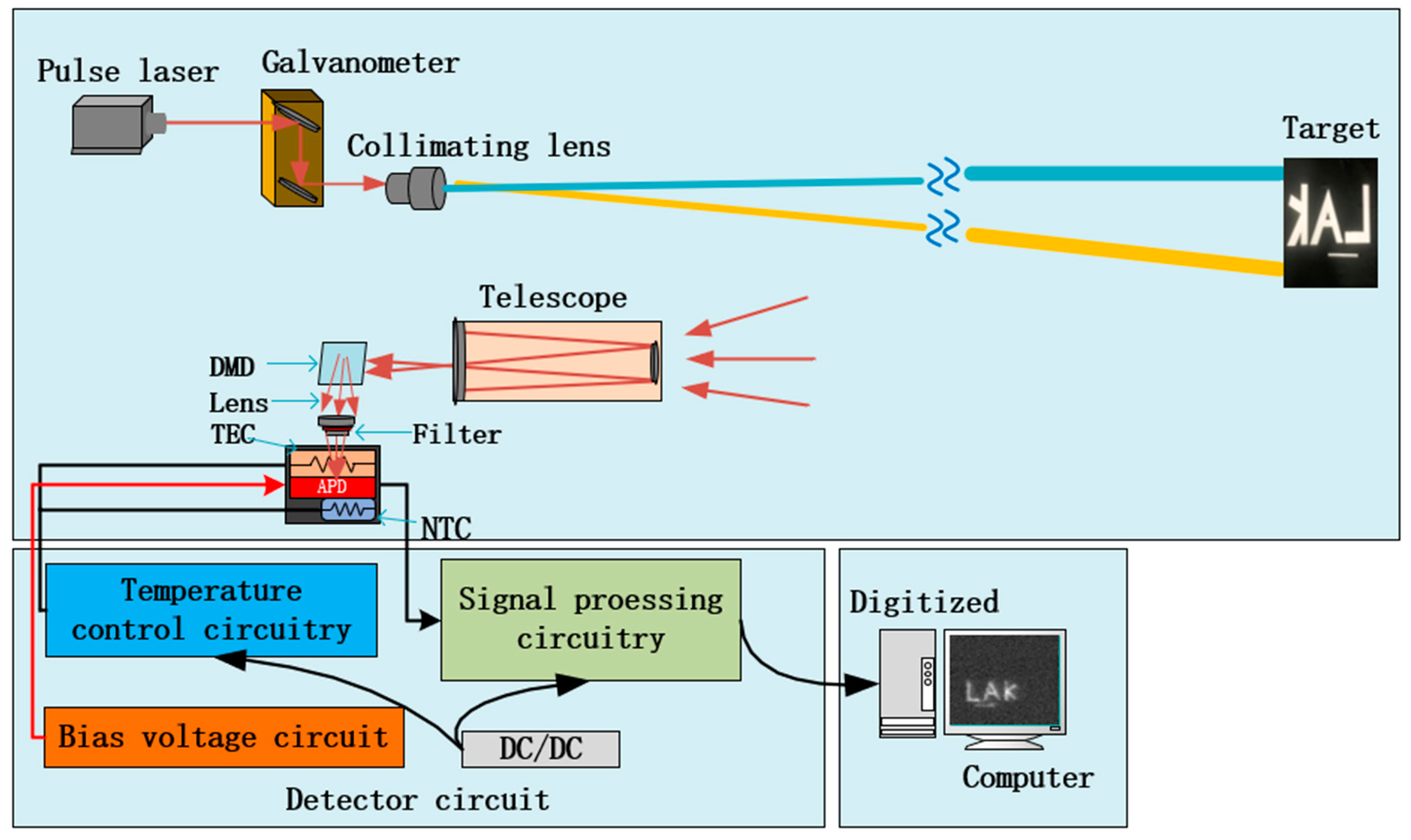
2. Single-Pixel Imaging Lidar System and Detector Circuit Design
2.1. Single-Pixel Imaging Lidar System
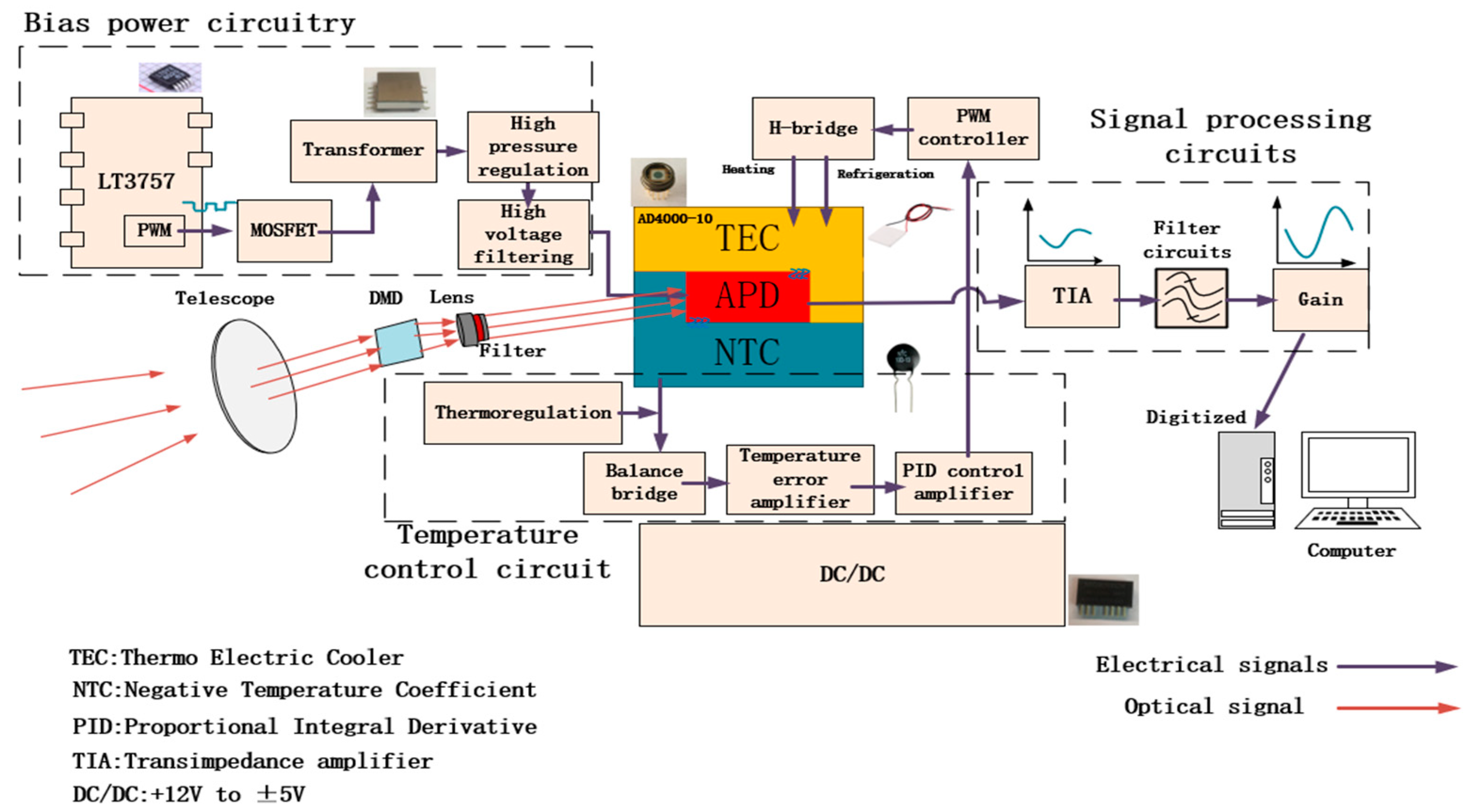
2.2. Detector Circuit
- (1)
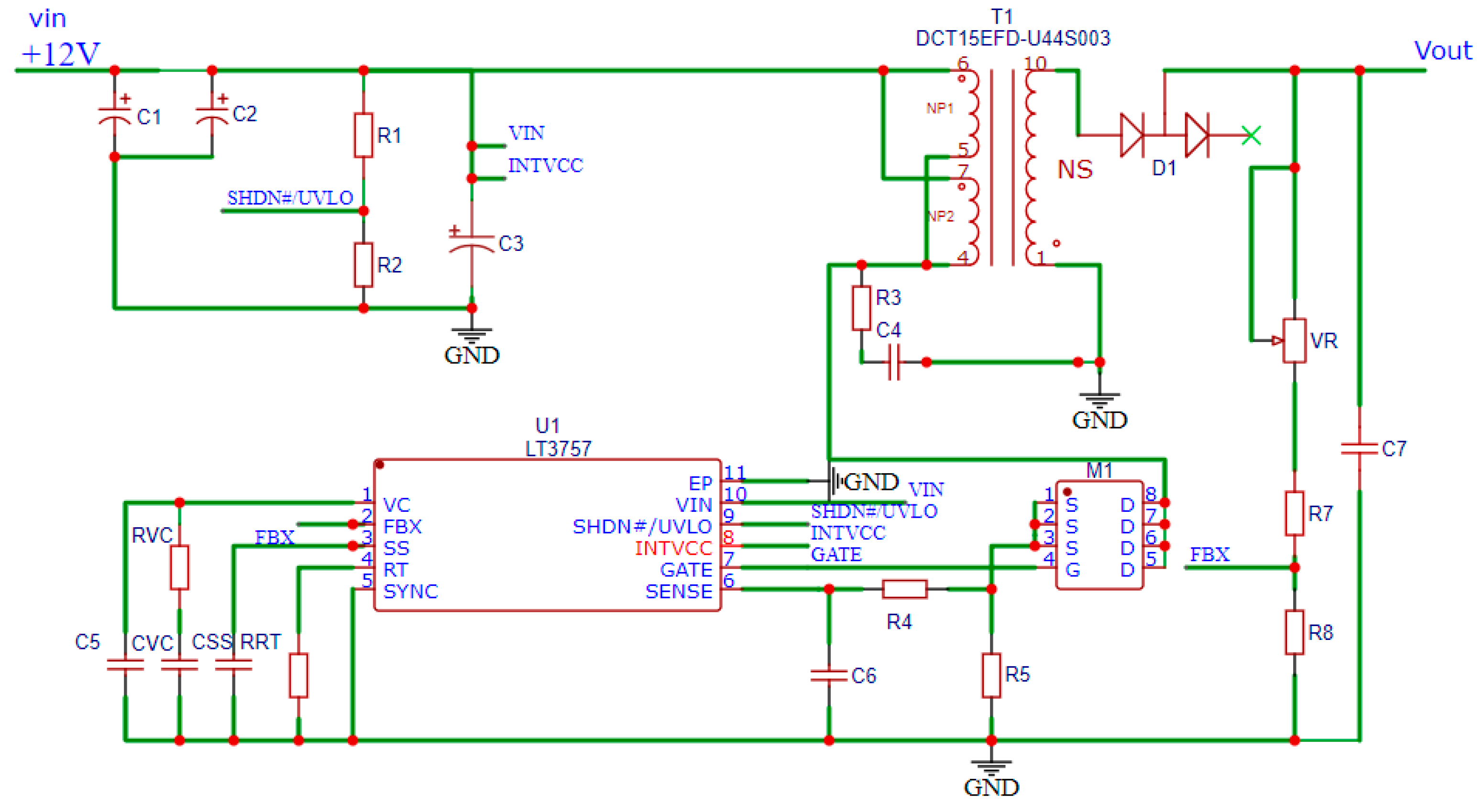
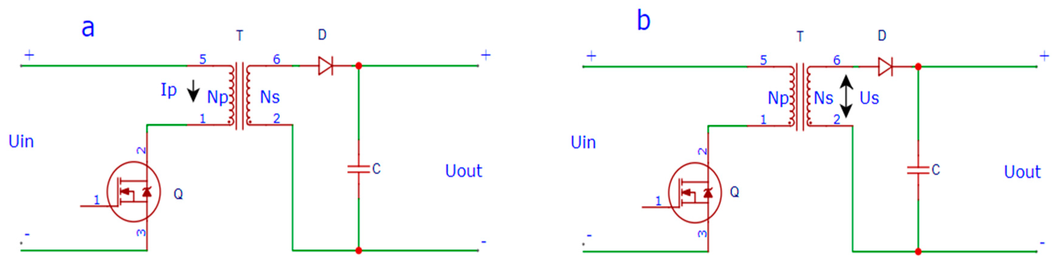
- Bias Power Circuit
- (2)
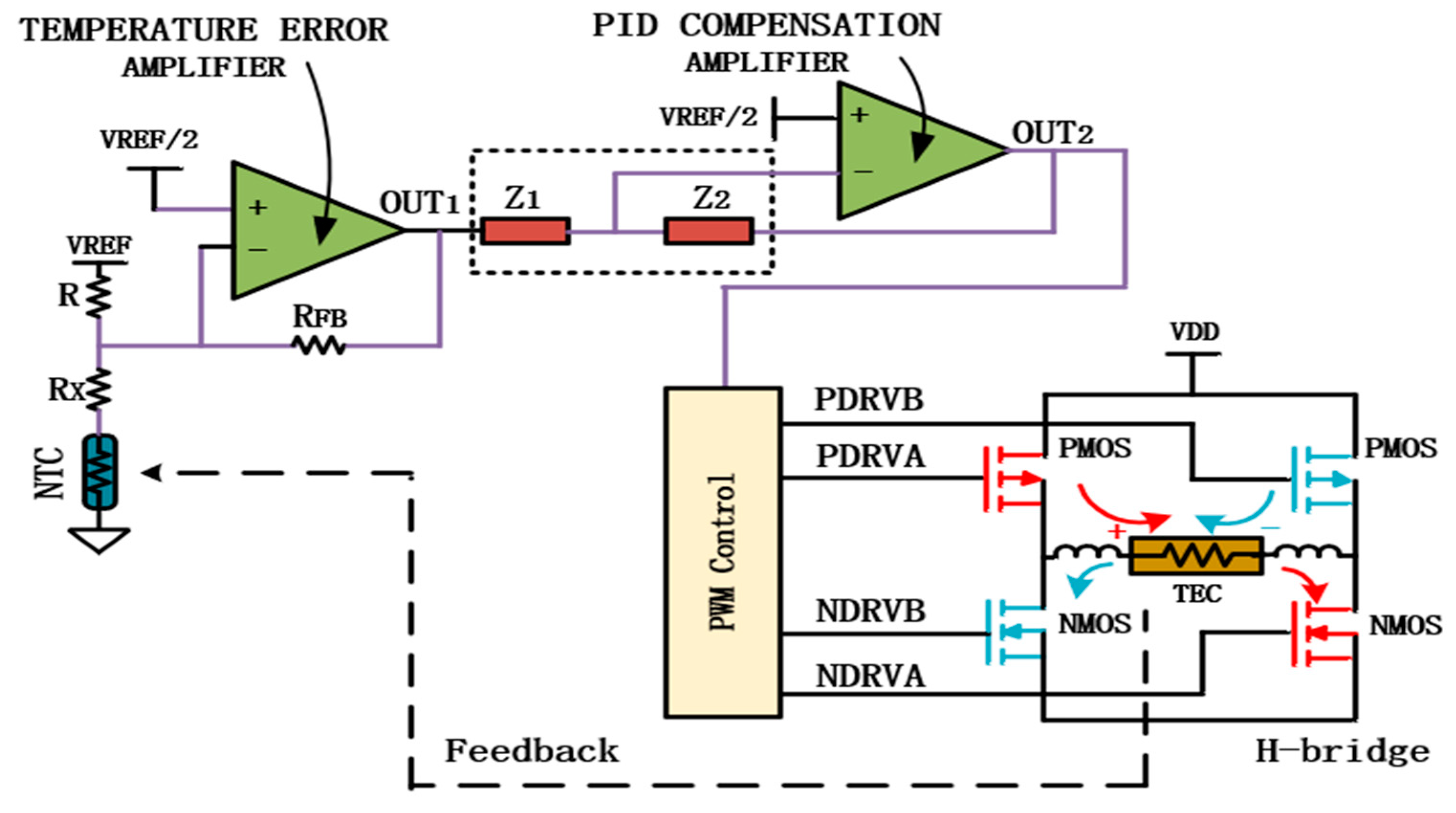
- Temperature Control Circuit
- (3)
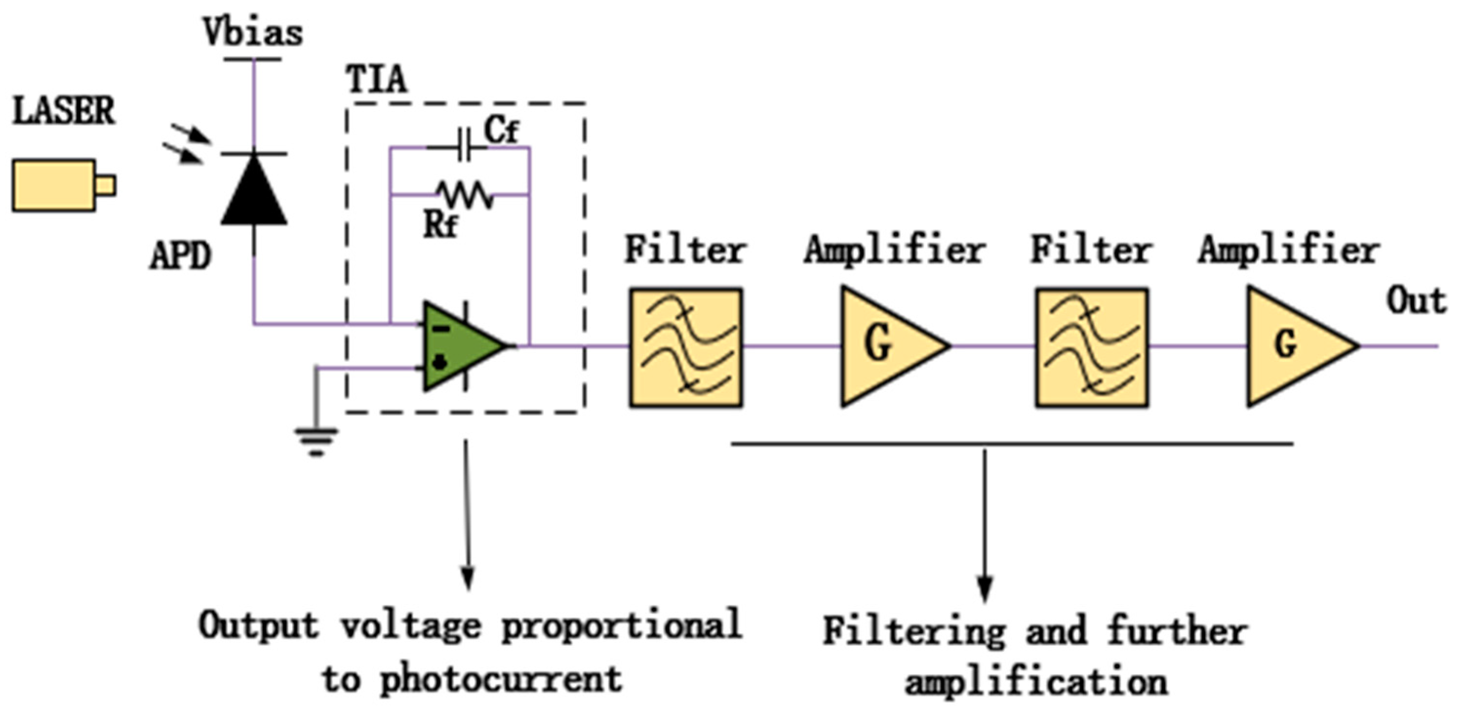
- Signal Processing Circuit
3. Results and Analysis
3.1. Circuit Design Test and Analysis
- (1)
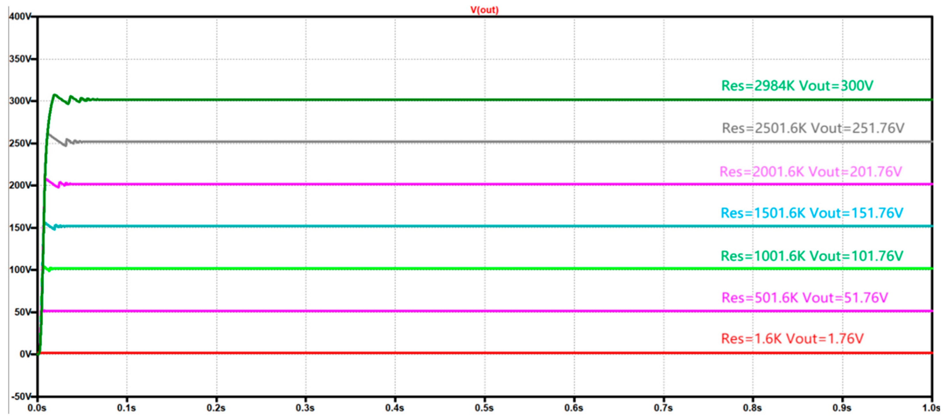
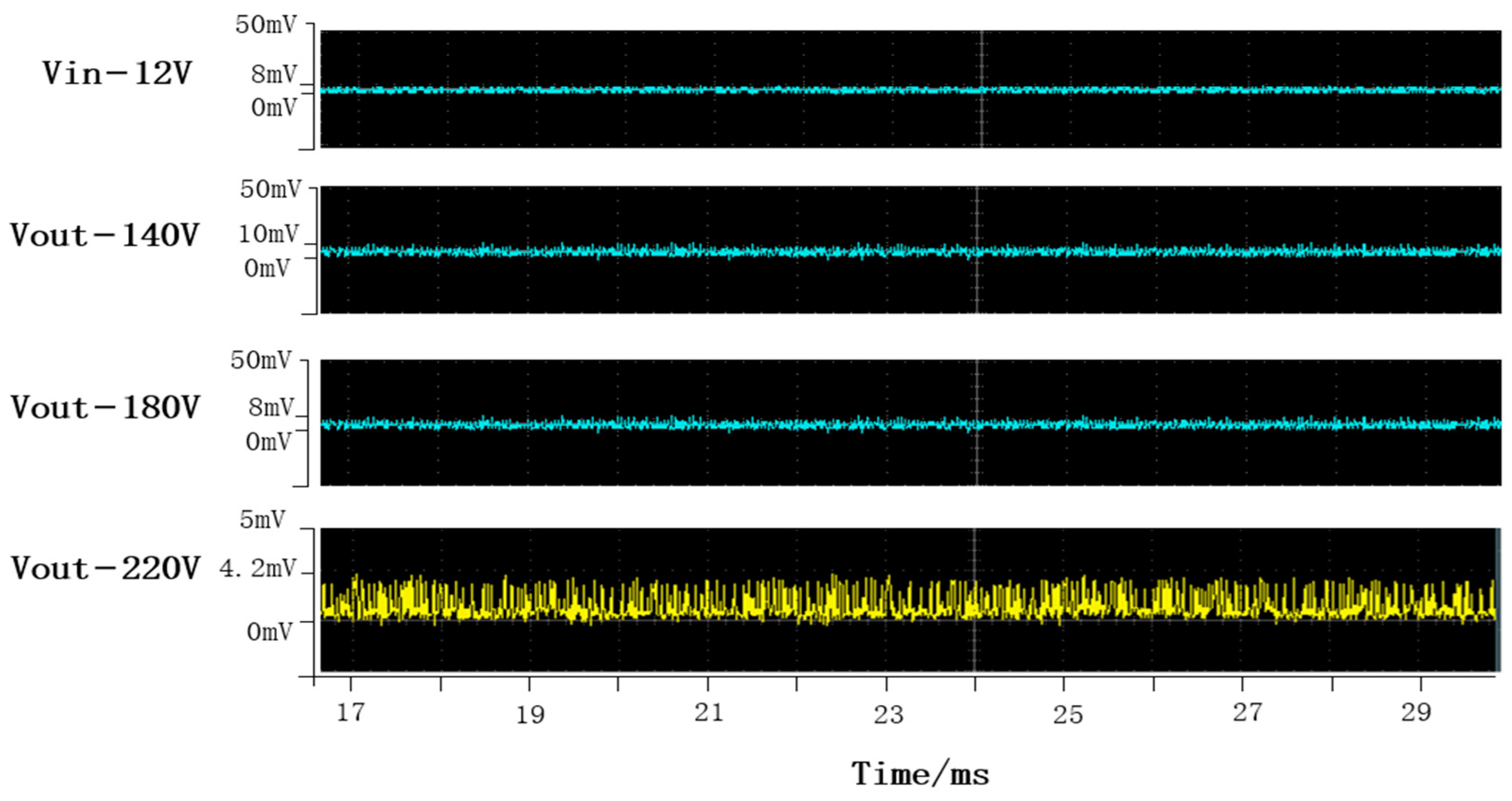
- Bias Power Test and Analysis
- (2)
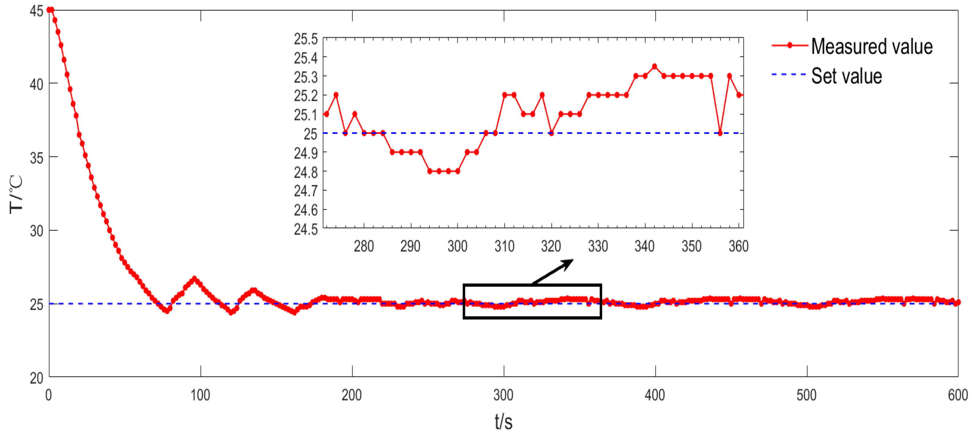
- Temperature Control Test and Analysis
3.2. Detector Test and Analysis
4. Conclusions
- (1)
- The bias voltage circuit was simulated and tested through circuit simulation software, suggesting that the output voltage ranged from DC 1.76 V to 300 V. When the actual output DC was 140 V, 180 V and 220 V, the output transient voltage ripple was less than 0.01% of the output voltage, which satisfied the voltage ripple requirement of most APDs.
- (2)
- The temperature control unit sensed the ambient temperature of APD through NTC, the differential operational amplifier and PID network compensated the temperature error, and the pulse regulation drive controller changed the TEC working mode, making the ambient temperature stable at 25 ± 0.3 °C within 5 h and eliminating the effects of temperature drift on APD breakdown voltage, quantum efficiency, dark current and other parameters.
- (3)
- The signal processing unit was designed with a multi-cascade amplification cascade structure to convert and amplify weak signals. The filtering circuit between two cascades effectively filtered out the interference brought by noise and improved the signal-to-noise ratio of the detector.
- (4)
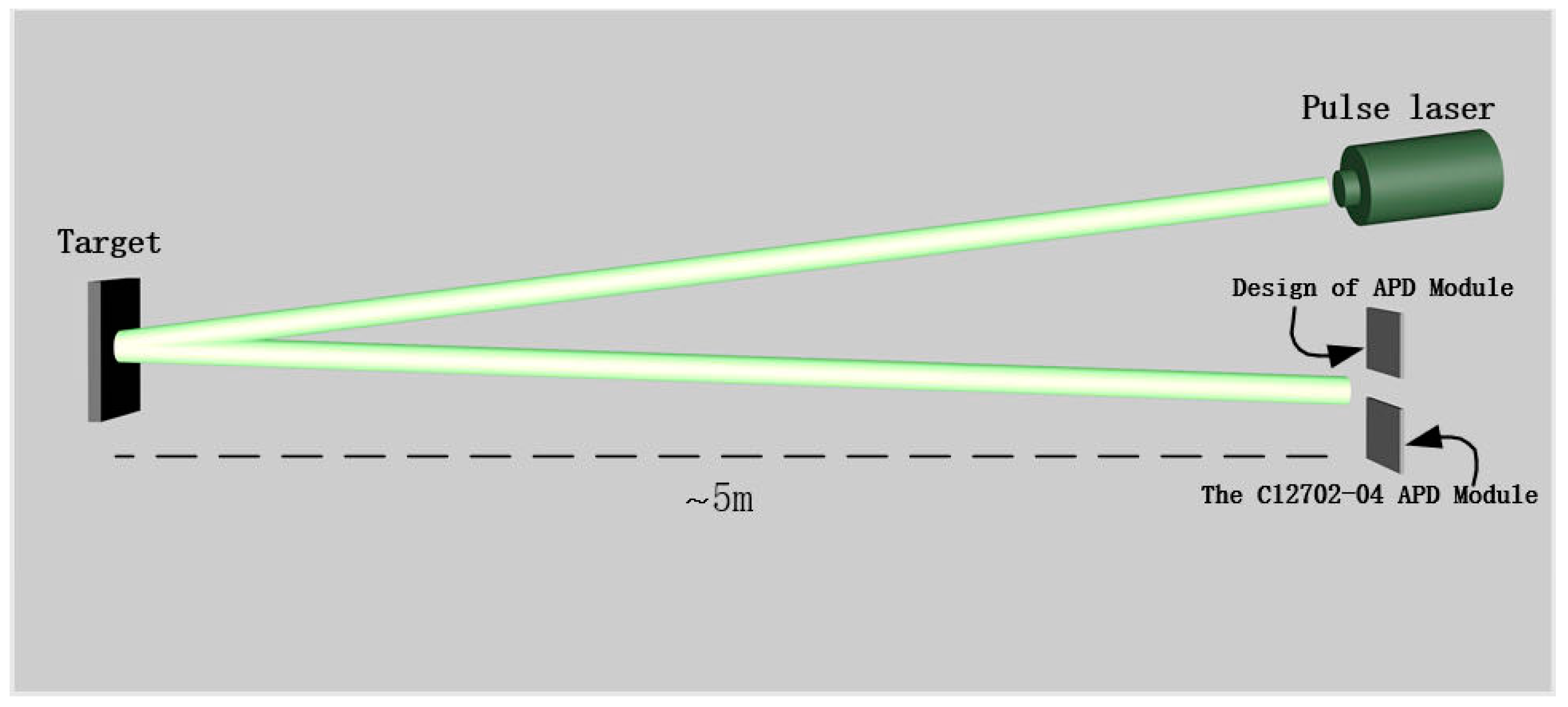
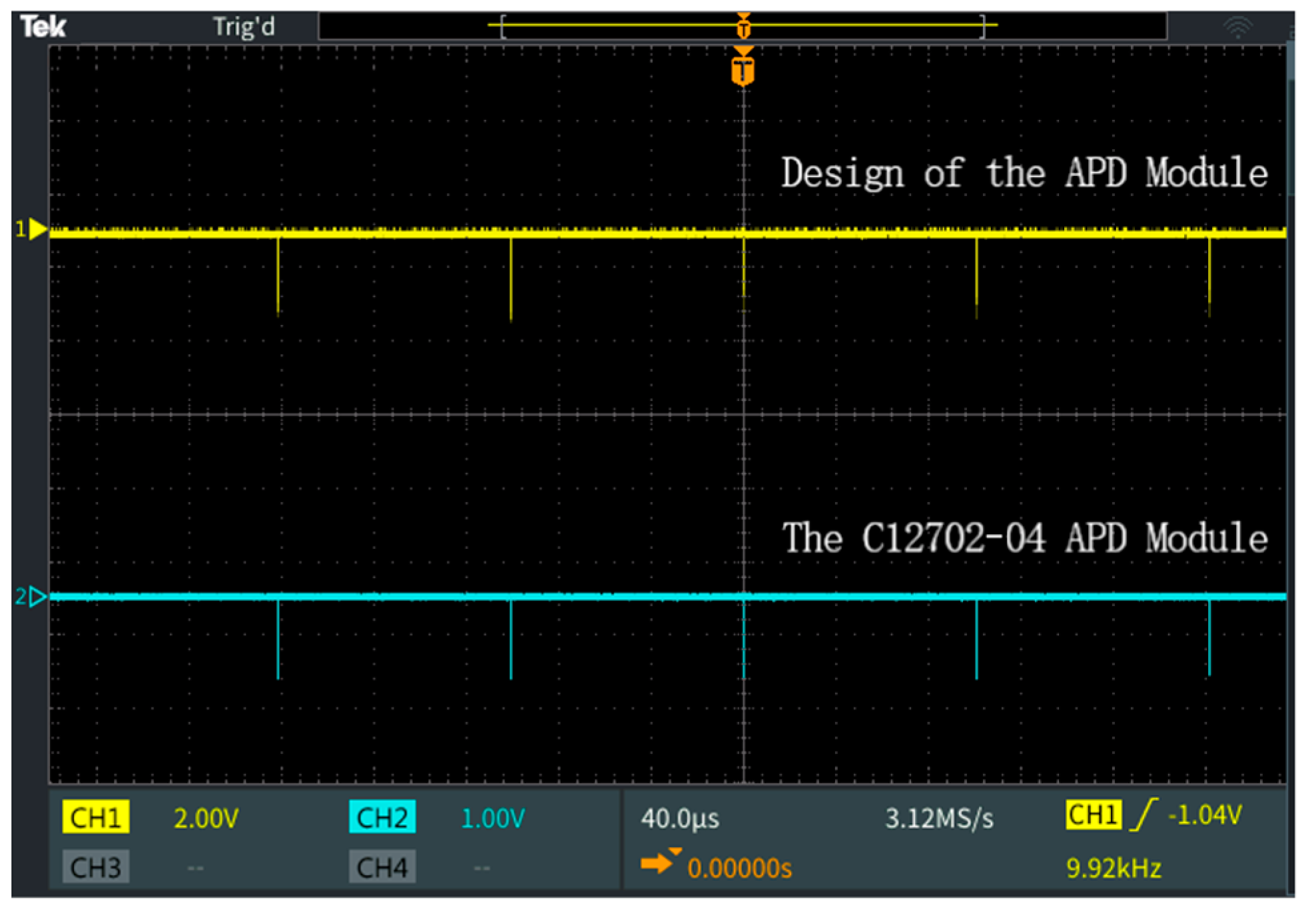
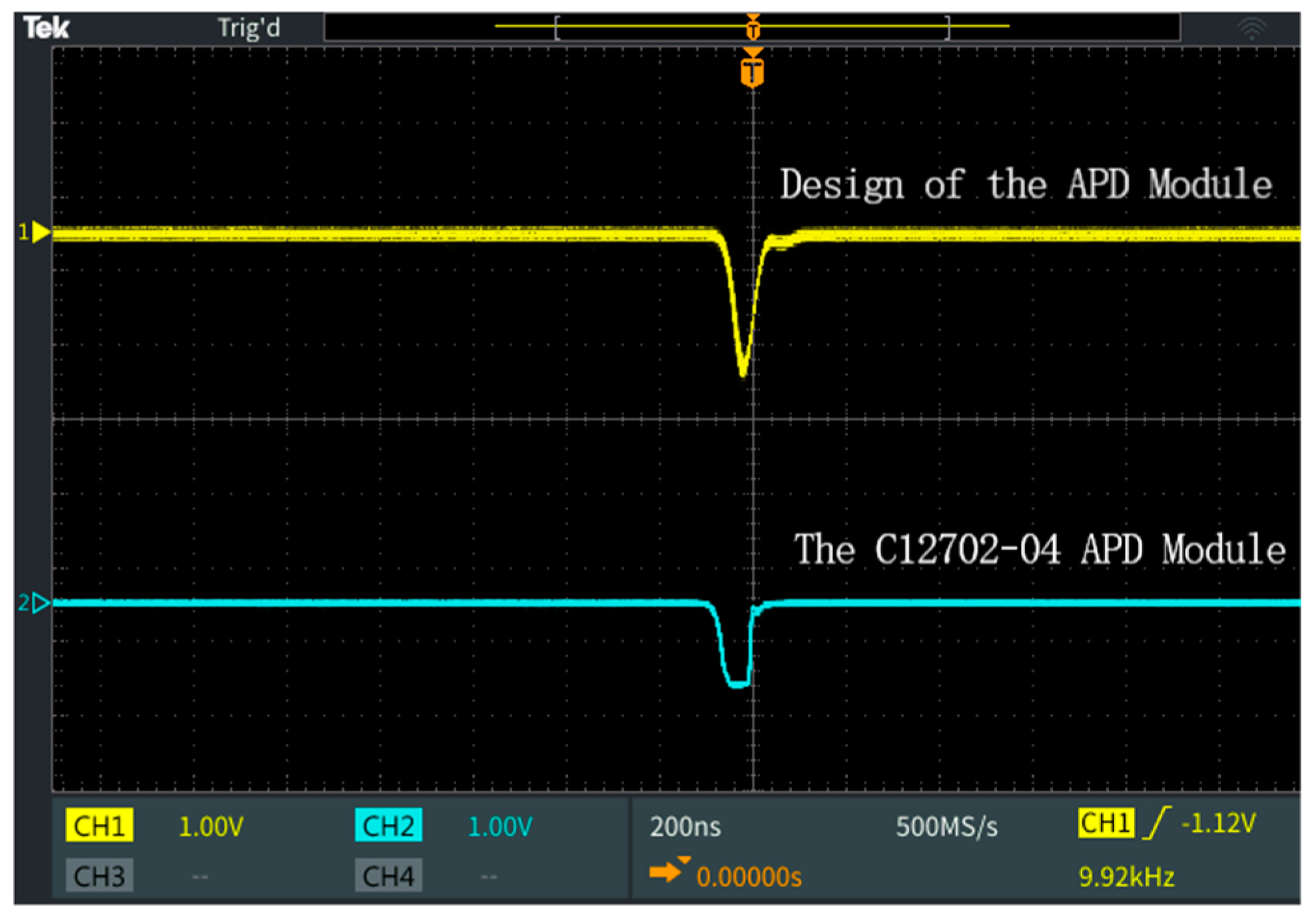
- In the test experiment carried out in the laboratory with the light scattering signal of the pulsed laser as the signal source, the encapsulated APD detector was in good agreement with the commercial Licel detector on the heavy frequency and pulse width response of the scattering signal.
- (5)
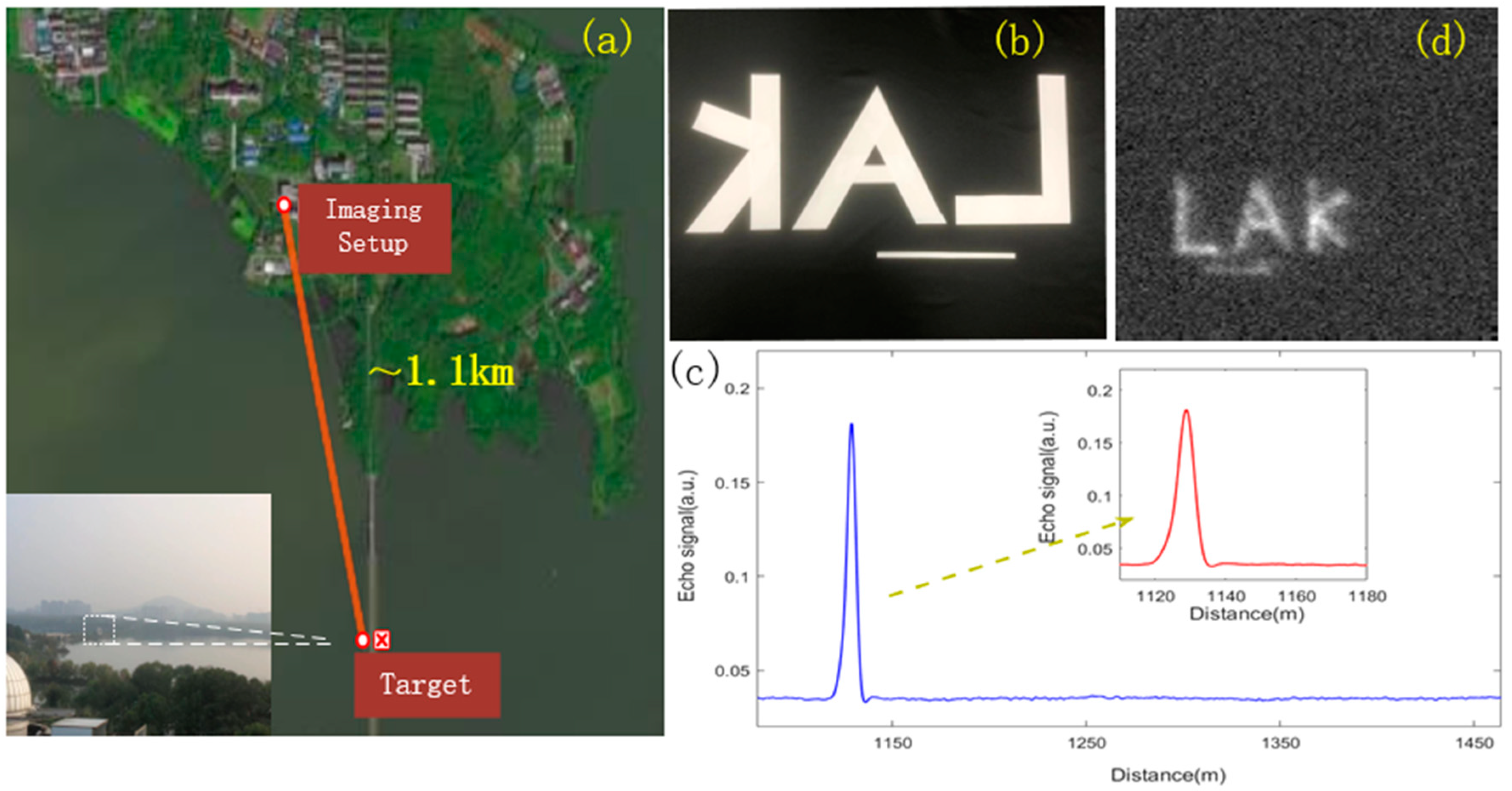
- The encapsulated APD detector was applied to a near-infrared single-pixel imaging lidar system in the real atmospheric environment, and a laser backscattered signal of 1.5 km was obtained. The imaging experiment was carried out on the letter puzzle target about 1.1 km away from the laser transmitting end, and the target image was recovered by utilizing the basic principle of single-pixel imaging, which further verified the stability and reliability of the encapsulated APD detector by comparing with the physical image.
Author Contributions
Funding
Institutional Review Board Statement
Informed Consent Statement
Data Availability Statement
Conflicts of Interest
References
- Tian, Z.; Yang, G.; Zhang, Y.; Cui, Z.; Bi, Z. A range-gated imaging flash liDAR based on the adjacent frame difference method. Opt. Lasers Eng. 2021, 141, 106558. [Google Scholar] [CrossRef]
- Schwarz, B. Mapping the world in 3D. Nat. Photon 2010, 4, 429–430. [Google Scholar] [CrossRef]
- Carter, W.E.; Glennie, C.L.; Shrestha, R.L. Geodetic Imaging by Airborne liDAR: A Golden Age in Geodesy—A Bonanza for Related Sciences; Springer: Cham, Switzerland, 2015. [Google Scholar]
- Gschwendtner, A.B.; Keicher, W.E. Development of Coherent Laser Radar at Lincoln Laboratory. Linc. Lab. J. 2000, 12, 383–396. [Google Scholar]
- Shi, D.; Huang, J.; Meng, W.; Yin, K.; Sun, B.; Wang, Y.; Yuan, K.; Xie, C.; Liu, D.; Zhu, W. Radon single-pixel imaging with projective sampling. Opt. Express 2019, 27, 14594–14609. [Google Scholar]
- Zha, L.; Shi, D.; Huang, J.; Yuan, K.; Meng, W.; Yang, W.; Jiang, R.; Chen, Y.; Wang, Y. Single-pixel tracking of fast-moving object using geometric moment detection. Opt. Express 2021, 29, 30327–30336. [Google Scholar] [CrossRef]
- Yang, H.; Fang, Z.; Cao, Y.; Xie, C.; Zhou, T.; Wang, B.; Xing, K.; Lolli, S. Impacts of Transboundary Dust Transport on Aerosol Pollution in the Western Yangtze River Delta Region, China: Insights Gained From Ground-Based liDAR and Satellite Observations. Earth Space Sci. 2021, 8, 3. [Google Scholar] [CrossRef]
- Comerón, A.; Muñoz-Porcar, C.; Rocadenbosch, F.; Rodríguez-Gómez, A.; Sicard, M. Current Research in liDAR Technology Used for the Remote Sensing of Atmospheric Aerosols. Sensors 2017, 17, 1450. [Google Scholar] [CrossRef]
- Shi, D.; Yin, K.; Huang, J.; Yuan, K.; Zhu, W.; Xie, C.; Liu, D.; Wang, Y. Fast tracking of moving objects using single-pixel imaging. Opt. Commun. 2019, 440, 155–162. [Google Scholar] [CrossRef]
- Zhang, P.; Zhou, J. Single photon detector and its development. Sens. World 2003, 10, 6–10. [Google Scholar] [CrossRef]
- Moll, J.L.; Tanenbaum, M.; Goldey, J.M.; Holonyak, N. P-N-P-N Transistor switches. Proc. IRE 1956, 44, 1174–1182. [Google Scholar] [CrossRef]
- Song, D.; Wang, X. APD, PMT and Hybrid Photodetectors With High-End Sensitivity. Semicond. Technol. 2000, 3, 5–8+12. [Google Scholar]
- Wirth, W.F. High-speed snubberless operation of GTOs using a new gate drive technique. IEEE Trans. Ind. Appl. 1988, 24, 127–131. [Google Scholar] [CrossRef]
- Fei, W. The Study of Framework of Data Acquisition System for Lidar. Ph.D. Thesis, University of Science and Technology of China, Anhui, China, 2013. [Google Scholar]
- Lei, Z. Principle and application of photodetector. Physics 1994, 4, 220–226. [Google Scholar]
- Wu, J.; Yu, X.; Shi, S.; Zheng, L.; Sun, W. Infrared ranging technology by using single photon APD array readout integrated circuit. Infrared Laser Eng. 2017, 46, 604002. [Google Scholar]
- Wang, F.; Tang, W.; Wang, T.; Gou, J. Design of 3D laser imaging receiver based on 8 × 8 APD detector array. Chin. Opt. 2015, 8, 422–427. [Google Scholar] [CrossRef]
- Shi, Y.; Zhu, H.; Yang, X.; Zeng, H.; Li, Z.; Liu, C.; Wang, J.; Wang, W. InP-based free running mode single photon avalanche photodiode. Infrared Laser Eng. 2020, 49, 0103005. [Google Scholar]
- Zhang, H.; Wang, L.; Wu, C.; Wang, Y.; Yang, L.; Pan, H.; Liu, Q.; Guo, X.; Tang, K.; Zhang, Z.; et al. Avalanche photodiode single-photon detector with high time stability. Acta Phys. Sin. 2020, 69, 074204. [Google Scholar] [CrossRef]
- Tao, J. High performance superlattice avalanche photodiodes for ultra-high speed optical communications. Infrared 1998, 7, 40. [Google Scholar]
- Zheng, R.; Wu, G. Pulsed one-dimensional scannerless LiDAR system based on linear APD array. Infrared Laser Eng. 2012, 41, 96–100. [Google Scholar]
- Wang, S.; Sun, H.; Zhao, Y.; Zeng, H.; Liu, T. Method of improving 3D imaging resolution of APD array based on optical phased array. Infrared Laser Eng. 2019, 48, 406003. [Google Scholar] [CrossRef]
- Sun, M.; Yan, S.; Wang, S. Reconstruction Algorithms for Ghost Imaging and Single-Pixel Imaging. Adv. Laser Optoelectron. 2022, 59, 0200001. [Google Scholar]
- Zhang, Z.; Ma, X.; Zhong, J. Single-pixel imaging by means of Fourier spectrum acquisition. Nat. Commun. 2015, 6, 6225. [Google Scholar] [CrossRef] [PubMed]
- Zuo, W.; Zhu, Y.; Qiu, M.; Liu, J.; Chen, W. Influence of performances of APD detector on CO2 concentration error retrieved by liDAR measurement. Infrared Laser Eng. 2018, 47, 406002. [Google Scholar]
- Gu, W. Research on Optimization Design and Application of Flyback High Frequency Transformer. Ph.D. Thesis, Nanchang University, Nanchang, China, 2019. [Google Scholar]
- Jie, X. Research and Improvement of Cross-regulation Rate of Multi-output Flyback Switching Power Supply. Ph.D. Thesis, Huazhong University of Science & Technology, Wuhan, China, 2019. [Google Scholar]
- Wang, Q.; Wang, H.; Tian, H. Design and Simulation of a Flyback Switching Power Supply. Comput. Simul. 2021, 38, 83–88+138. [Google Scholar]
- Zhang, P.; Zhang, L. A Semiconductor Laser’s Temperature Control System Based on PID Algorithm. Electron. Sci. Technol. 2016, 03, 543–545. [Google Scholar]
- Liu, F.; Zhang, X.; Jia, Y. Design of closed-loop temperature controlled APD photoelectric detector. Transducer Microsyst. Technol. 2016, 35, 97–99+106. [Google Scholar]
- Li, X.; Peng, H.; Wang, C. APD optimal gain control investigation for spaceborne laser range finder. Infrared Laser Eng. 2016, 45, 77–82. [Google Scholar]
- Huang, J.; Shang, L.; Ma, S.; Zhang, S.; Liu, Q.; Hou, Y.; Kong, Q.; Xu, B. Research Progress on Impact Factors to Output Power of Semiconductor Laser. Mater. China 2021, 40, 218–224. [Google Scholar]
- Huang, J.; Li, Z.; Shi, D.; Chen, Y.; Yuan, K.; Hu, S.; Wang, Y. Scanning single-pixel imaging liDAR. Opt. Express 2022, 30, 37484–37492. [Google Scholar] [CrossRef]
- Froehly, L.; Martin, S.N.; Lasser, T.; Depeursinge, C.; Lang, F. Erratum to: “Multiplexed 3D imaging using wavelength encoded spectral interferometry: A proof of principle” [Optics Communications 222 (2003) 127–136]. Opt. Commun. 2003, 224, 127–136. [Google Scholar] [CrossRef]


| Symbol | Characteristic | Test Condition | Min. | Type | Max. | Unit |
|---|---|---|---|---|---|---|
| Active area | Φ 4000 | um | ||||
| Dark current | M = 100 | 50 | 500 | nA | ||
| C | Responsivity | M = 100; λ = 1064 nm | 49 | A/W | ||
| Rise time | M = 100; λ = 1064 nm; = 50 Ω | 6 | ns | |||
| Cut-off frequency | −3 dB | 70 | MHz | |||
| Breakdown voltage | = 2 uA | 200 | 300 | 600 | V | |
| Type No. | Photosensitive Area | Supply Voltage | Spectral Response Range | Frequency Bandwidth −3 dB | ||
|---|---|---|---|---|---|---|
| Min. | Typ. | Max. | ||||
| C12702-04 | Φ 3.0 mm | +4.75 | +5 | +5.25 | 400 to 1100 (nm) | 4 kHz–80 MHz |
| Section | Parameter | Numeric Value | Section | Parameter | Numeric Value |
|---|---|---|---|---|---|
| Laser emission unit | Laser line | λ = 1064 nm | Signal acquisition unit Control unit/procedure | High-speed digital card/bandwidth | 400 MHz |
| Pulse repetition frequency | 400 Hz | ||||
| Maximum pulse energy | 400 mJ | ||||
| Signal reception unit | Galvanometer scanned area | ±0.393 rad | DMD pattern Galvanometer acquisition card Synchronizing signal… | - | |
| Telescopic aperture/focal length | Φ = 240 mm | - | |||
| 730 mm | - | ||||
| DMD mirror array /dimension | 1920 × 1200 | - | |||
| 20.7 × 13.5 mm | - |
Disclaimer/Publisher’s Note: The statements, opinions and data contained in all publications are solely those of the individual author(s) and contributor(s) and not of MDPI and/or the editor(s). MDPI and/or the editor(s) disclaim responsibility for any injury to people or property resulting from any ideas, methods, instructions or products referred to in the content. |
© 2023 by the authors. Licensee MDPI, Basel, Switzerland. This article is an open access article distributed under the terms and conditions of the Creative Commons Attribution (CC BY) license (https://creativecommons.org/licenses/by/4.0/).
Share and Cite
Lv, A.; Yuan, K.; Huang, J.; Shi, D.; Zhang, S.; Chen, Y.; He, Z. Integrated Encapsulation and Implementation of a Linear-Mode APD Detector for Single-Pixel Imaging Lidar. Photonics 2023, 10, 970. https://doi.org/10.3390/photonics10090970
Lv A, Yuan K, Huang J, Shi D, Zhang S, Chen Y, He Z. Integrated Encapsulation and Implementation of a Linear-Mode APD Detector for Single-Pixel Imaging Lidar. Photonics. 2023; 10(9):970. https://doi.org/10.3390/photonics10090970
Chicago/Turabian StyleLv, Akang, Kee Yuan, Jian Huang, Dongfeng Shi, Shiguo Zhang, Yafeng Chen, and Zixin He. 2023. "Integrated Encapsulation and Implementation of a Linear-Mode APD Detector for Single-Pixel Imaging Lidar" Photonics 10, no. 9: 970. https://doi.org/10.3390/photonics10090970