Evanescent Wave Sensitivity of Silica-Titania Rib Waveguides in the Single-Mode Propagation Regime


Abstract
:1. Introduction
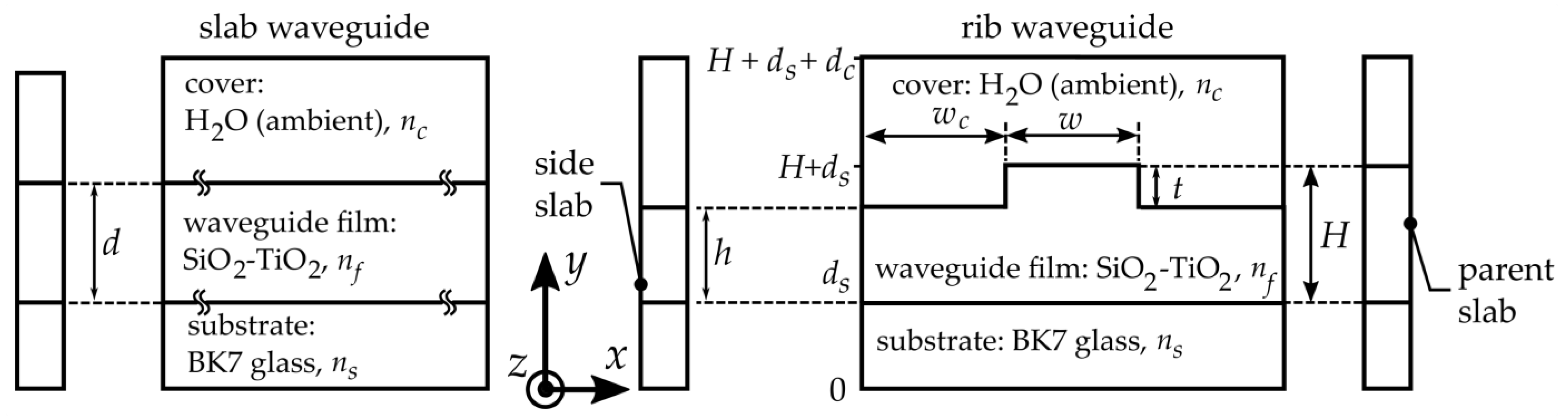
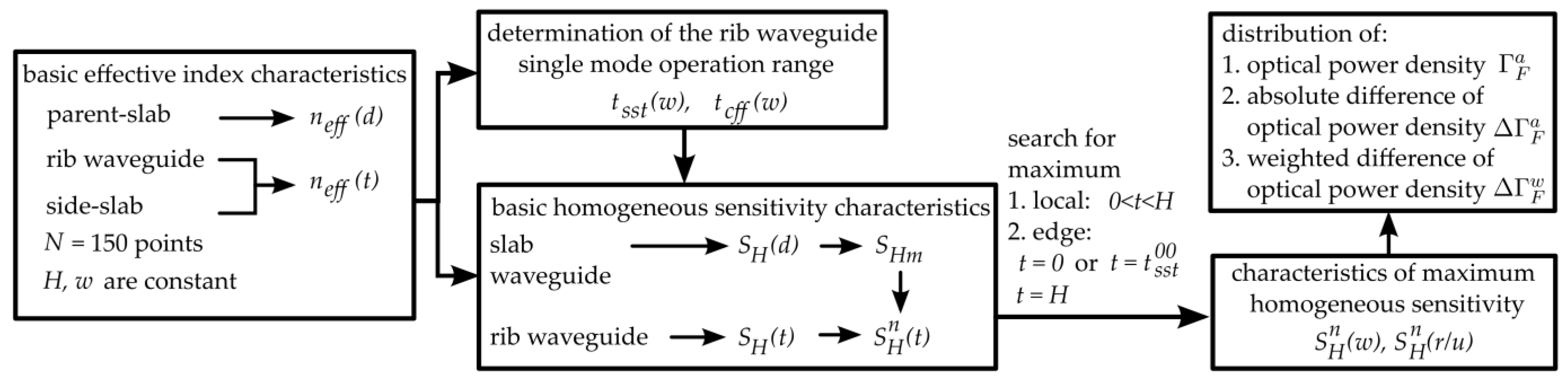
2. Structure and Methods
3. Results
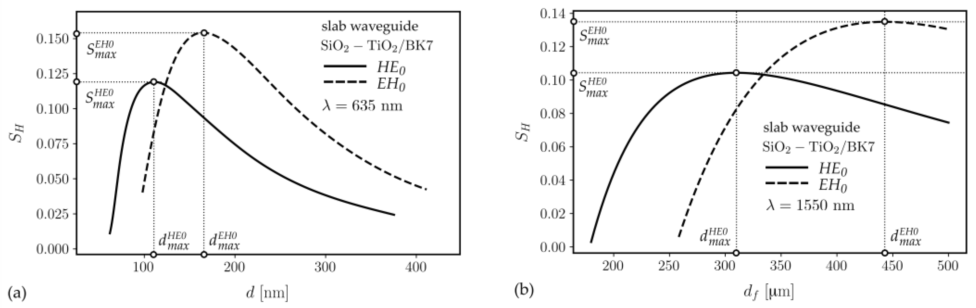
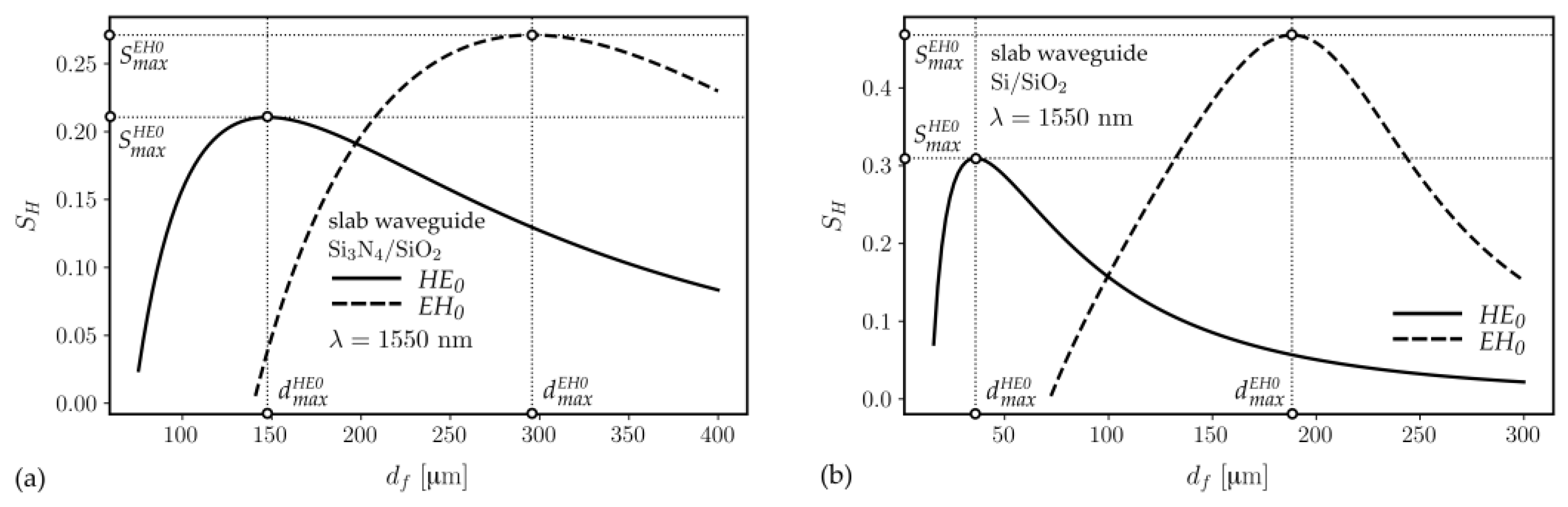
3.1. Parent Slab Waveguide
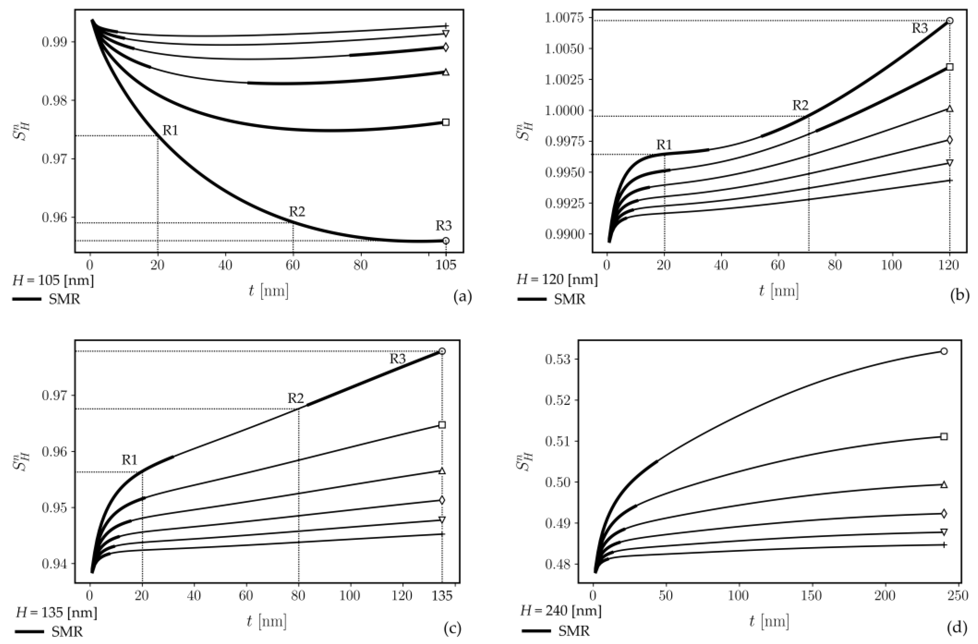
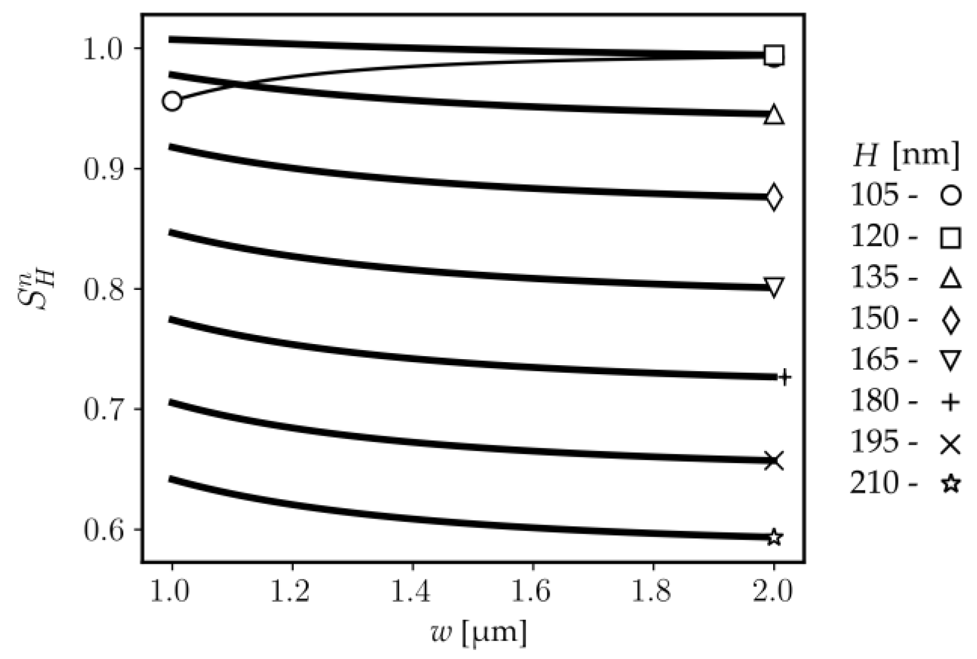
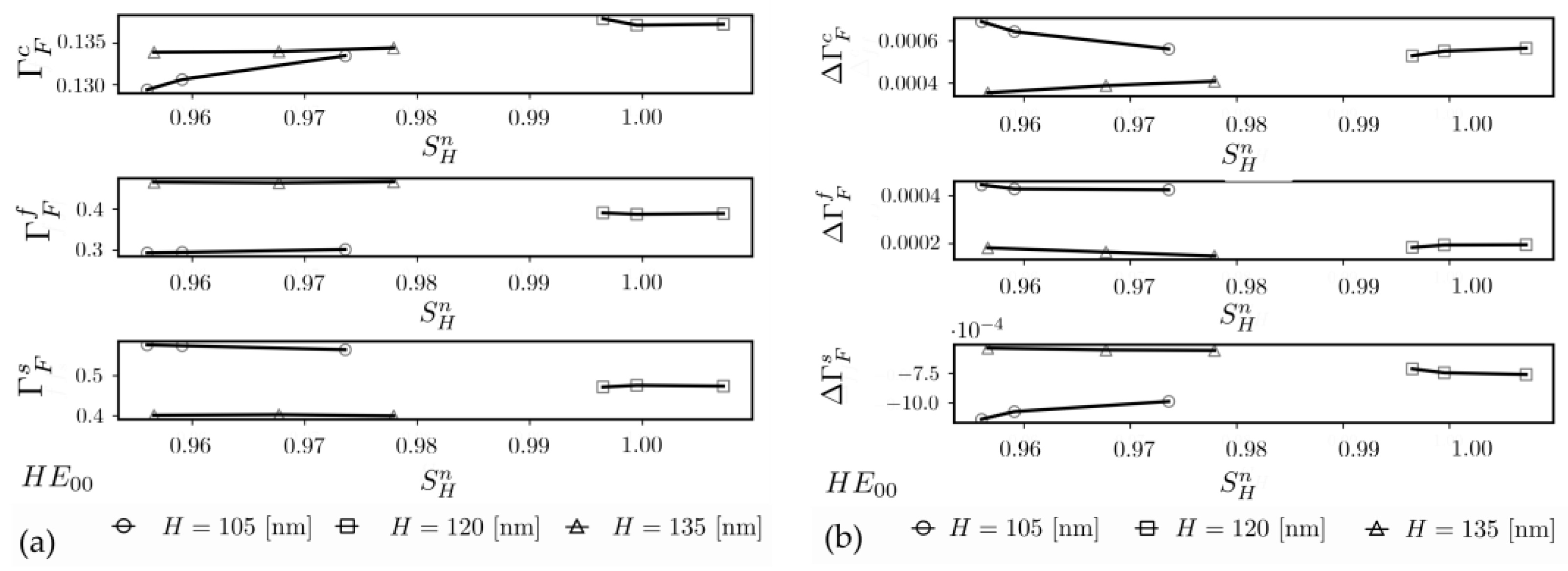
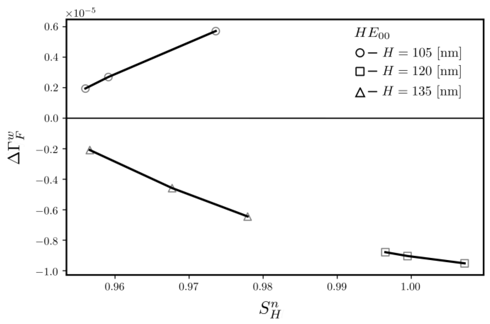
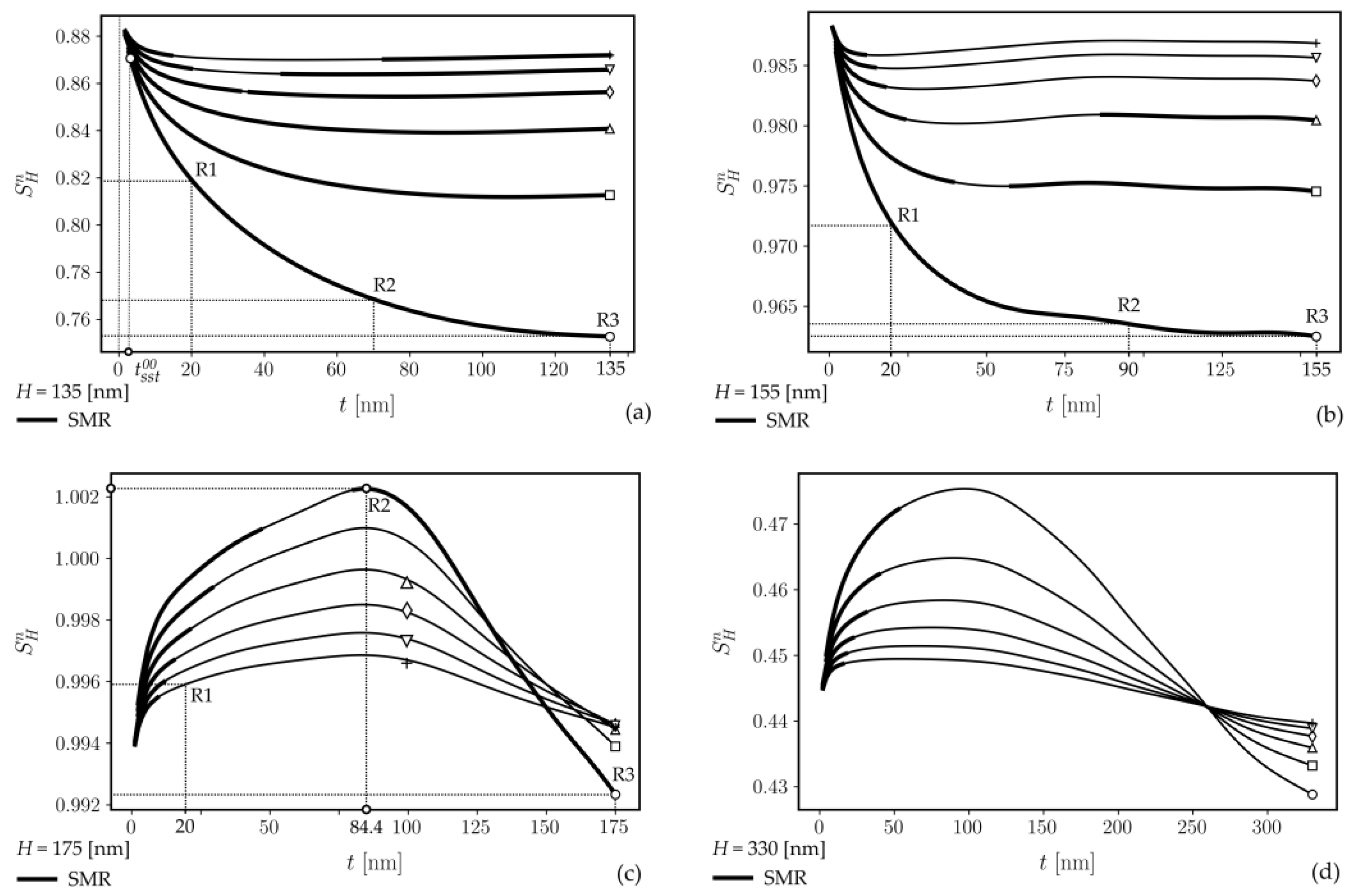
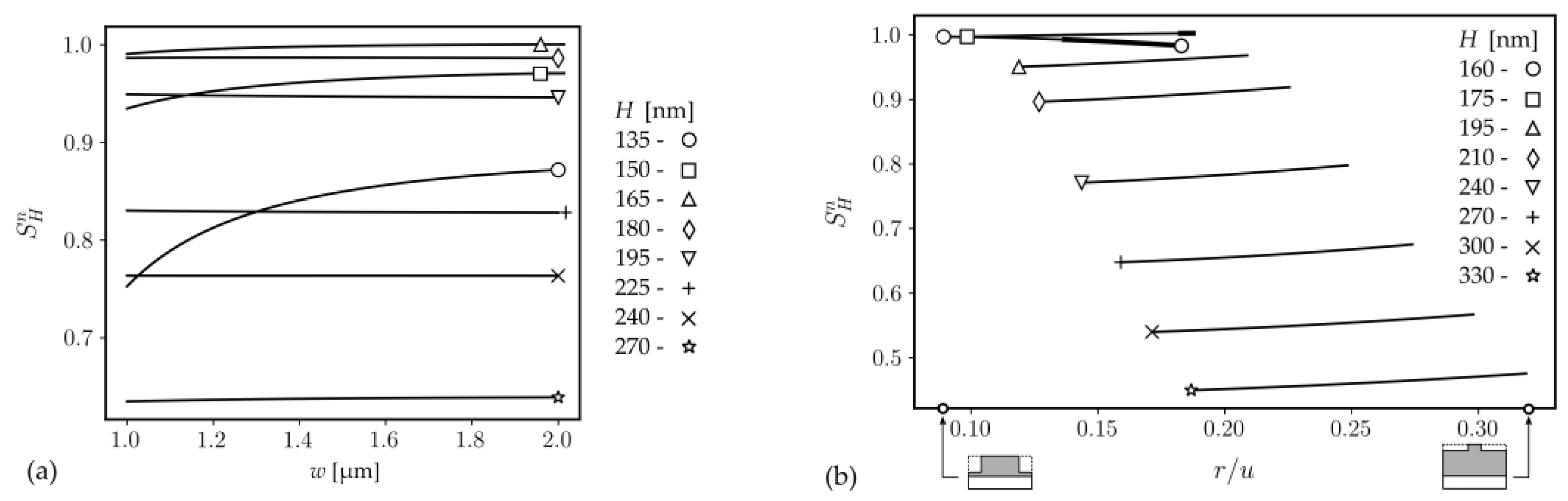
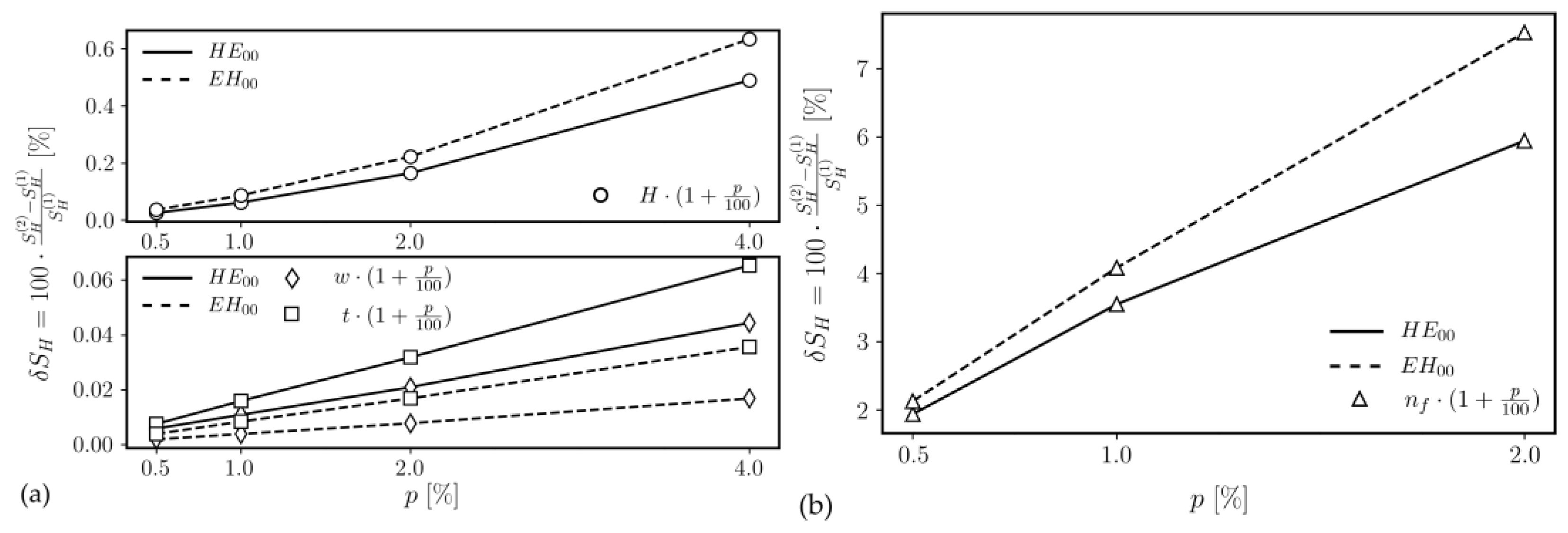
3.2. Rib Waveguide—Fundamental HE Modes
3.3. Rib Waveguide—Fundamental HE Modes
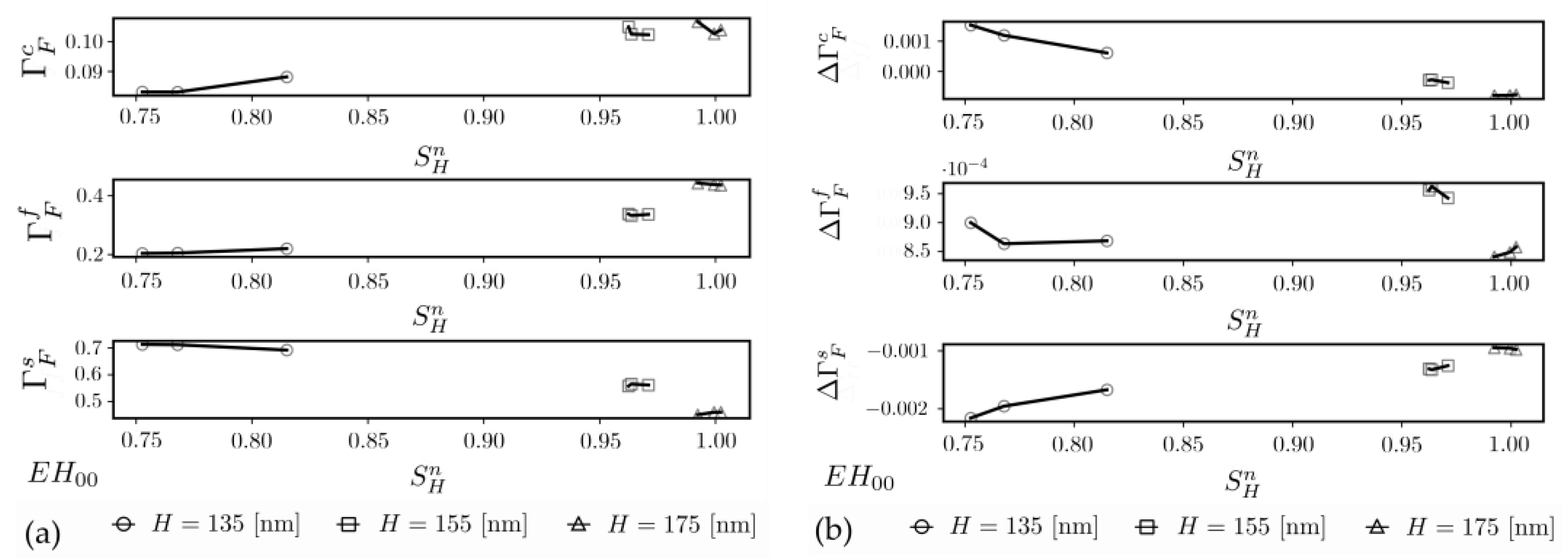
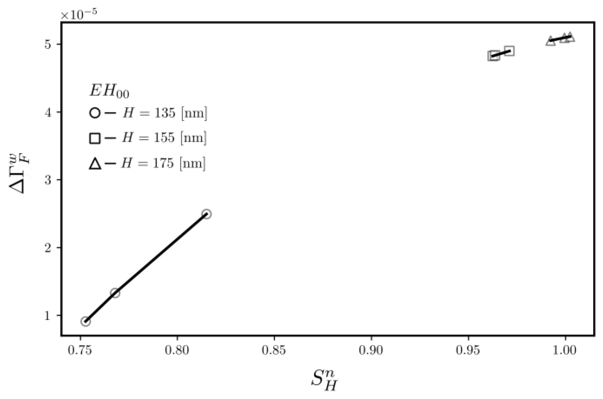
4. Discussion
5. Conclusions
Author Contributions
Funding
Institutional Review Board Statement
Informed Consent Statement
Data Availability Statement
Conflicts of Interest
References
- Lipka, T.; Moldenhauer, L.; Müller, J.; Trieu, H.K. Photonic integrated circuit components based on amorphous silicon-on-insulator technology. Photonics Res. 2016, 4, 126–134. [Google Scholar] [CrossRef]
- Swagata, S.; Pradip, D.K.; Pallab, B.; Pranabendu, G. A 1 × 2 polarization-independent power splitter using three-coupled silicon rib waveguides. J. Opt. 2018, 20, 095801. [Google Scholar] [CrossRef]
- Ottaviano, L.; Pu, M.; Semenova, E.; Yvind, K. Low-loss high-confinement waveguides and microring resonators in AlGaAs-on-insulator. Opt. Lett. 2016, 41, 3996–3999. [Google Scholar] [CrossRef] [PubMed]
- Blumenthal, D.J.; Heideman, R.; Geuzebroek, D.; Leinse, A.; Roeloffzen, C. Silicon nitride in silicon photonics. Proc. IEEE 2018, 106, 2209–2231. [Google Scholar] [CrossRef]
- Özden, A.; Demirtas, M.; Ay, F. Polarization insensitive single mode Al2O3 rib waveguide design for applications in active and passive optical waveguides. J. Eur. Opt. Soc.-Rapid 2015, 10, 15005. [Google Scholar] [CrossRef]
- Karasiński, P.; Tyszkiewicz, C.; Rogoziński, R. Optical channel structures based on sol-gel derived waveguide films. Opt. Appl. 2011, XLI, 351–357. [Google Scholar]
- Karasiński, P.; Kaźmierczak, A.; Zięba, M.; Tyszkiewicz, C.; Wojtasik, K.; Kielan, P. Highly Sensitive Sensor Structure Based on Sol-Gel Waveguide Films and Grating Couplers. Electronics 2021, 10, 1389. [Google Scholar] [CrossRef]
- Kang, J.; Takenaka, M.; Takagi, S. Novel Ge waveguide platform on Ge-on-insulator wafer for mid-infrared photonic integrated circuits. Opt. Express 2016, 24, 11855–11864. [Google Scholar] [CrossRef]
- Butt, M.A.; Tyszkiewicz, C.; Karasiński, P.; Zięba, M.; Hlushchenko, D.; Baraniecki, T.; Kazmierczak, A.; Piramidowicz, R.; Guzik, M.; Bachmatiuk, A. Development of a low-cost silica-titania optical platform for integrated photonics applications. Opt. Express 2022, 30, 23678–23694. [Google Scholar] [CrossRef]
- Butt, M.A.; Shahbaz, M.; Kozłowski, Ł.; Kaźmierczak, A.; Piramidowicz, R. Silica-Titania Integrated Photonics Platform-Based 1 × 2 Demultiplexer Utilizing Two Serially Cascaded Racetrack Microrings for 1310 nm and 1550 nm Telecommunication Wavelengths. Photonics 2023, 10, 208. [Google Scholar] [CrossRef]
- Butt, M.A.; Shahbaz, M.; Piramidowicz, R. Racetrack Ring Resonator Integrated with Multimode Interferometer Structure Based on Low-Cost Silica–Titania Platform for Refractive Index Sensing Application. Photonics 2023, 10, 978. [Google Scholar] [CrossRef]
- Kozma, P.; Kehl, F.; Ehrentreich-Förster, E.; Stamm, C.; Bier, F.F. Integrated planar optical waveguide interferometer biosensors: A comparative review. Biosens. Bioelectron. 2014, 58, 287–307. [Google Scholar] [CrossRef]
- Midwinter, J.E. On the use optical waveguide techniques for internal reflection spectroscopy. IEEE J. Quantum Electron. 1971, 7, 339–344. [Google Scholar] [CrossRef]
- Bastos, A.R.; Vicente, C.M.S.; Oliveira-Silva, R.; Silva, N.J.O.; Tacão, M.; da Costa, J.P.; Lima, M.; André, P.S.; Ferreira, R.A.S. Integrated Optical Mach-Zehnder Interferometer Based on Organic-Inorganic Hybrids for Photonics-on-a-Chip Biosensing Applications. Sensors 2018, 18, 840. [Google Scholar] [CrossRef]
- Lo, S.M.; Hu, S.; Gaur, G.; Kostoulas, Y.; Weiss, S.M.; Fauchet, P.M. Photonic crystal microring resonator for label free biosensing. Opt. Express 2017, 25, 7046–7054. [Google Scholar] [CrossRef] [PubMed]
- Leblanc-Hotte, A.; Delisle, J.S.; Lesage, S.; Pete, Y.A. The Importance of Single-Mode Behavior in Silicon-On-Insulator Rib Waveguides With Very Large Cross Section for Resonant Sensing Applications. IEEE J. Sel. Top. Quantum Electron. 2016, 22, 241–248. [Google Scholar] [CrossRef]
- Lukosz, W. Integrated optical chemical and direct biochemical sensor. Sens. Actuators B Chem. 1995, 29, 37–50. [Google Scholar] [CrossRef]
- Karasiński, P. Influence of waveguide parameters on the difference interference in optical planar structure. Opt. Appl. 2002, XXXII, 775–793. [Google Scholar]
- Dell’Olio, F.; Passaro, V.M.N.; De Leonardis, F. Sensitivity analysis of rib waveguides for integrated optical sensors. In Proceedings of the 2nd International Workshop on Advances in Sensors and Interface, Bari, Italy, 26–27 June 2007. [Google Scholar] [CrossRef]
- Dell’Olio, F.; Passaro, V.M.N. Optical sensing by optimized silicon slot waveguides. Opt. Express 2007, 15, 4977–4993. [Google Scholar] [CrossRef]
- Robertson, M.J. Weighted Index Method for Dielectric Waveguide Analysis. In Rib waveguide Theory by the Spectral Index Method; Research Studies Press LTD: Taunton, UK, 1990; Chapter 4.7; pp. 62–65. [Google Scholar]
- Tyszkiewicz, C. Comparison of single mode slab and rib waveguide planar evanescent wave transducers. In Proceedings of the SPIE 11045, Optical Fibers and Their Applications 2018, 110450R, Poland, Naleczow, 20–23 November 2018. [Google Scholar] [CrossRef]
- Tyszkiewicz, C. Complete single mode condition for silica-titania rib waveguides on glass substrates. J. Light. Technol. 2021, 39, 4410–4418. [Google Scholar] [CrossRef]
- Kita, D.M.; Michon, J.; Johnson, S.G.; Hu, J. Are slot and sub-wavelength grating waveguides better than strip waveguides for sensing? Optica 2018, 5, 1046–1054. [Google Scholar] [CrossRef]
- Kendall, P.C.; Adams, M.J.; Ritchie, S.; Robertson, M.J. Theory for calculating approximate values for the propagation constants of an optical rib waveguide by weighting the refractive indices. IEE Proc. A 1987, 134, 699–702. [Google Scholar] [CrossRef]
- Malitson, I.H. Interspecimen Comparison of the Refractive Index of Fused Silica. J. Opt. Soc. Am. 1965, 55, 1205–1209. [Google Scholar] [CrossRef]
- Li, H.H. Refractive index of silicon and germanium and its wavelength and temperature derivatives. J. Phys. Chem. Ref. Data 1980, 9, 561–658. [Google Scholar] [CrossRef]
- Luke, K.; Okawachi, Y.; Lamont, R.E.M.; Alexander, L.; Gaeta, A.L.; Lipson, M. Broadband mid-infrared frequency comb generation in a Si3N4 microresonator. Opt. Lett. 2015, 40, 4823–4826. [Google Scholar] [CrossRef]
- Sudbo, A.S. Film mode matching: A versatile numerical method for vector mode field calculations in dielectric waveguides. J. Opt. 1993, 2, 211–233. [Google Scholar] [CrossRef]
- Pogossian, S.P.; Vescan, L.; Vonsovici, A. The Single-Mode Condition for Semiconductor Rib Waveguides with Large Cross Section. J. Light. Technol. 1998, 16, 1851–1853. [Google Scholar] [CrossRef]


| Parameter Name | Polarization | |
|---|---|---|
| H [nm] | HE | EH |
| 105, 120, 135, 140, 145, 150, 155, 160, 165, 170, 175, 180, 185, 195, 200, 210, 225, 240 | 135, 140, 145, 150, 155, 160, 165, 170, 170, 180, 185, 195, 200, 210, 225, 240, 270, 300, 330 | |
| w [μm] | From 1.0 to 2.0 with a step size of 0.02 | |
| t [nm] | N = 150 equidistant values in the interval | |
| Polarization | HE0 | EH0 |
|---|---|---|
| material platform: SiO2-TiO2/BK7, λ = 635 nm | ||
| dmax [nm] | 111 | 165 |
| Smax | 0.119 | 0.154 |
| material platform: SiO2-TiO2/BK7, λ = 1550 nm | ||
| dmax [nm] | 310 | 443 |
| Smax | 0.10 | 0.13 |
| material platform: Si3N4/SiO2, λ = 1550 nm | ||
| dmax [nm] | 148 | 296 |
| Smax | 0.21 | 0.27 |
| material platform: SOI, λ = 1550 nm | ||
| dmax [nm] | 36 | 188 |
| Smax | 0.31 | 0.47 |
| H [nm] | w [μm] | t [nm] | ||
|---|---|---|---|---|
| 105 | 1.0 | R1: 20.0 | R2: 60.0 | R3: 105.0 |
| 120 | 1.0 | R1: 20.0 | R2: 70.0 | R3: 120.0 |
| 135 | 1.0 | R1: 20.0 | R2: 80.0 | R3: 135.0 |
| H [nm] | w [μm] | t [nm] | ||
|---|---|---|---|---|
| 135 | 1.0 | R1: 20.0 | R2: 70.0 | R3: 135.0 |
| 155 | 1.0 | R1: 20.0 | R2: 90.0 | R3: 155.0 |
| 175 | 1.0 | R1: 20.0 | R2: 84.4 | R3: 175.0 |
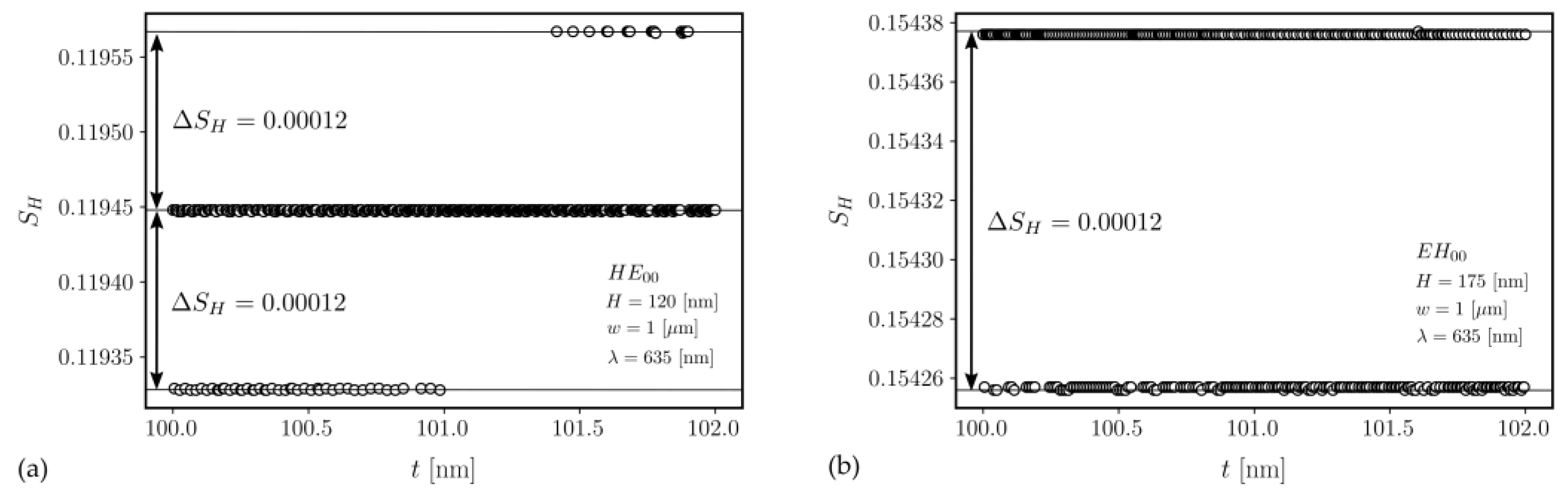
| H [nm] | t [nm] | w [μm] | SH | |
|---|---|---|---|---|
| HE00 | 120.0 | 100.0 | 1.0 | 0.1194 |
| EH00 | 175.0 | 100.0 | 1.0 | 0.1543 |
Disclaimer/Publisher’s Note: The statements, opinions and data contained in all publications are solely those of the individual author(s) and contributor(s) and not of MDPI and/or the editor(s). MDPI and/or the editor(s) disclaim responsibility for any injury to people or property resulting from any ideas, methods, instructions or products referred to in the content. |
© 2023 by the authors. Licensee MDPI, Basel, Switzerland. This article is an open access article distributed under the terms and conditions of the Creative Commons Attribution (CC BY) license (https://creativecommons.org/licenses/by/4.0/).
Share and Cite
Tyszkiewicz, C.; Kielan, P. Evanescent Wave Sensitivity of Silica-Titania Rib Waveguides in the Single-Mode Propagation Regime. Photonics 2023, 10, 1065. https://doi.org/10.3390/photonics10091065
Tyszkiewicz C, Kielan P. Evanescent Wave Sensitivity of Silica-Titania Rib Waveguides in the Single-Mode Propagation Regime. Photonics. 2023; 10(9):1065. https://doi.org/10.3390/photonics10091065
Chicago/Turabian StyleTyszkiewicz, Cuma, and Paweł Kielan. 2023. "Evanescent Wave Sensitivity of Silica-Titania Rib Waveguides in the Single-Mode Propagation Regime" Photonics 10, no. 9: 1065. https://doi.org/10.3390/photonics10091065