Article

Electrical Relaxation and Transport Properties of ZnGeP2 and 4H-SiC Crystals Measured with Terahertz Spectroscopy

by
Vladimir I. Voevodin
1,2,
Valentin N. Brudnyi
3,
Yury S. Sarkisov
4,
Xinyang Su
5 and
Sergey Yu. Sarkisov
1,6,*
1
Synchrotron Radiation Detector Laboratory, R&D Center “Advanced Electronic Technologies”, Tomsk State University, Tomsk 634050, Russia
2
LLC Laboratory of Optical Crystals, Tomsk 634040, Russia
3
Department of Semiconductor Physics, Tomsk State University, Tomsk 634050, Russia
4
Department of Physics, Chemistry and Theoretical Mechanics, Tomsk State University of Architecture and Building, Tomsk 634003, Russia
5
School of Physical Science and Engineering, Beijing Jiaotong University, Beijing 100044, China
6
Laboratory for Terahertz Research, Tomsk State University, Tomsk 634050, Russia
*
Author to whom correspondence should be addressed.
Photonics 2023, 10(7), 827; https://doi.org/10.3390/photonics10070827
Submission received: 21 June 2023 / Revised: 10 July 2023 / Accepted: 10 July 2023 / Published: 16 July 2023
(This article belongs to the Special Issue Ultrafast Optics and Applications)

Abstract

:
Terahertz photoconductivity and charge carrier recombination dynamics at two-photon (ZnGeP2) and three-photon (4H-SiC) excitation were studied. Thermally annealed, high-energy electron-irradiated and Sc-doped ZnGeP2 crystals were tested. The terahertz charge carrier mobilities were extracted from both the differential terahertz transmission at a specified photoexcitation condition and the Drude–Smith fitting of the photoconductivity spectra. The determined terahertz charge carrier mobility values are ~453 cm2/V·s for 4H-SiC and ~37 cm2/V·s for ZnGeP2 crystals. The charge carrier lifetimes and the contributions from various recombination mechanisms were determined at different injection levels using the model, which takes into account the influence of bulk and surface Shockley–Read–Hall (SRH) recombination, interband radiative transitions and interband and trap-assisted Auger recombination. It was found that ZnGeP2 possesses short charge carrier lifetimes (a~0.01 ps−1, b~6 × 10⁻¹⁹ cm3·ps−1 and c~7 × 10−40 cm6·ps−1) compared with 4H-SiC (a~0.001 ps−1, b~3 × 10⁻¹⁸ cm3·ps−1 and c~2 × 10−36 cm6·ps−1), i.e., τ~100 ps and τ~1 ns at the limit of relatively low injection, when the contribution from Auger and interband radiative recombination is small. The thermal annealing of as-grown ZnGeP2 crystals and the electron irradiation reduced the charge carrier lifetime, while their doping with 0.01 mass % of Sc increased the charger carrier lifetime and reduced mobility. It was found that the dark terahertz complex conductivity of the measured crystals is not fitted by the Drude–Smith model with reasonable parameters, while their terahertz photoconductivity can be fitted with acceptable accuracy.

1. Introduction

The optical pump–terahertz probe technique (OPTP) is a commonly adopted tool for the study of ultrafast carrier dynamics [1]. It has perfect temporal resolution and does not require any electrical contacts. On the other hand, a high level of photoexcitation is required to obtain measurable signals. Also, above-band-gap photoexcitation is usually employed, which makes the photoexcited area thin and can cause a dominant contribution from the surface states of a semiconductor. Thus, for a study of the pure bulk properties of a crystal, below-band-gap excitation (two- (TPA) or three-photon (3PA) absorption) is prospective [2]. In the present study, we investigated two wide-band-gap semiconductors, namely ZnGeP2 (Eg = 2 eV at 300 K) and 4H-SiC (Eg = 3.23 eV at 300 K), using photoexcitation with λ = 800 nm (the photon energy is 1.55 eV) femtosecond laser pulses. Thus, TPA works in the first case and 3PA in the second case.
ZnGeP2 crystals with a chalcopyrite structure have found their main application in IR nonlinear optics, while their properties for photovoltaic [3] and spintronics [4,5] applications have also been studied. It should be pointed out that while the linear and nonlinear optical properties of ZnGeP2 within the IR range are well studied, its electrical properties could be a subject of contradiction and were basically measured several decades ago [6,7]. ZnGeP2 growth technology has been considerably improved since that time and the electrical properties can be clearly affected by crystal perfectness and the presence of impurities. It is known that ZnGeP2 always has a p-type conductivity because of the charge neutrality level position in the lower part of the forbidden gap [8]. The published values for the mobility of holes are 0.1–60 cm2/V·s [6,7] while there are few data for the minority charge carrier mobility. In Ref. [6], the electron mobility was measured to be 103–104 cm2/V·s using the transit time technique. The dark terahertz conductivity employing terahertz time-domain spectroscopy (THz-TDS) was studied in Ref. [9]. The complex conductivity spectra were successfully fitted using the Drude–Smith model, but the reported carrier concentration and the static conductivity are several orders of magnitude higher than could be expected for undoped high-resistivity ZnGeP2. Recently, ultrafast optical pump–optical probe spectroscopy (the transient reflection measurement) was applied to ZnGeP2 crystals, and a charge carrier lifetime of 294 ps was deduced [10].
The ZnGeP2 crystals grown using state-of-the-art technology still have an “anomalous” absorption in the wavelength range of 0.62–3 μm, with an absorption maximum at the wavelength λ = 1 μm [11,12,13]. This absorption is associated with the optically active point defects [8]. Singly ionized zinc and phosphorus vacancies can act as such defects [8,10,13,14], as well as the GeZn antisite defect [10]. It is known that after thermal annealing or irradiation with high-energy electrons, the “anomalous” absorption in ZnGeP2 crystals is reduced [14,15]. The electron irradiation induces the formation of defects, resulting in the recharging of the acceptor levels and a decrease in their optical activity [8], while the Fermi level moves to the local electroneutrality level (about Ev + 0.8 eV). In Ref. [14], it is supposed that irradiation leads to the motion of interstitial atoms and the formation of Frenkel complexes with acceptor defects. In our previous study [11], we measured the absorption level for Sc-doped, annealed and electron-irradiated ZnGeP2 crystals (α = 7.3–21 cm−1 at λ = 800 nm). Thus, at below-band-gap excitation, the single-photon absorption (SPA) mechanism must also be taken into account at a moderate laser intensity used for photoexcitation.
The main application of ZnGeP2 crystals is mid-IR generation. The generation and detection of terahertz radiation is another potential application of ZnGeP2 crystals [11,16], but currently these crystals are scarcely used in the terahertz range, for example, in THz-TDS setups. Also, the doping of ZnGeP2 crystals to improve their properties for optical or photovoltaic applications has not been studied intensively. There have only been studies of ZnGeP2 doping with transition metals for spintronics [4,5]. All the above-mentioned points make the study of the terahertz properties of as-grown ZnGeP2 crystals modified by annealing, doping or electron irradiation relevant.
Silicon carbide has applications in high-field electronics. 4H-SiC possesses the broadest band gap among SiC polytypes. Because of its high radiation hardness together with its relatively high electron mobility (on the order of ~1000 cm2/V·s [17]) and long charge carrier lifetime, it is also prospective for ionizing radiation and high-energy particle detectors [18]. Both the charge carrier mobility and lifetime can decrease at high injection levels, which can occur in high-intensity fluxes. Thus, reliable contactless methods of controlling charge carrier mobility and lifetime at different injection levels are topical. The OPTP technique provides these possibilities. In our previous study, this technique was used to investigate another material for ionizing radiation and high-energy particle detectors, namely HR GaAs:Cr [19]. Previously, the OPTP technique with above-band-gap photoexcitation was applied to study 6H-SiC [20].
In the present study, we measured the terahertz photoconductivity and charge carrier recombination dynamics at below-band-gap SPA+TPA (ZnGeP2) and 3PA (4H-SiC) excitation. Thermally annealed, high-energy electron-irradiated and Sc-doped ZnGeP2 crystals were tested. The terahertz charge carrier mobilities were extracted from both differential terahertz transmission at a specified photoexcitation condition and the Drude–Smith fitting of the photoconductivity spectra.

2. Experimental Methods

2.1. Sample Preparation

The ZnGeP2 crystals were grown using the vertical Bridgman method [21]. In the first growth experiment (Exp. No. 1), the ZnGeP2 crystals were grown from high-purity initial components (Zn, Ge and P of 6N grade). Slabs of ZnGeP2 (Exp. No. 1) with thicknesses of ~0.2, 2 and 6.3 mm were prepared by cutting and polishing. The thermal annealing of the slabs (2 mm thick) was carried out in sealed ampoules with the addition of ZnGeP2 powder to create a vapor phase pressure in the ampule which prevented the decomposition of the material. The annealings were carried out at temperatures of 575–700 °C for 300–400 h [15]. The samples with thicknesses of 0.2 and 6.3 mm were irradiated with high-energy electrons (4 MeV) with a dose of ~2 × 1017 cm−2.
In the second growth experiment (Exp. No. 2), for the synthesis, Zn, Ge and P of 5N grade were used. The synthesized material was divided into two parts. To one part (50% of mass of synthesized material), scandium was added in an amount of 0.01 mass % of the total charge. Then, two ingots were crystallized using the same setup and growth conditions [11]. The slabs with thicknesses of about 200 μm were prepared from pure and scandium-doped ZnGeP2 (Exp. No. 2). All the slabs of ZnGeP2 had (001) orientation.
The studied semi-insulating (0001) 4H-SiC wafer had a thickness of 376 μm.

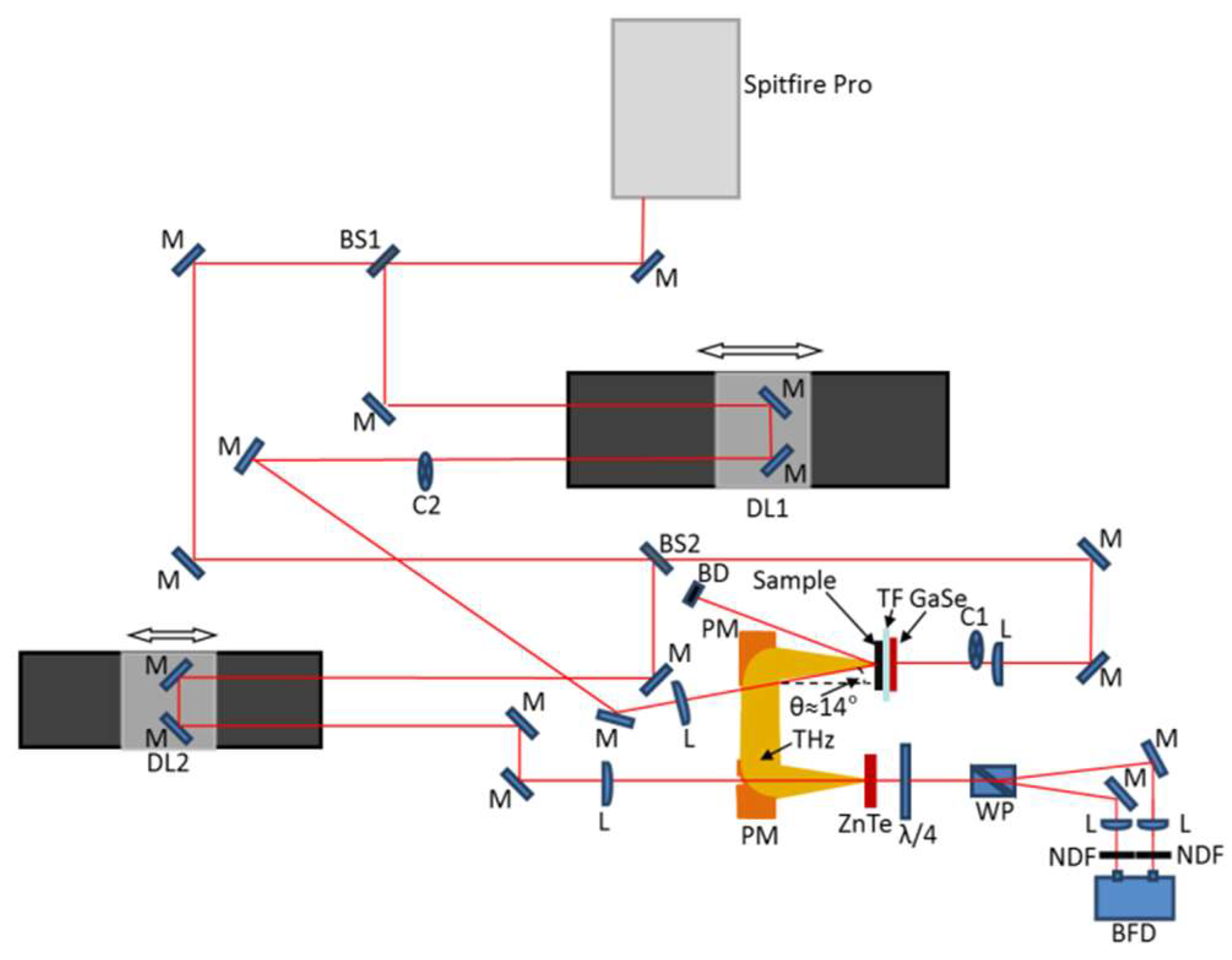
2.2. Optical Pump–Terahertz Probe Measurements

The charge carrier relaxation dynamics using the OPTP method and the terahertz photoconductivity were measured using the setup that is shown in Figure 1. As is known, the OPTP method is based on the probing of the changes in the terahertz transmittance or reflection of a sample by sending a terahertz pulse onto the sample with various time delays in reference to the short optical pulse, which induces the photogeneration of the free charge carriers [1]. The probing possibility is due to the absorption of terahertz radiation by free charge carriers.
For the sample photoexcitation, as well as for the generation and detection of the terahertz pulses, Spitfire Pro XP regenerative amplifier (Spectra-Physics, Milpitas, CA, USA), which generated pulses with a duration of 35 fs and energy up to 3.5 mJ at the central wavelength of 800 nm, was used (Figure 1). The laser pulse from the source, passing through the beam splitting plate (BS1) was divided into two pulses of approximately equal power. One of them, passing the delay line DL1, was used for the sample photoexcitation. The angle of incidence of the photoexcitation pulse θ was about 14° (i.e., the angle between the wavevector and the c-axis was about 4° inside the ZnGeP2 and about 5° inside the 4H-SiC crystal), and it had vertical polarization (i.e., pure ordinary wave). The angle θ was chosen to be as small as possible while preventing the reflected beam from hitting the aperture of the parabolic mirror and propagating to the detector. The second pulse was divided using another beam splitter (BS2). The more intense pulse (97% of power) extracted at BS2 passed through an SR-541 chopper (Standford Research, Sunnyvale, CA, USA) and was focused onto a GaSe crystal to generate a terahertz pulse via optical rectification [22,23]. Another pulse (3% of power) was directed to the delay line DL2 and then to a ZnTe electro-optical crystal for terahertz pulse detection. With the help of DL2, the simultaneity of the arrival to the ZnTe crystal of the probing optical pulse and the maximum terahertz pulse field strength (the main maximum) transmitted through the sample was established. The signal from the balanced photodetector (BPD) Nirvana Model 2007 (New Focus, Milpitas, CA, USA) was registered using a lock-in amplifier SR-830 (Standford Research, Sunnyvale, CA, USA). The length of the DL1 delay line allowed for obtaining a maximum delay of about 4 ns. The 1D terahertz transmittance scans were made (with DL1), i.e., the temporal profiles of the terahertz pulses were not recorded in the OPTP experiment and only changes in the terahertz pulse field strength at the main maximum were registered.
We measured the OPTP data for 4H-SiC and ZnGeP2 crystals under 3PA and combined SPA+TPA photoexcitation, respectively. In contrast to the commonly used above-band-gap SPA photoexcitation, in this case, the entire depth of a sample was photoexcited. Assuming 100% quantum efficiency, we calculated the concentration of generated electron–hole pairs on the distance x from the surface of a sample as
Δ n e - h _ p a i r s ( x ) = d I a b s ( x ) d x τ p η E p h o t
where Iabs(x) is the absorbed optical pump intensity after passing the thickness x of the crystal, τp is the pulse width, Ephot = hc/λ is the photon energy (c is the speed of light and λ is the laser wavelength) and η is the number of photons required to produce one electron–hole pair (η = 2 for SPA + TPA photoexcitation of ZnGeP2 and η = 3 for 3PA photoexcitation of 4H-SiC). The Iabs(x) for 3PA in 4H-SiC was calculated as
I a b s _ S i C ( x ) = I 0 1 1 ( 1 + 2 γ S i C x I 0 2 ) 0.5
where I0 = (1 − RSiC)P/S is the optical pump intensity passed through the entrance surface, P = Epumpp is the optical pump pulse peak power and Epump is the optical pump pulse energy, S is the optical pump spot area on the sample surface, RSiC = (nSiC − 1)2/(nSiC + 1)2 is the power reflection coefficient, where the refractive index nSiC(λ = 800 nm) = 2.6 [24] and γSiC is the 3PA coefficient (γSiC =2.5 × 10⁻²² cm3/W2 for 4H-SiC at λ = 800 nm [25]). Here, we neglect the angular dependence of the reflection coefficient for simplicity. The difference in the reflection coefficient for exactly normal incidence and for incidence at the angle θ = 14° is small (below 5% for both ZnGeP2 and 4H-SiC crystals).
For ZnGeP2, the Iabs(x) was calculated as
I a b s _ Z G P ( x ) = I 0 I ( x )
Here, the optical pump intensity reaching the depth x inside the crystal I(x) was calculated by numerically solving the equation
d I ( x ) d x = I ( x ) ( α Z G P + β Z G P I ( x ) )
where the SPA coefficient αZGP is 7.3–21 cm−1 [11] (see Table 1), the TPA coefficient βZGP = 11.3 × 10⁻⁹ cm/W was taken from [26] for λ = 800 nm, I0 = (1 − RZGP)P/S and nZGP(λ = 800 nm) = 3.34 [27]. When calculating the absorbed power (2)–(4), we neglected the possible multiple reflections.
The concentration of electron–hole pairs Δne-h_pairs(x) was calculated employing relation (1) with the Iabs(x) calculated from Equations (2) or (3) and (4). The average concentration of electron–hole pairs over crystal length L was calculated as
Δ n ( L ) = I a b s ( L ) L τ p η E p h o t
For the relatively thick (L = 2 mm) ZnGeP2 samples, treated via annealing and electron irradiation, taking into account the large ZnGeP2 TPA coefficient, it would be required to apply a photoexcitation laser pulse peak intensity as low as 0.45 GW/cm2 to obtain uniform distribution of the generated charge carriers (the difference in Δne-h_pairs(x) on the front and opposite surfaces within an order of magnitude) with the average electron–hole pair concentration Δn(L = 2 mm) on the order of 1.3 × 1014 cm−3. Such an initial concentration of the photogenerated charge carriers together with the low charge carrier mobility in ZnGeP2 would not allow for recording a complete OPTP scan because of the low signal. Thus, to measure these samples we increased the I0 to 40 GW/cm2 (the laser pulse average power Pav = 250 mW at the beam spot diameter d = 4 mm) to obtain the sharper Δne-h_pairs(x) distribution. It should be pointed out that at this intensity and at the used laser pulse repetition rate of 1 kHz the crystals were not damaged, but obviously, the intensity could not be raised considerably to further increase the gradient of Δne-h_pairs(x) without damage to the crystals. The laser spot diameter was measured employing an optical microscope. It should be mentioned that the samples were not thermally stabilized in our experiments. Therefore, local heating of the samples under the photoexcitation pulse occurred. In our previous study [19], we measured the temperature of GaAs slabs under similar photoexcitation conditions employing a thermocouple, and the measured surface temperature did not exceed the room temperature by more than 50 °C. The increased temperature definitely influences the charge carrier concentration, the scattering and recombination rates. For example, the SRH recombination rate is proportional to the thermal velocity of holes and electrons (see, for example, Supplementary Materials to Ref. [19]). The thermal velocities scale as square root of the temperature. Thus, heating from 300 to 350 °C increases the scattering rate and reduces the charge carrier lifetime by ~8% due to this factor. In further analysis, we neglected the local heating, assuming that it does not significantly change the parameters typical for the room temperature. This is also confirmed by the results of [9], where the deduced scattering time and charge carrier concentration for the temperatures of 250 and 300 °C were quite close to each other.
Usually, for a thin photoconducting layer with a thickness δ << λTHz and δ << L, to calculate the nonequilibrium charge carrier concentration using the measured differential transmission ΔT/T0 values, the following formula is used [1]:
Δ n ( t ) = n T H Z + 1 Z 0 e δ μ ( 1 1 Δ T ( t ) T 0 1 )
where nTHz is the terahertz refractive index of the slab, Z0 = 377 Ω is the free space impedance, e is the electron charge, μ is the carrier mobility (sum of electron μn and μh hole mobilities) averaged over all the measured terahertz frequencies, ΔT(t) = T(t) – T0, where T(t) and T0 are the sample terahertz amplitude transmittances with and without photoexcitation and t is the delay between the arrival of the laser pump and terahertz probe pulses to the sample surface. The possible charge carrier mobility dependence on the injection level is neglected here.
At the photoexcitation laser pulse peak intensity specified above, Δne-h_pairs(x) drops by one order of magnitude at distance x from the surface of 47 μm, from 1.3 × 1018 cm−3 at the very surface to 1.3 × 1017 cm−3 (Figure 2a), and to 1.3 × 1014 cm−3 at the opposite face of a 2 mm thick sample. The value of Δn averaged over distance from the surface from x = 0 to x = 47 μm is 4.2 × 1017 cm−3. Thus, the use of Equation (6) here is a somewhat rough approximation, but it can be justified partly by the fact that the conductivity within the layer of thickness 47 μm is more than one order of magnitude higher than in the rest of the slab and the thickness of this layer is more than one order of magnitude less than the slab thickness. On the other hand, its thickness, while being large enough for a “bulk semiconductor”, is only 4 times less than the shortest detectable in our experiment’s terahertz wavelength (ν = 1.5 THz, λTHz = 150 μm). This is partly adjusted by the maximum spectral sensitivity of the used terahertz emitter, which was about ν = 0.65 THz, i.e., λTHz = 461 μm. In Figure 2a, it is seen that at the high photoexcitation laser pulse peak intensity in ZnGeP2, the total absorption and the charge carrier generation are dominated by TPA (the SPA+TPA and TPA curves are merged in Figure 2a).
In the case of 200 μm thick ZnGeP2 samples and 376 μm thick 4H-SiC wafers, a more uniform distribution of Δne-h_pairs(x) could be obtained. For a uniform charge carrier distribution, to calculate the nonequilibrium charge carrier concentration by using the obtained relative differential transmission ΔT/T0 values, the following formula was employed [2]:
Δ n ( t ) = 2 n T H z Z 0 e L μ Δ T ( t ) T 0
In the case of 4H-SiC, the presence of the thin high-quality wafer and the combination of a high enough charge carrier mobility and a low enough value of 3PA coefficient provided the possibility to obtain a high terahertz probe sensitivity at close to uniform nonequilibrium charge carrier density distribution at Pav = 140 mW and beam spot diameter d = 3 mm (Figure 2b and Table 1). Both the terahertz photoconductivity and OPTP data in 4H-SiC were measured at these excitation conditions. To obtain a measurable signal, the pump beam had to be focused to d = 3 mm spot.
For ZnGeP2, the situation is less convenient, as it possesses a high TPA coefficient and also a high level of SPA at λ = 800 nm (Table 1). Also, it is difficult to obtain high-quality slabs of ZnGeP2 with polished surfaces with L < 200 μm. Taking into account the low carrier mobility of ZnGeP2, there is a trade-off between sensitivity of measurements and uniformity of charge carrier density distribution. For the measurements of the 200 μm thick samples, Pav = 150 mW and the beam spot diameter d = 6 mm were used, giving I0 of about 11 GW/cm2. At these excitation parameters, there is an observable difference between the SPA+TPA and pure TPA-generated e-h pair concentrations (Figure 2b). The e-h pair concentrations on the front and the opposite surfaces of the sample differ by a little more than one order of magnitude, which we consider to be a uniform distribution; we used the values of Δn averaged over distance from the surface from x = 0 to x = L in the further calculations (Table 1). It should be pointed out that the high excitation limit is applicable to our measurements as Δn >> ni, n0, p0 for both 4H-SiC and ZnGeP2 samples.
Knowing the Δn(t = 0) (Table 1) and measured ΔT(t = 0)/T0 values, the averaged charge carrier mobilities μ = μn + μp over all measured terahertz frequencies were estimated using Equations (6) and (7).
In order to account for the charge carrier lifetime dependence on the injection level and to distinguish the contributions from the different recombination mechanisms, the following equation was used [28]:
1 Δ n ( t ) d Δ n ( t ) d t = 1 τ eff = a + b Δ n ( t ) + c Δ n 2 ( t )
where τeff is the effective charge carrier lifetime, the a coefficient is responsible for the influence of surface and bulk SRH recombination, the b coefficient is associated with the effect of interband radiative transitions and Auger recombination through trap levels and the c coefficient is responsible for the interband Auger recombination effect. The solution of Equation (8), assuming that b2 > 4ac and after swapping the dependent and independent variables, is
t = k 1 2 a ln Δ n 2 a + b Δ n + c Δ n 2 + b 2 a b 2 4 a c ln b + 2 c Δ n b 2 4 a c b + 2 c Δ n + b 2 4 a c
while for b2 < 4ac the solution is
t = k 1 2 a ln Δ n 2 a + b Δ n + c Δ n 2 + b a 4 a c b 2 arctan b + 2 c Δ n 4 a c b 2
The experimental dependences Δn(t) were plotted in t-Δn coordinates and fitted by Equation (9) as it better fitted the obtained experimental data compared with Equation (10).

2.3. Terahertz Photoconductivity Measurements

In order to measure the terahertz dielectric constants and conductivities of photoexcited samples, the same setup was employed (Figure 1). Basically, in these measurements, the delay line DL1 was fixed at two positions. At the first position (Δt1 = 0), the minimum of the terahertz transmission, i.e., simultaneous arrival of the maximal amplitude of the terahertz waveform and the pump pulse to the sample, was provided. The second position (Δt2) was chosen to obtain −ΔT(t)/T0 values two times lower than at the first position. At these two fixed positions of DL1, the delay line DL2 was scanned to obtain the terahertz waveforms. As DL1 was fixed during this scan, the different parts of terahertz waveforms passing the sample basically experienced different photoexcitation levels. To minimize this effect, the maximum delay provided by DL2 was chosen to be as short as 15 ps. To obtain the dark photoconductivity spectra, the DL2 scan was recorded with the blocked pump pulse.
In the next step, the standard THz-TDS data analysis [1] was performed to obtain ε’(ω) and ε’’(ω). Knowing the complex dielectric constants, the terahertz refractive indices and the absorption coefficients were calculated using the following well-known formulas:
n T H z ( ω ) = 1 2 ε 2 ( ω ) + ε 2 ( ω ) + ε ( ω ) 0.5
α ( ω ) = 2 ω c 1 2 ε 2 ( ω ) + ε 2 ( ω ) ε ( ω ) 0.5
The dark complex conductivities (of free electrons) were calculated, assuming the dominant contribution to the dielectric function from the core electrons and the free carriers, as
σ d a r k ( ω ) = ω ε d a r k ( ω ) ε 0
σ d a r k ( ω ) = ω ε 0 ( ε ε d a r k ( ω ) )
Here, the high-frequency dielectric constant for 4H-SiC (ε = 6.52) was taken from [29] and that for ZnGeP2 = 10.04) from [30].
The photoexcited carrier-induced complex conductivities were calculated as
Δ σ ( ω ) = ω ε 0 ( ε p h o t ( ω ) ε d a r k ( ω ) )
Δ σ ( ω ) = ω ε 0 ( ε d a r k ( ω ) ε p h o t ( ω ) )
The terahertz complex dielectric constants measured with (ε′phot(ω) and ε″phot(ω)) and without (ε′dark(ω) and ε″dark(ω)) photoexcitation of a sample were substituted into (13)–(16).
The experimental terahertz complex conductivities were approximated with the widely used Drude–Smith formula:
Δ σ ( ω ) = Δ n e 2 τ m * ( 1 i ω τ ) 1 + c b 1 i ω τ
where τ is the momentum relaxation time, m* is the charge carrier effective mass and cb is the parameter of backscattering [1]. The charge carrier mobilities were also estimated using the obtained τ values as μ = τe/m*. The values m* = 0.108me for ZnGeP2 [9] and m* = 0.42me for 4H-SiC [31] were used, where me is the free electron mass. If both electrons and holes give comparable contributions to conductivity, the total conductivity expression must be composed of two Drude-Smith terms (Equation (17)) written for electrons and holes, respectively. Usually, the contribution from minority or lower mobility carriers is neglected.

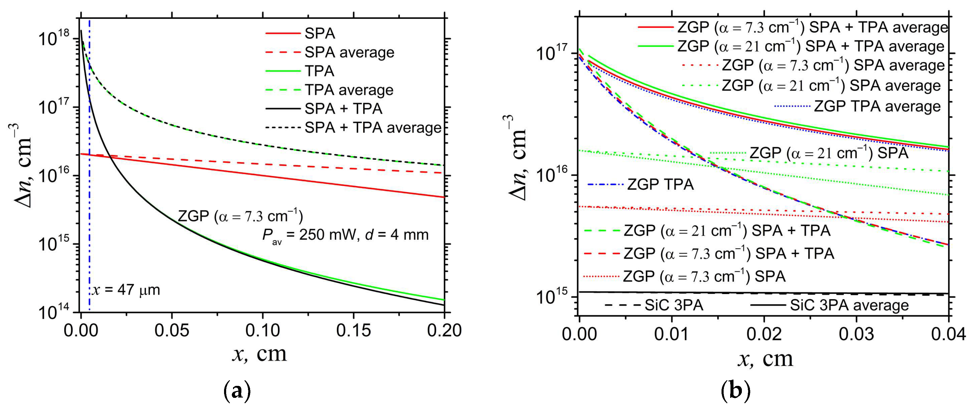
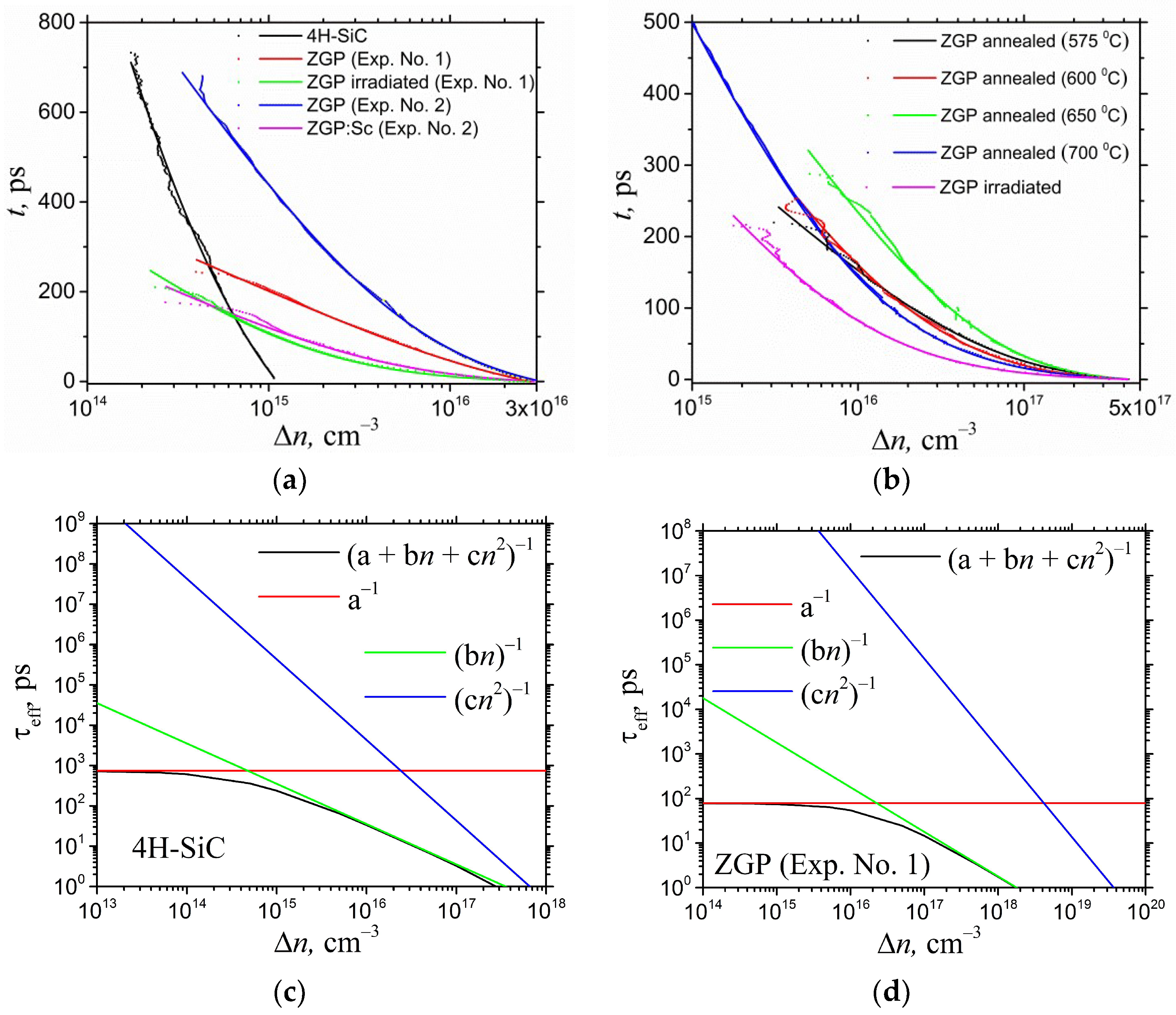
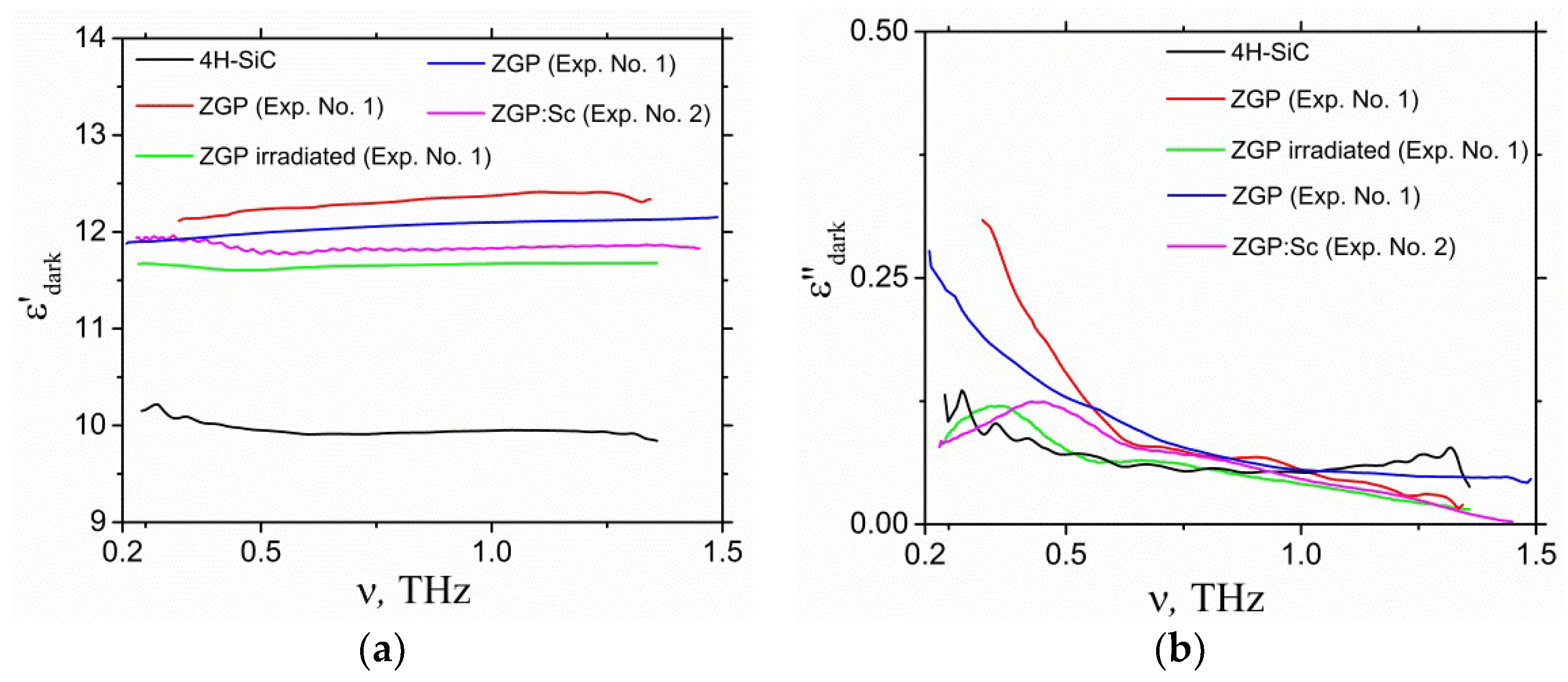
3. Results and Discussion

The obtained temporal profiles of the nonequilibrium charge carrier concentration for the thin samples are shown in Figure 3a. It can be directly seen that 4H-SiC possesses longer charge carrier lifetimes compared with the ZnGeP2 samples. This is due to the natural properties of the materials, including the larger band gap of 4H-SiC, which reduces the probability of the capture of the charge carriers to recombination centers with energy levels near the midgap. Also, ZnGeP2 crystals contain more defects acting as efficient recombination centers. This is predicted by the thermodynamic properties of these two systems and also by the fact that the growth technology of SiC is more advanced, since this material is required for microelectronics. The charge carrier lifetime in ZnGeP2 (Exp. No. 2) is clearly longer than in the other ZnGeP2 samples. The doping of ZnGeP2 (Exp. No. 2) with scandium results in a decrease in the lifetime. This can be explained by the generation of recombination centers or by the recharging of traps. Electron irradiation slightly increases the charge carrier lifetime in ZnGeP2 (Exp. No. 1). This in turn could be attributed to the generation of traps or to a reduction in the concentration of active recombination centers.
It could be supposed that the defects with energy levels close to the midgap can act as recombination centers (probably P vacancies in different charge states in ZnGeP2 [8,10]). On the contrary, the defects with energy levels close to the energy bands act as traps for the charge carriers (Ge and Zn vacancies, as well as the GeZn antisite defect [8,10]). It is believed that electron irradiation generates point defects, first of all vacancies of P, Zn and Ge, while the interstitial atoms are easily annealed and clustered [8]. The generation of these defects moves the Fermi level upwards to the midgap and reduces the number of neutral acceptors which are responsible for “anomalous” absorption [8] (and the opposite process, recombination). Thus, the recharging of the recombination centers reduces their efficiency (changes their occupancy and energy position), and the a coefficient in (8) decreases. Doping with Sc also reduces the “anomalous” absorption, and it could be supposed that scandium-related defects (interstitial atoms or antisites) form a donor level in the upper half of the band gap. This also results in a Fermi level shift upwards, but the Sc-related defects themselves may act as a trap for the charge carriers, increasing their lifetime. Interestingly, the b coefficient, on the contrary, increases (decreases) after the electron irradiation (Sc doping) of ZnGeP2 crystals. This may be due to the competitive character of radiative band-to-band and SRH recombination. The b coefficient also includes a contribution from trap-assisted Auger recombination. Thus, the decrease in the b coefficient (while the a coefficient increases) may demonstrate that the Auger and SRH recombination passes through different defect states. For a more robust analysis, additional experiments, including photoluminescence measurements and electron microscopy, are required.
The measured OPTP data for thick samples of ZnGeP2 annealed at various temperatures and irradiated using high-energy electrons are presented in Figure 3b. Here, it can be observed that at a low level of injection (when the SRH recombination is dominant), the charge carrier lifetime increases with the increasing temperature of the annealing (see also parameter a in Table 2). It is observed that the a parameters determined from OPTP data measured at different photoexcitation laser pulse intensities in the slabs of the same material (irradiated ZnGeP2 (Exp. No. 1)) but having different thicknesses (L = 200 μm and L = 6.3 mm) almost do not differ. On the other hand, the differences in the b and c parameters are considerable (order of magnitude).
The measured values of ΔT(t = 0)/T0 and the corresponding calculated values of μ (from relations (6) and (7)) are given in Table 2. The fitting parameters a, b and c from Formula (9) are also provided (Table 2). It should be pointed out that the parameter a values are the most reliable and well reproduced. For obtaining more reliable values of the c parameter the measurements at higher levels of excitation, when the contribution from interband Auger recombination would be significant (about 1020 cm−3 for ZnGeP2 and 1018 cm−3 for 4H-SiC crystals, Figure 3c,d), are required. In Figure 3c,d, the black curves represent the dependence τeffn) according to Equation (9) for the 4H-SiC and ZnGeP2 (Exp. No. 1) samples, respectively. The red curves represent the lifetime if it was determined only by the surface and bulk SRH recombination (the values b = c = 0 were substituted into Equation (8)). Similarly, the green and blue curves describe the contributions of radiative recombination together with Auger recombination via traps (at a = c = 0 substituted into (8)) and interband Auger recombination (at a = b = 0 substituted into (8)). The analogous plots for the rest of the samples are presented in the Supplementary Materials (Figures S1–S4).
The complex terahertz photoconductivity spectra (expected to be determined dominantly by the free carrier contribution) measured at the two different photoexcitation levels are shown in Figure 4. It can be seen that the values of the real parts of the conductivity measured at Δt1 (Figure 4a) and Δt2 (Figure 4c) differ by about two times, in accordance with the photoexcitation level for all the samples. The highest terahertz photoconductivity is observed in ZnGeP2 (Exp. No. 1). For ZnGeP2 (Exp. No. 2) and ZnGeP2 (Exp. No. 1), the photoconductivity decreased after Sc doping and electron irradiation, respectively. The Drude–Smith model better reproduces data for the 4H-SiC sample, but still approximately reproduces the terahertz photoconductivity spectra of the ZnGeP2 samples as well (the fitting parameters are given in Table 3). It should be pointed out that the Drude–Smith model did not allow fitting the experimental data for dark terahertz photoconductivity for our high-resistivity samples with realistic parameters. This could be in accordance with the results of [32,33], where the dominant contribution of combined two-phonon processes (exceeding the Drude-like free-carrier contribution by more than an order of magnitude) to the terahertz dielectric constant in ZnGeP2 was deduced. The measured dark terahertz dielectric constants are presented in Figure 5. The related spectra of the absorption coefficient and the refractive indices calculated using relations (11) and (12) are given in the Supplementary Materials (Figure S5).
In the Supplementary Materials (Figure S6 and Table S1), we also provide the results of our attempt to fit the dark terahertz complex conductivities calculated using relations (13) and (14) with the Drude–Smith formula (17).
It was found that doping with Sc reduces the terahertz charge carrier mobility. The low-frequency charge carrier mobility in ZnGeP2 also decreases at doping [7] (by two orders of magnitude at doping with In). The electrical parameters of the undoped ZnGeP2 reported in [7], a hole concentration on the order of 1010 cm−3 and conductivity on the order of 2 × 10⁻⁵ Ohm−1cm−1 are close to the parameters of the crystals tested in the present study. In a recent study [9], the dark terahertz conductivity of ZnGeP2 was studied, employing THz-TDS and the Drude–Smith model. The complex conductivity spectra were successfully fitted using the Drude–Smith model, but the reported parameters for carrier concentration on the order of ~6.4 × 1016 cm−3 and the level of static conductivity ~0.175 Ohm−1cm−1 are several orders of magnitude higher than could be expected for undoped high-resistivity ZnGeP2. The level of room temperature terahertz mobility on the order of ~150 cm2/V·s [9] is also higher than that measured in our experiments, except for the ZnGeP2 (Exp. No. 1) data following from the Drude–Smith fitting (Table 3). On the other hand, we believe that the charge carrier mobility values (Table 2) obtained from the OPTP data are more reliable for our experiments. This is explained by the fact that it is difficult to measure terahertz conductivity in semi-insulating samples with good precision because of their low absorption. The noisy character of the obtained dark conductivity spectra (Figure S6) demonstrates this. Also, it is known that accurate evaluation of the sample thickness and accounting for the multiple reflections in the setup, especially in the sample and the electro-optic detector crystal, are required to extract the undistorted spectra of the dielectric constants [1]. This can be done by choosing a proper time window and applying special algorithms for the THz-TDS data analysis The influence of these issues, as well as the standard problems of the presence of water absorption lines and pump laser noise, could be the reason for some modulations on the curves plotted in Figure 4 and Figure 5 (and Figures S5 and S6 in the Supplementary Materials). The quality of the obtained Drude–Smith fitting (Figure 4) is not perfect, especially for the imaginary parts of the complex conductivity for the ZnGeP2 samples. The values of the charge carrier mobility in ZnGeP2 obtained in the present study are two orders of magnitude lower than the electron mobility values measured in Ref. [6].
The determined charge carrier mobility values for 4H-SiC (Table 2 and Table 3) agree well with the electron mobility value of about 1000 cm2/V·s reported in [17], but are lower than the 105 cm2/V·s value published in [31] for 4H-SiC. The latter value seems to be overestimated.

4. Conclusions

In conclusion, terahertz photoconductivity and charge carrier recombination dynamics at below-band-gap excitation in ZnGeP2 and 4H-SiC crystals were studied. Also, annealed, high-energy electron-irradiated and Sc-doped ZnGeP2 crystals were tested. The terahertz charge carrier mobilities were estimated both from the differential terahertz transmission at a specified photoexcitation condition and from the Drude–Smith fitting of the photoconductivity spectra. The determined charge carrier mobility values are ~453 cm2/V·s for 4H-SiC and ~37 cm2/V·s for ZnGeP2 crystals. The charge carrier lifetimes and the contributions from various recombination mechanisms, namely surface and volume SRH recombination, interband radiative transitions and interband and trap-assisted Auger recombination were determined at different injection levels. It was found that ZnGeP2 crystals possess shorter charge carrier lifetimes (a~0.01 ps−1, b~6 × 10⁻¹⁹ cm3·ps−1 and c = 7 × 10−40 cm6·ps−1) compared with 4H-SiC (a~0.001 ps−1, b~3 × 10⁻¹⁸ cm3·ps−1 and c~2 × 10−36 cm6·ps−1), i.e., τ = 100 ps and τ = 1 ns at the limit of relatively low injection, when the contribution from Auger and interband radiative recombination is small. It was found that the thermal annealing of as-grown ZnGeP2 crystals and electron irradiation reduce the charge carrier lifetime, while their doping with 0.01 mass % of Sc increases the charger carrier lifetime and reduces their mobility. The Auger recombination mechanisms make a decisive contribution to the recombination rate of nonequilibrium charge carriers at injection levels > 5 × 1015 cm−3 for ZnGeP2 and >5 × 1014 cm−3 for 4H-SiC. At lower carrier concentrations, the SRH recombination prevails.
It was found that the dark complex conductivity of the measured semi-insulating 4H-SiC and ZnGeP2 crystals is not fitted by the Drude–Smith model with reasonable parameters. After photoexcitation, the free carrier concentration increases by six orders of magnitude and the Drude-like contribution becomes dominant. In this case, the Drude–Smith model can reproduce the data with reasonable τ and Δn parameters.
The obtained results indicate the possibility of applying the OPTP technique for determining charge carrier lifetime and mobility in semiconductor crystals intended for the manufacturing of ionizing and high-energy particle detectors. These parameters determine the efficiency of such devices.

Supplementary Materials

The following supporting information can be downloaded at: https://www.mdpi.com/article/10.3390/photonics10070827/s1, Figure S1: Calculated injection level dependences of efficient charge carrier lifetime with the resolution into contributions from different recombination mechanisms for (a) ZnGeP2 (Exp. No. 2) and (b) ZnGeP2:Sc (Exp. No. 2); Figure S2: Calculated injection level dependences of efficient charge carrier lifetime with the resolution into contributions from different recombination mechanisms for (a) ZnGeP2 (Exp. No. 1) annealed at T = 575 °C and (b) ZnGeP2 (Exp. No. 1) annealed at T = 600 °C; Figure S3: Calculated injection level dependences of efficient charge carrier lifetime with the resolution into contributions from different recombination mechanisms for (a) ZnGeP2 (Exp. No. 1) annealed at T = 650 °C and (b) ZnGeP2 (Exp. No. 1) annealed at T = 700 °C; Figure S4: Calculated injection level dependences of efficient charge carrier lifetime with the resolution into contributions from different recombination mechanisms determined for (a) thin and (b) thick slab of electron irradiated ZnGeP2 (Exp. No. 1); Figure S5: The terahertz spectra of (a) refractive index and (b) absorption coefficient of ZnGeP2 (Exp. No. 1), electron irradiated ZnGeP2 (Exp. No. 1), ZnGeP2:Sc (Exp. No. 2), ZnGeP2:Sc (Exp. No. 2) and 4H-SiC crystals; Figure S6: The terahertz spectra of (a) real and (b) imaginary parts of dark complex conductivity measured in ZnGeP2 (Exp. No. 1), electron irradiated ZnGeP2 (Exp. No. 1), ZnGeP2:Sc (Exp. No. 2), ZnGeP2:Sc (Exp. No. 2) and 4H-SiC crystals. Symbols—experimental data, solid lines—Drude-Smith fitting (the parameters are given in Table S1); Table S1: The Drude-Smith model fitting parameters (for fitting of dark complex conductivity measured in ZnGeP2 (Exp. No. 1), electron irradiated ZnGeP2 (Exp. No. 1), ZnGeP2 (Exp. No. 2), ZnGeP2:Sc (Exp. No. 2) and 4H-SiC crystals).

Author Contributions

Conceptualization, V.N.B., Y.S.S. and S.Y.S.; methodology, V.I.V. and S.Y.S.; software, S.Y.S.; validation, V.N.B., X.S. and S.Y.S.; formal analysis, S.Y.S.; investigation, V.I.V., X.S. and S.Y.S.; resources, V.I.V. and V.N.B.; data curation, X.S. and S.Y.S.; writing—original draft preparation, S.Y.S..; writing—review and editing, X.S. and S.Y.S.; visualization, V.I.V.; supervision, S.Y.S.; project administration, S.Y.S.; funding acquisition, S.Y.S. All authors have read and agreed to the published version of the manuscript.

Funding

The part of the research focused on the study of ZnGeP2 crystals was funded by the Ministry of Science and Higher Education of the Russian Federation (project No. FSWM-2020-0038). The part of the research focused on the study of 4H-SiC crystals was funded by a grant under the Decree of the Government of the Russian Federation No. 220 of 09 April 2010 (Agreement No. 075-15-2022-1132 of 01 July 2022).

Institutional Review Board Statement

Not applicable.

Informed Consent Statement

Not applicable.

Data Availability Statement

The data presented in this study are available in the article and Supplementary materials.

Conflicts of Interest

The authors declare no conflict of interest.

References

  1. Jepsen, P.U.; Cooke, D.G.; Koch, M. Terahertz spectroscopy and imaging—Modern techniques and applications. Las. Phot. Rev. 2011, 5, 124–166. [Google Scholar] [CrossRef]
  2. Wahlstrand, J.K.; Heilweil, E.J. Contactless THz-based bulk semiconductor mobility measurements using two-photon excitation. Opt. Express 2018, 26, 29848–29853. [Google Scholar] [CrossRef]
  3. Rud’, V.Y.; Rud’, Y.V. ZnGeP2 heterocontact with layered III–VI semiconductors. Tech. Phys. Lett. 1997, 23, 415–416. [Google Scholar] [CrossRef]
  4. Bacewicz, R.; Pietnoczka, A.; Gehlhoff, W.; Voevodin, V.G. Local order in ZnGeP2:Mn crystals. Phys. Status Solidi A 2007, 204, 2296–2301. [Google Scholar] [CrossRef]
  5. Sarkisov, S.Y.; Picozzi, S. Transition-metals doping of semiconducting chalcopyrites: Half-metallicity and magnetism. J. Phys. Condens. Matter 2007, 19, 016210. [Google Scholar] [CrossRef]
  6. Ray, B.; Payne, A.J.; Burell, G.J. Preparation and some physical properties of ZnGeP2. Phys. Status Solidi 1969, 35, 197–204. [Google Scholar] [CrossRef]
  7. Grigoreva, V.S.; Prochukhan, V.D.; Rud, Y.V.; Yakovenko, A.A. Some electrical properties of high-resistance ZnGeP2 single crystals. Phys. Status Solidi 1973, 17, K69–K74. [Google Scholar] [CrossRef]
  8. Brudnyi, V.N.; Budnitskii, D.L.; Krivov, M.A.; Masagutova, R.V.; Prochukhan, V.D.; Rud, Y.V. The electrical and optical properties of 2.0 MeV electron-irradiated ZnGeP2. Phys. Status Solidi 1978, 50, 379–384. [Google Scholar] [CrossRef]
  9. Sooriyagoda, R.; Piyathilaka, H.P.; Zawilski, K.T.; Schunemann, P.G.; Bristow, A.D. Carrier transport and electron–lattice interactions of nonlinear optical crystals CdGeP2, ZnGeP2, and CdSiP2. J. Opt. Soc. Am. B 2021, 38, 769–775. [Google Scholar] [CrossRef]
  10. Pan, X.; Wang, Y.; Bai, H.; Ren, C.; Peng, J.; Jing, F.; Qiu, H.; Lei, Z.; Liu, H.; Yang, C.; et al. Atomic structures and carrier dynamics of defects in a ZnGeP2 crystal. Chin. Opt. Lett. 2023, 21, 041604. [Google Scholar] [CrossRef]
  11. Voevodin, V.I.; Bereznaya, S.A.; Sarkisov, Y.S.; Yudin, N.N.; Sarkisov, S.Y. Terahertz generation by optical rectification of 780 nm laser pulses in pure and Sc-doped ZnGeP2 crystals. Photonics 2022, 9, 863. [Google Scholar] [CrossRef]
  12. Yang, Y.; Zhang, Y.; Gu, Q.; Zhang, H.; Tao, X. Growth and annealing characterization of ZnGeP2 crystal. J. Cryst. Growth 2011, 318, 721–724. [Google Scholar] [CrossRef]
  13. Zawilski, K.T.; Schuneman, P.G.; Setzler, S.D.; Pollak, T.M. Large aperture single crystal ZnGeP2 for high-energy applications. J. Cryst. Growth 2008, 310, 1891–1896. [Google Scholar] [CrossRef]
  14. Lei, Z.; Zhu, C.; Xu, C.; Yao, B.; Yang, C. Growth of crack-free ZnGeP2 large single crystals for high-power mid-infrared OPO applications. J. Cryst. Growth 2014, 389, 23–29. [Google Scholar] [CrossRef]
  15. Gribenyukov, A.I.; Voevodin, V.I. Influence of the preparation conditions on optical properties of single crystals ZnGeP2 in THz range. J. Phys. Conf. Ser. 2018, 1115, 052030. [Google Scholar] [CrossRef] [Green Version]
  16. Li, F.; Zhong, K.; Qiao, H.; Liu, K.; Zhang, X.; Xu, D.; Yao, J. Efficient tunable terahertz generation via noncollinear phase matching in the ZnGeP2 crystal. J. Opt. Soc. Am. B 2020, 37, 3857–3864. [Google Scholar] [CrossRef]
  17. Pernot, J.; Contreras, S.; Camassel, J.; Robert, J.L.; Zawadzki, W.; Neyret, E.; Di Cioccio, L. Free electron density and mobility in high-quality 4H–SiC. Appl. Phys. Lett. 2000, 77, 4359–4361. [Google Scholar] [CrossRef]
  18. Strokan, N.B.; Ivanov, A.M.; Lebedev, A.A. SiC nuclear-radiation detectors. In SiC Power Materials. Springer Series in Materials Science; Feng, Z.C., Ed.; Springer: Berlin/Heidelberg, Germany, 2004; Volume 73. [Google Scholar] [CrossRef]
  19. Kolesnikova, I.A.; Kobtsev, D.A.; Redkin, R.A.; Voevodin, V.I.; Tyazhev, A.V.; Tolbanov, O.P.; Sarkisov, Y.S.; Sarkisov, S.Y.; Atuchin, V.V. Optical pump—THz probe study of HR GaAs:Cr and SI GaAs:EL2 structures with long charge carrier lifetimes. Photonics 2021, 8, 575. [Google Scholar] [CrossRef]
  20. Li, G.; Nie, X.; Liao, Y.; Yin, W.; Zhou, W.; Gao, Y.; Xia, N.; Cui, H. Photogenerated carrier density dependence of ultrafast carrier dynamics in intrinsic 6H-SiC measured by optical-pump terahertz-probe spectroscopy. Opt. Commun. 2022, 511, 127979. [Google Scholar] [CrossRef]
  21. Verozubova, G.A.; Gribenyukov, A.I.; Korotkova, V.V.; Ruzaikin, M.P. ZnGeP2 synthesis and growth from melt. Mater. Sci. Eng. B 1997, 48, 191–197. [Google Scholar] [CrossRef]
  22. Redkin, R.A.; Kobtsev, D.A.; Bereznaya, S.A.; Korotchenko, Z.V.; Sarkisov, Y.S.; Mihaylov, T.A.; Sarkisov, S.Y. GaSe crystals with antireflection coatings for terahertz generation. Mater. Res. Express 2019, 6, 126201. [Google Scholar] [CrossRef]
  23. Voevodin, V.I.; Yudin, N.N.; Sarkisov, S.Y. Influence of thermal annealing on terahertz dielectric properties of ZnGeP2 crystals. Russ. Phys. J. 2021, 64, 1513–1516. [Google Scholar] [CrossRef]
  24. Wang, S.; Zhan, M.; Wang, G.; Xuan, H.; Zhang, W.; Liu, C.; Xu, C.; Liu, Y.; Wei, Z.; Chen, X. 4H-SiC: A new nonlinear material for midinfrared lasers. Las. Phot. Rev. 2013, 7, 831–838. [Google Scholar] [CrossRef]
  25. Guo, X.; Peng, Z.; Ding, P.; Li, L.; Chen, X.; Wei, H.; Tong, Z.; Guo, L. Nonlinear optical properties of 6H-SiC and 4H-SiC in an extensive spectral range. Opt. Mater. Express 2021, 11, 1080–1092. [Google Scholar] [CrossRef]
  26. Dubinkin, R.S.; Mu, X.; Ding, Y.J. Spectrum of two-photon absorption coefficients for ZnGeP2. In Proceedings of the Conference on Lasers and Electro-Optics/International Quantum Electronics Conference and Photonic Applications Systems Technologies, Technical Digest (CD) (Optica Publishing Group, 2004), San Francisco, CA, USA, 17 May 2004. paper IMD6. [Google Scholar] [CrossRef]
  27. Boyd, G.D.; Buehler, E.; Storz, F.G. Linear and nonlinear optical properties of ZnGeP2 and CdSe. Appl. Phys. Lett. 1971, 18, 301–304. [Google Scholar] [CrossRef]
  28. Shi, Y.; Zhou, Q.; Zhang, C.; Jin, B. Ultrafast high-field carrier transport in GaAs measured by femtosecond pump-probe terahertz spectroscopy. Appl. Phys. Lett. 2008, 93, 121115. [Google Scholar] [CrossRef]
  29. Patrick, L.; Choyke, W.J. Static dielectric constant of SiC. Phys. Rev. B 1970, 2, 2255–2256. [Google Scholar] [CrossRef]
  30. Shportko, K.V.; Otto, A.; Venger, E.F. Dispersion of phonon surface polaritons in ZnGeP2: Anisotropy and temperature impacts. Nanoscale Res. Lett. 2016, 11, 76. [Google Scholar] [CrossRef] [Green Version]
  31. Son, N.T.; Chen, W.M.; Kordina, O.; Konstantinov, A.O.; Monemar, B.; Janzen, E.; Hofman, D.M.; Volm, D.; Drechsler, M.; Meyer, B.K. Electron effective masses in 4H SiC. Appl. Phys. Lett. 1995, 66, 1074–1076. [Google Scholar] [CrossRef]
  32. Chuchupal, S.V.; Komandin, G.A.; Zhukova, E.S.; Porodinkov, O.E.; Spektor, I.E.; Gribenyukov, A.I. Effect of electron irradiation of ZnGeP2 single crystals on terahertz losses in a wide temperature range. Phys. Solid State 2015, 57, 1607–1612. [Google Scholar] [CrossRef]
  33. Chuchupal, S.V.; Komandin, G.A.; Zhukova, E.S.; Prokhorov, A.S.; Porodinkov, O.E.; Spektor, I.E.; Shakir, Y.A.; Gribenyukov, A.I. Mechanisms of loss formation in nonlinear optical crystals ZnGeP2 in the terahertz frequency range. Phys. Solid State 2014, 56, 1391–1396. [Google Scholar] [CrossRef]
Figure 1. Scheme of the experimental setup: L—lens, M—mirror, BS1, BS2—beam splitters, DL1, DL2—delay lines, PM—parabolic mirror, TF—Teflon filter, λ/4—quarterwave plate, WP—Wollaston prism, NDF—neutral density filter, BPD—balanced photodetector, C1, C2—mechanical choppers and BD—beam dump.
Photonics 10 00827 g001
Figure 2. The photoexcitation conditions: Concentration of e-h pairs versus distance from the illuminated surface and the concentration averaged over the length of a crystal (a) for the measurements of the relaxation dynamics in the thick ZnGeP2 samples and (b) for the measurements of the terahertz photoconductivity and the charge carrier relaxation dynamics in the thin (L = 200 μm) ZnGeP2 and 4H-SiC (L = 376 μm) slabs. The concentration of e-h pairs which would be generated solely by single- (SPA), two- (TPA) and three-photon (3PA) absorption and their average values over the length of a crystal are also shown.
Photonics 10 00827 g002
Figure 3. (a) Experimental and fitting (the parameters are given in Table 2) time dependences of the nonequilibrium charge carrier concentration (a) in the thin ZnGeP2 and 4H-SiC slabs and (b) in the thick annealed and electron-irradiated ZnGeP2 slabs; (c,d)—related calculated injection level dependences of the efficient charge carrier lifetime with the resolution into contributions from the different recombination mechanisms.
Photonics 10 00827 g003
Figure 4. The terahertz spectra of real (a,c) and imaginary (b,d) parts of complex conductivity measured in ZnGeP2 (Exp. No. 1), electron-irradiated ZnGeP2 (Exp. No. 1), ZnGeP2 (Exp. No. 2), ZnGeP2:Sc (Exp. No. 2) and 4H-SiC crystals at delays Δt1 (a,b) and Δt2 (c,d) after photoexcitation. Symbols—experimental data, solid lines—Drude–Smith fitting (the parameters are given in Table 3).
Photonics 10 00827 g004
Figure 5. The terahertz spectra of (a) real and (b) imaginary parts of dark dielectric constants of ZnGeP2 (Exp. No. 1), electron-irradiated ZnGeP2 (Exp. No. 1), ZnGeP2 (Exp. No. 2), ZnGeP2:Sc (Exp. No. 2) and 4H-SiC crystals.
Photonics 10 00827 g005
Table 1. Experimental sample and photoexcitation parameters.
Sampleα (λ = 800 nm),
cm−1
L, μmPav, mWd, mmΔn,
cm−3
Δne-h_pairs, cm−3
Front
Surface
Outflow
Surface
ZGP
(Exp. No. 1)
annealed,
irradiated
7.320215062.77 × 10169.77 × 10167.82 × 1015
ZGP
(Exp. No. 2)
2119915062.85 × 10161.01 × 10178.03 × 1015
ZGP:Sc
(Exp. No. 2)
11.319315063.03 × 10161.08 × 10178.4 × 1015
ZGP
(Exp. No. 1)
annealed,
irradiated
7.3(δ) 4725044.2 × 10171.3 × 10181.3 × 1017
4H-SiC-37614031.07 × 10151.1 × 10151.04 × 1015
Table 2. The data of OPTP measurements and related values of charge carrier motility and a, b and c fitting parameters.
SampleL,
μm
−ΔT (t = 0)/T0Δn (t = 0),
cm−3
μ,
cm2/V·s
a,
ps−1
b,
ps−1cm3
c,
ps−1cm6
ZGP
(Exp. No. 1)
2020.172.77 × 1016370.0135.62 × 10−197.3 × 10−40
ZGP
(Exp. No. 1)
irradiated
2020.182.77 × 1016360.0085.5 × 10−181.9 × 10−40
ZGP
(Exp. No. 2)
1990.172.85 × 1016330.0046.9 × 10−192.4 × 10−40
ZGP:Sc
(Exp. No. 2)
1930.123.03 × 1016230.0133.1 × 10−184.4 × 10−39
ZGP
(Exp. No. 1)
irradiated
63000.534.17 × 1017420.0088.2 × 10−194.4 × 10−39
ZGP annealed T = 575 °C20100.394.17 × 1017240.0112 × 10−193.3 × 10−38
ZGP annealed
T = 600 °C
20300.254.17 × 1017120.0082.7 × 10−197.7 × 10−38
ZGP annealed T = 650 °C20130.244.17 × 1017120.0071.1 × 10−198.3 × 10−38
ZGP annealed T = 700 °C20150.594.17 × 1017550.0054.6 × 10−191.9 × 10−39
4H-SiC3760.181.07 × 10154530.0012.8 × 10−182.3 × 10−36
Table 3. The Drude–Smith model fitting parameters.
SampleL,
μm
Photoexcitation Delayμ,
cm2/V·s
Δn, cm−3τ,
fs
cb
ZGP
(Exp. No. 1)
202Δt11972.77 × 101612.1−0.45
Δt21611.39 × 10169.9−0.37
ZGP
(Exp. No. 1)
irradiated
202Δt11822.77 × 101611.2−0.57
Δt21821.39 × 101611.2−0.58
ZGP
(Exp. No. 2)
199Δt1363.03 × 10162.20
Δt2411.52 × 10162.50
ZGP:Sc
(Exp. No. 2)
193Δt1312.85 × 10161.90
Δt2361.43 × 10162.20
4H-SiC376Δt15881.07 × 1015141−0.51
Δt27410.51 × 1015177−0.5
Disclaimer/Publisher’s Note: The statements, opinions and data contained in all publications are solely those of the individual author(s) and contributor(s) and not of MDPI and/or the editor(s). MDPI and/or the editor(s) disclaim responsibility for any injury to people or property resulting from any ideas, methods, instructions or products referred to in the content.

