Article

Direct Laser Writing of Diffractive Structures on Bi-Layer Si/Ti Films Coated on Fused Silica Substrates

by
Dmitrij A. Belousov
*,
Roman I. Kuts
,
Konstantin A. Okotrub
and
Victor P. Korolkov
*
Institute of Automation and Electrometry SB RAS, 630090 Novosibirsk, Russia
*
Authors to whom correspondence should be addressed.
Photonics 2023, 10(7), 771; https://doi.org/10.3390/photonics10070771
Submission received: 30 May 2023 / Revised: 29 June 2023 / Accepted: 2 July 2023 / Published: 4 July 2023
(This article belongs to the Special Issue Direct Laser Writing for Photonic Applications)

Abstract

:
This paper presents the results of an investigation of direct laser writing on a titanium film with an antireflection capping silicon coating. Bi-layer films were deposited on fused silica substrates using an e-beam evaporation system. Modeling predicted that optical absorption for a bi-layer Si/Ti material can be increased by a factor of ~2 compared to a single-layer Ti film at 532 nm laser writing beam wavelength. It is experimentally proved that rate of thermochemical laser writing on Si/Ti films is at least 3 times higher than that on a single-layer Ti film with comparable thickness. The silicon layer was found to participate in the thermochemical reaction (silicide formation) under laser beam heating, which allows one to obtain sufficient position-dependent phase change (PDPC) of light reflected from exposed and unexposed areas. This results in much larger profile depth measured with a white light interferometer (up to 150 nm) than with an atomic force microscope (up to 25 nm). During direct laser writing on Si/Ti films, there is a broad range of writing beam power within which the PDPC and reflection coefficient for the exposed areas change insignificantly. The possibility of selective development of a thermochemically written pattern on a Ti film by removing the capping silicon layer on unexposed areas in a hot KOH solution is shown.

1. Introduction

At present, the calculation, creation and application of elements of diffractive optics and nanophotonics, which are optical substrates with surface micro- and nanorelief, are quite promising areas of modern optics and laser physics. These elements are widely used in various industrial and scientific applications. To date, the following main methods for the formation of diffractive elements with a structured surface can be distinguished, which are most common in industrial practice: photolithographic technology [1,2,3,4,5], interference holographic method [6,7], diamond turning technology [8,9,10] and scanning one- or multi-spot direct laser writing on thin films without photoresist [11,12,13,14]. To form a given microrelief structure on metal films deposited on an optical substrate, as a rule, photolithographic technology is actively used. It is based on the writing of a pattern in a photoresist film deposited on a metal film by exposing it (through an appropriate photomask or direct laser writing methods). After that, the resist is developed and the metal film, not protected by the resist, is etched away. This technology is widely used to form a given pattern of products, both in microelectronics and in diffractive optics. However, in the manufacture of diffractive optical elements (DOEs) on substrates, the overall dimensions of which can reach several hundred millimeters, the spinning and backing of a uniform photoresist layer on the large and heavy substrate is a serious technological problem. In addition, the multi-stage nature of this technology leads to additional errors in the formation of surface micro- and nanostructures. In this regard, much attention is paid to the development and evolution of alternative methods for the problems of manufacturing DOE, one of which is thermochemical laser technology. This technology is based on local laser oxidation of a thin metal film (due to its local heating under laser action) followed by etching of the non-oxidized area. As a recording material for thermochemical laser technology, as a rule, chromium films are used, but other metal film coatings can also be applied. In particular, the use of titanium films [15,16,17,18] and titanium group metals [14,19,20,21] is currently being actively investigated. This is mainly due to the fact that, with localized laser heating of Ti films, it is possible to realize the through oxidation mode, which is not available for chromium films. Moreover, using the thermochemical technology of direct laser writing on titanium films allows one to develop a completely “dry” method for forming the structure of diffractive optical elements [22,23] and to abandon the liquid etching of the written pattern. However, a significant disadvantage of titanium films for laser writing is the instability of their characteristics due to surface oxidation and absorption of oxygen from the atmosphere. It is known that, in the first 2 h after sputtering, a titanium film grows on it up to 1.5–2 nm of oxide [24], and then this layer grows further up to 30–35 nm within 2 months. Another disadvantage of laser writing on Ti films in the through oxidation mode is the low rate of thermochemical laser modification of a metal film. For example, at a film thickness of Ti ~ 60 nm, the maximum scanning speed during laser writing is ~200 mm/s [20].
The relatively high reflection coefficient of metal films used for thermochemical laser writing can also be a problem for some applications. It also results in the reduction of efficiency of the laser heating. For example, at a wavelength of 532 nm, the reflection of chromium is approximately 56%, while that of titanium is about 49%. Some antireflection coating can be useful. It is known that thin silicon films are an effective antireflection coating for reducing the standing wave effect on metal layers [25]. Antireflection coatings are also used in the technology of laser ablation writing [26,27].
A method for laser thermochemical writing of binary reflective DOEs on bi-layer Si/Ti films (on a titanium film covered with an antireflection silicon layer) has been proposed [23]. Here, the thin capping Si film, in addition to reducing the reflection of the laser writing beam, also acts as a protective layer, preventing the natural oxidation of titanium in the air atmosphere. The first theoretical and experimental results showed the prospects of the proposed technology.
In this work, we present the results of investigating the possibility of increasing the rate of laser writing on Ti films by the depositing of a thin capping antireflection silicon layer in order to increase the absorption of the formed bi-layer Si/Ti film at the wavelength of the writing laser beam, as well as experimental data on changes in the optical and chemical properties and thickness deviation of Si/Ti films after laser exposure.

2. Materials and Methods

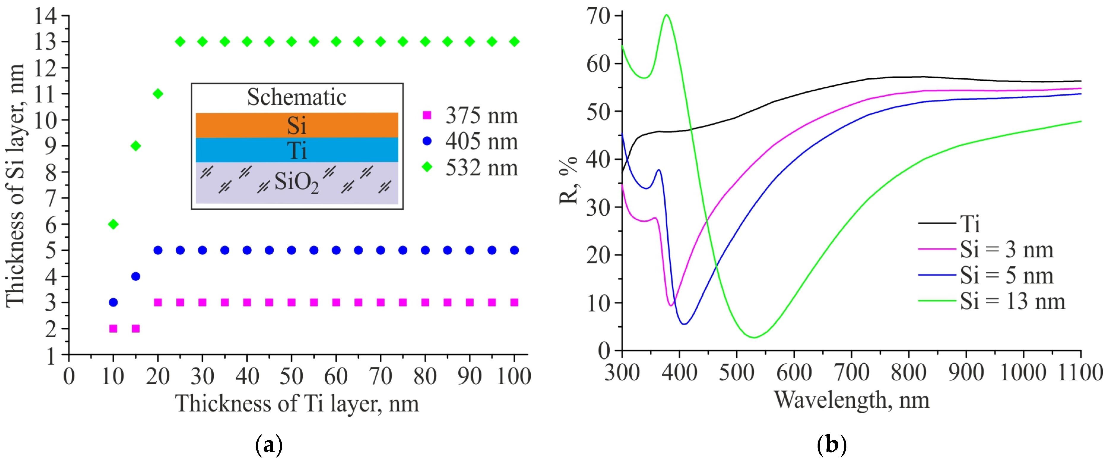
2.1. Theoretical Evaluation of the Parameters and Characteristics of Bi-Layer Si/Ti Films

The characteristics of bi-layer Si/Ti films on fused silica substrates were modeled using a publicly available spectrum calculator [28] with dependences of refractive index and extinction coefficient on wavelength for Ti and crystalline Si.

2.2. Deposition of Ti and Si/Ti Films

The experimental samples of bi-layer Si/Ti films on fused silica substrates (thickness 1 mm, diameter 25.4 mm) were fabricated using the e-beam evaporation system. To do this, the cleaned substrate was placed in a vacuum chamber and heated for 60 min in a vacuum of 10–2 Pa at a temperature of 300 °C. After heating, the chamber was evacuated to a pressure of 8 × 10⁻⁴ Pa, and the temperature was reduced to 250 °C. Then, a Ti layer 50 nm thick was deposited onto the substrate in a vacuum atmosphere. Then, with the same system parameters, the Si capping layer was deposited. The deposition process was controlled via reflectance spectra for the witness glass sample. The criterion for stopping the deposition of the Si capping layer was the achieving a minimum reflection at 532 nm wavelength.

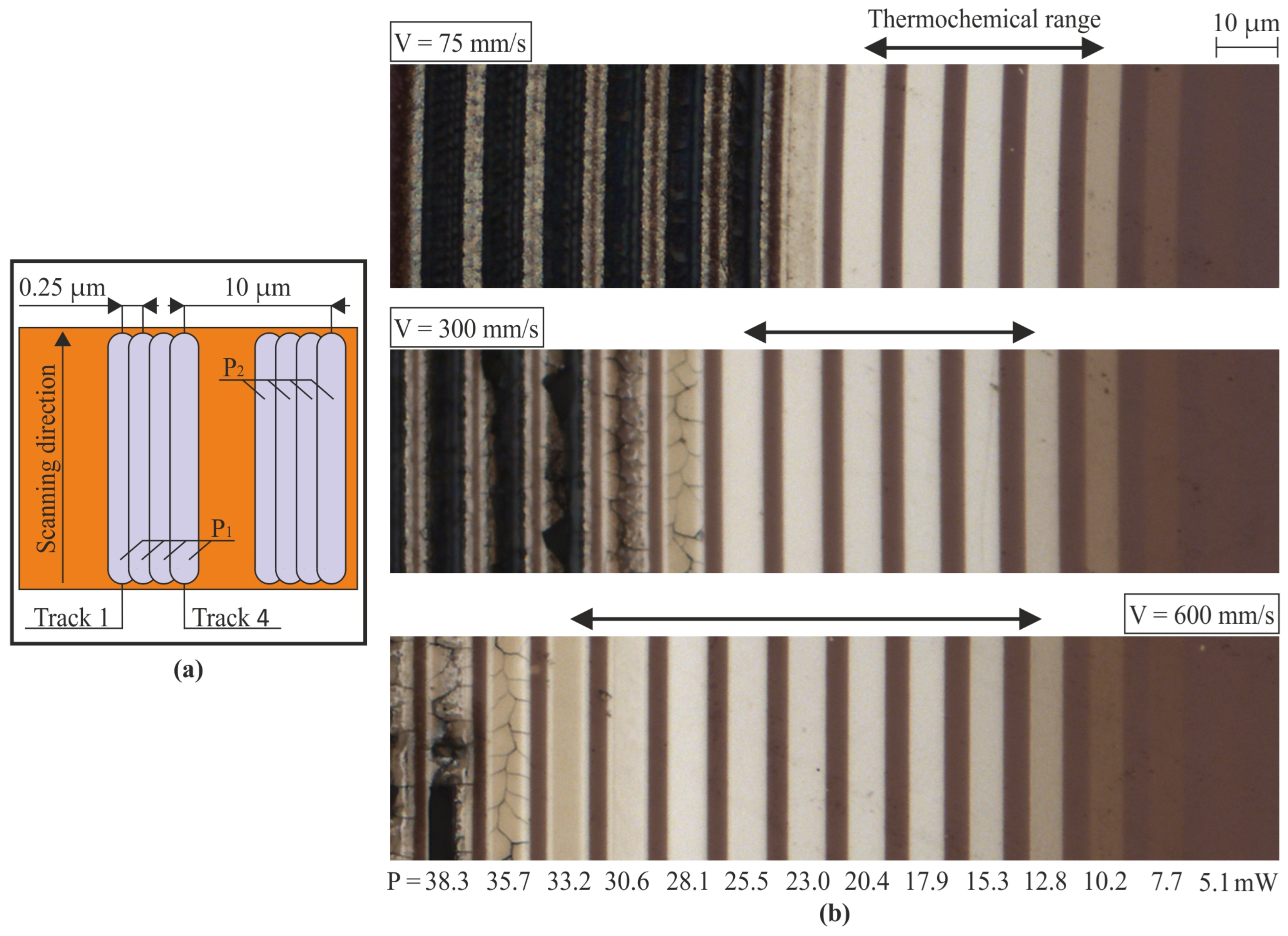
2.3. Formation Test Structures on a Circular Laser Writing System

Experiments with bi-layer Si/Ti films were carried out on a circular laser writing system CLWS-300IAE [4,13,20,29] operating in polar coordinates and were designed for processing of substrates up to 250 mm in diameter and up to 24 mm thick. Figure S1 (Supplementary Materials) shows the simplified circuit of the CLWS-300IAE. This system uses a continuous-wave DPSS laser with a wavelength of 532 nm and a maximum power (P) of 2 W. A flat fused silica substrate with a sputtered bi-layer Si/Ti film was fixed on a faceplate of an air-bearing spindle rotated at 720 rpm. Step-by-step movement of the focusing lens (NA = 0.65) in the radial direction allows one to expose two-dimensional patterns. Radial position of the lens define the linear scanning speed (V) of the focused laser spot, which was 0.7 µm (FWHM) in the experiments.

2.4. Analysis of Structure and Topography of the Films

Structures formed on the film surface of samples were studied with optical microscopy, optical profilometry, atomic force microscopy (AFM) and Raman spectroscopy. Park XE15 AFM and white light interferometer WLI (BMT) were used to analyze profile topography. The local reflectance of the modified films was obtained by processing the pixel intensity distribution on microscopic images from the Zeiss Axio Imager with a green filter installed in the light illumination channel. Registration of microimages was carried out at the same settings of the digital camera parameters. Calibration was carried out with Al mirror.
Raman spectra were acquired using a laboratory-built experimental setup based on the SP-2500i monochromator and the Spec 10:2K CCD detector. Laser radiation with wavelength of 532.1 nm and 1.5 mW power on a sample was used for Raman excitation. The experiment was performed in the backscattering regime using an objective with NA = 0.75, which focuses laser radiation in ~1 μm diameter. A neon discharge lamp was used to calibrate the wavelengths of the measured spectra.

3. Results

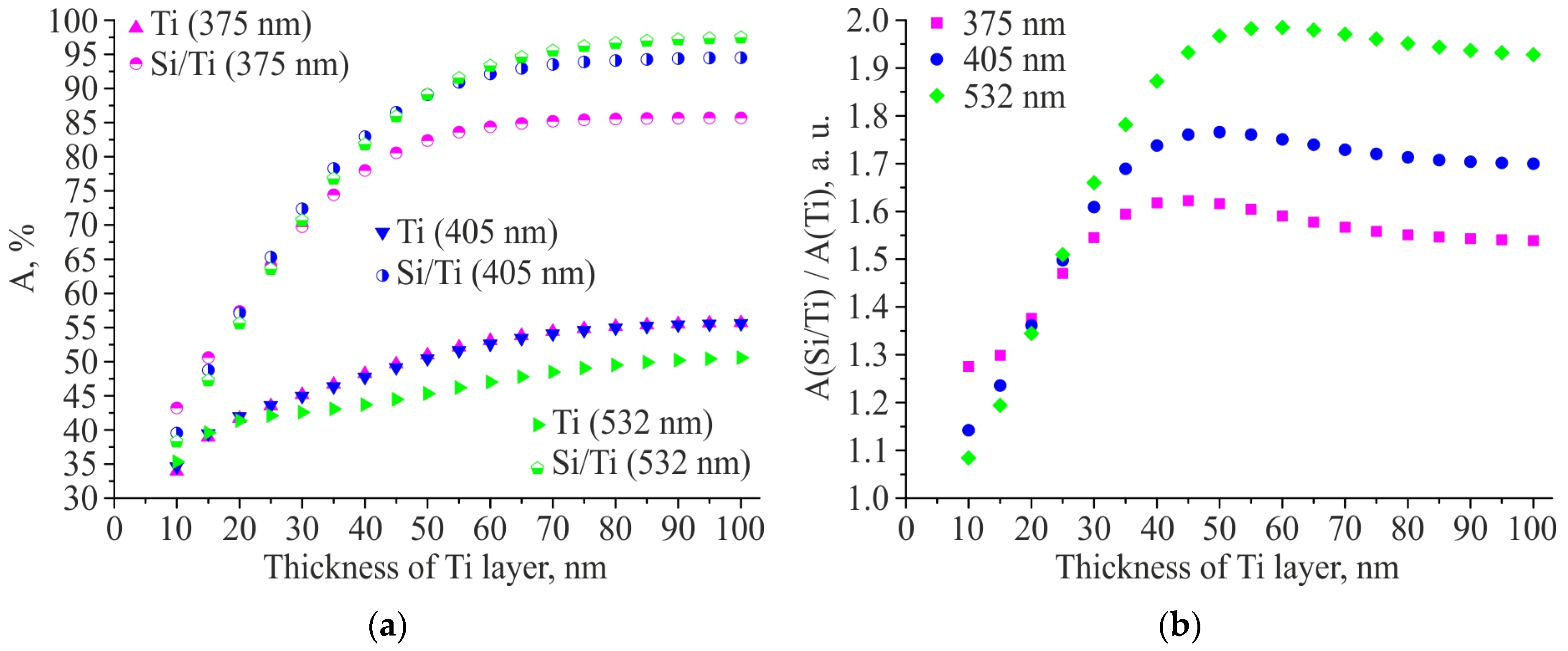
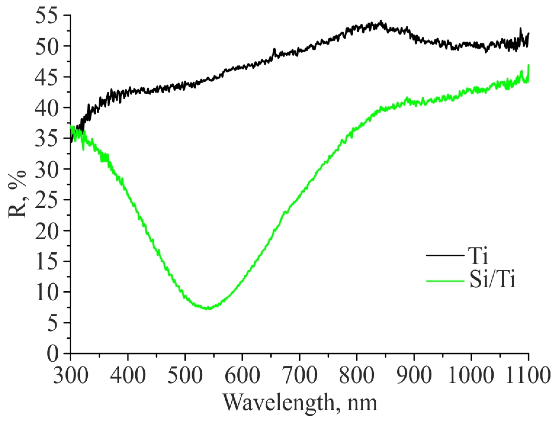
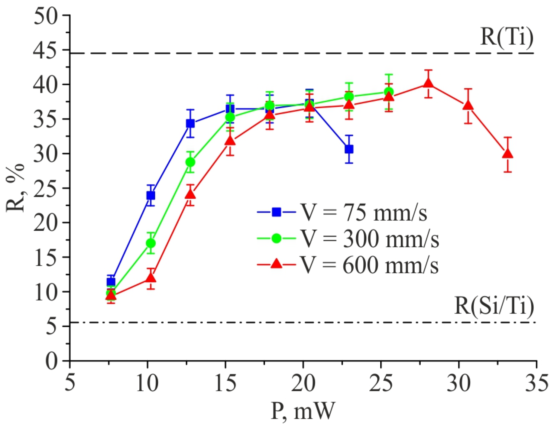
3.1. Optimization of Layer Thicknesses and Experimental Verification

The optimization of the thickness of the Si capping layer deposited on the Ti film was carried out by determining the maximum absorption coefficient (A) of radiation by the bi-layer film at writing beam wavelengths of 532 nm, as well as 375 nm and 405 nm (the wavelengths of laser lithographic systems designed for writing on photoresist). The results of modeling to determine the optimal thickness of the Si capping antireflection layer depending on the thickness of the metal film for the investigated wavelengths are shown in Figure 1a. It can be noted that for Ti film thicknesses in the range from 25 nm to 100 nm, the optimal thickness of the Si capping layer for all of the studied wavelengths does not change and is 3 nm (for λ = 375 nm), 5 nm (for λ = 405 nm) and 13 nm (for λ = 532 nm). Figure 1b shows the calculated reflectance spectra of optimized Si/Ti bi-layer films with a 50 nm Ti layer. An increase in the Si film thickness leads to an increase in the amplitude of the interference peaks for short wavelengths, but as will be shown below, for real Si films, the effect of the interference in the layer decreases due to the significantly higher absorption inherent in amorphous Si films [30].
Figure 2a shows the absorption coefficient characteristics of a bi-layer Si/Ti structure compared to a Ti film. The results obtained show that the use of an antireflection Si coating with a film thickness Ti ≥ 30 nm for all simulated wavelengths makes it possible to achieve an increase in the absorption coefficient by more than 1.5 times compared to a conventional Ti film (Figure 2b). In this case, the greatest increase in the absorption coefficient can be obtained for a wavelength of 532 nm, for which the value of A can be increased by a factor of ~2. In turn, at wavelengths of 375 nm and 405 nm, the increase in radiation absorption can be up by a factor of ~1.62 and ~1.76, respectively. Figure S2 (Supplementary Materials) shows the optical reflectance characteristics of a bi-layer Si/Ti structure compared to a Ti film.
Figure 3 and Figure S3 (Supplementary Materials) shows the experimentally obtained reflectance spectra of the Si/Ti film on a fused silica substrate in comparison with the spectrum of the deposited Ti film on a similar substrate. The measurements of the deposited samples were taken by means of the AvaSpec-ULS2048·16-UA-50 (Avantes) fiber spectrometer and fiber light source AvaLight-DH-S. It should be noted that the experimentally obtained results on the decrease in reflection (ratio R(Ti)/R(Si/Ti) is ~6.1) between the Si/Ti and Ti films at a wavelength of 532 nm are noticeably lower than the theoretically calculated ones (~18.6 in Figure 1b). Nevertheless in the experiment, the absorption of the bi-layer Si/Ti film at a wavelength of 532 nm compared with the Ti film was increased by a factor of ~1.7. It should also be noted that the experimental curve for the Si/Ti film does not have a peak in the range of 350–400 nm, as in the calculated one. This is also explained by the high extinction coefficient in the UV range of the deposited silicon film in comparison with crystalline silicon.

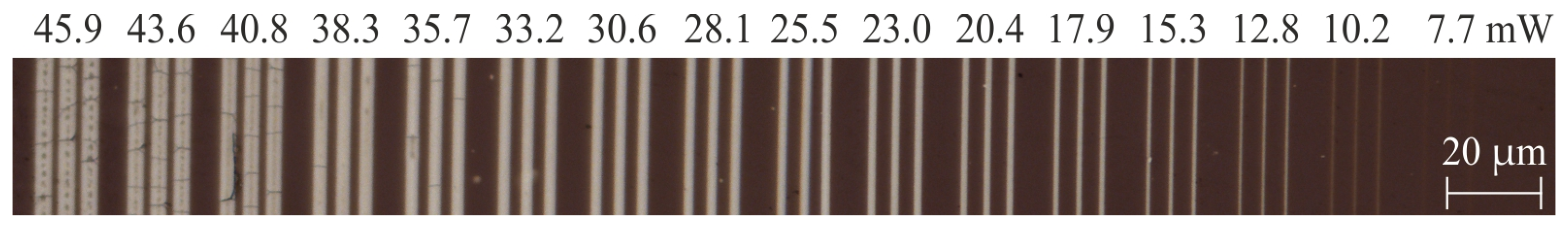
3.2. Direct Laser Writing on Bi-Layer Si/Ti Films

An experimental investigation of laser writing on a bi-layer Si/Ti film deposited on a fused silica substrate was carried out at scanning speeds of the laser writing beam of 75–600 mm/s. Since in the experiments the substrate rotation speed was constant (720 rpm), the maximum writing speed was limited by the radius of the fused silica substrate used (12.7 mm). The maximal radius of the writing field for CLWS-300IAE is 120 mm. This means the linear scanning speed can reach 9000 mm/s.
Groups of tracks (Figure 4a) were written with a gradual decrease in the power (P) of the laser writing beam from 55 to 0 mW. Each group of tracks written at a certain power value was formed by repetition of the tracks of the laser beam with a step in the radial direction equal to 0.25 µm. The step ensures a partial overlay on the exposed areas. The groups of tracks were written with a period of 10 µm relative to each other. Figure 4b shows microimages in reflected light of the irradiated areas of the bi-layer Si/Ti film. The upper boundary of the thermochemical range can be defined as undamaged areas free of cracks and burned spots. The lower boundary can be defined as areas with abrupt decrease in the reflection.
Figure 5 shows the dependencies of the change in reflectance of thermochemically modified areas of the Si/Ti film at a 532 nm wavelength. The plot demonstrates that laser exposure considerably increases the reflectance due to modification of the antireflection capping Si layer.

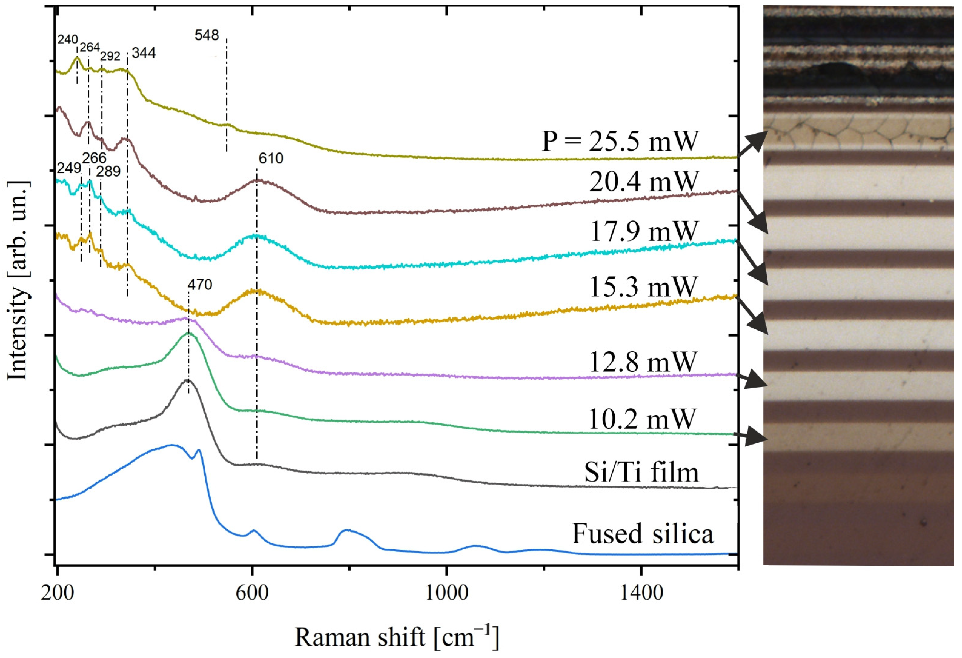
3.3. Raman Spectra Analysis

Figure 6 shows the Raman spectra measured on Si/Ti film areas before laser writing (original Si/Ti film) and after writing with different laser beam power. Microimages of the corresponding areas are depicted on the right side with identification of P. The spectrum for the original Si/Ti film contains a wide peak at 470 cm−1, which is near 480 cm−1, typical for amorphous silicon [31]. The peak disappears when laser beam power exceeds 12.8 mW. The weakening of the peak with increasing laser beam power can be associated with the oxidation of silicon. At laser beam power higher than 15 mW, another pronounced peak at 610 cm−1 appears. It is specific for titanium oxide in the form of rutile [32]. Besides that, a series of peaks in the range 240–344 cm−1 appears due to the formation of titanium silicides. The peaks 240 and 249 are near the well-known peak 243 cm−1 for the C54 phase of TiSi2. The peak 344 is very closed to the peak at 340 cm−1 of crystalline TiSi2 [33]. Unfortunately, the equipment we used to obtain the Raman spectra did not allow us to obtain reliable data for intense lines of titanium silicide below 200 cm−1. Besides titanium silicide, Raman spectra at maximal laser power 25.5 mW (the peak at 548 cm−1) exhibit amorphous TiN formed at high temperature in an N2-containing atmosphere [34].

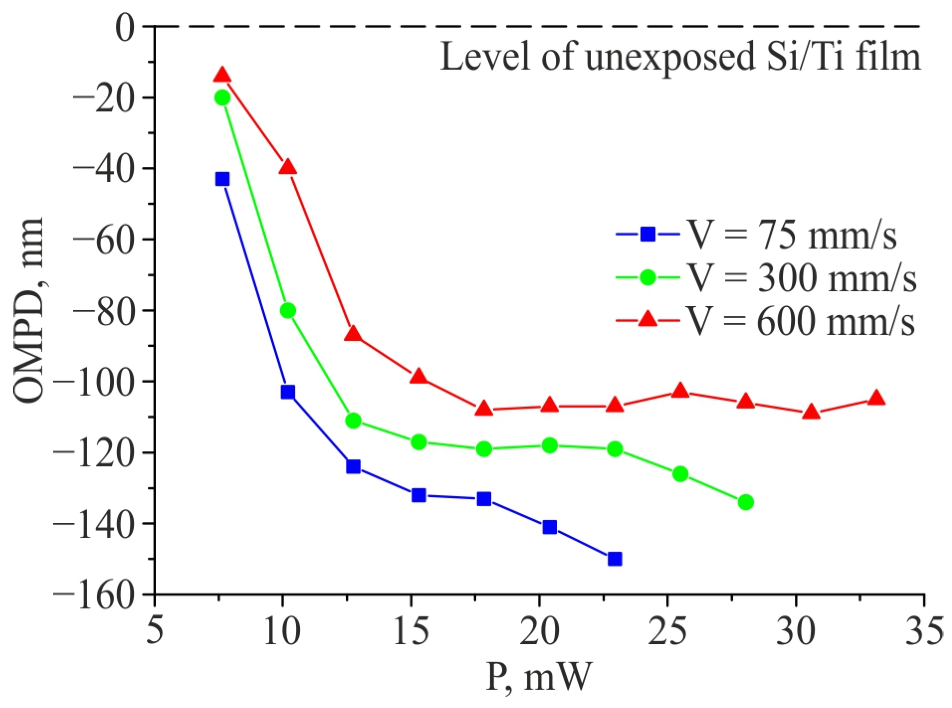
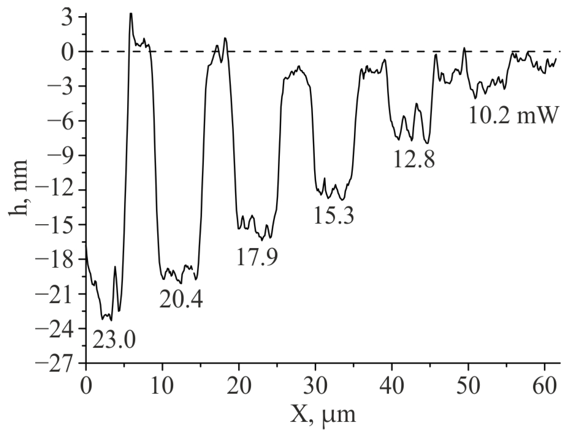
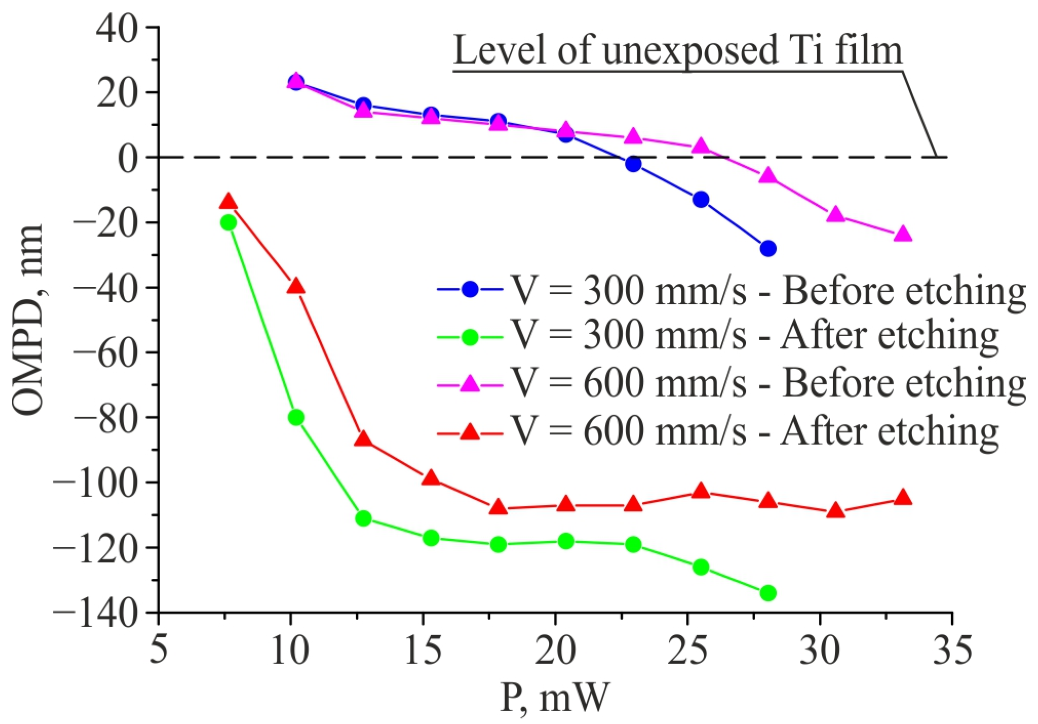
3.4. Measurement of Profile Depth

The white light interferometer was used to determine the optically measured profile depth (OMPD) of the structures formed on Si/Ti films (Figure 7). The OMPD parameter is determined not only by the differences in the profile depth between its protrusions and grooves, but also by the phase shift of light reflected from various materials on top of the protrusions and on the bottom of the grooves. That is, the OMPD parameter is proportional to the so-called position-dependent phase changes (PDPCs). The results of measuring the exposed areas showed an increase in the OMPD of the formed structures up to ~150 nm. The maximum value of the OMPD of the structures in the experiments depended on the writing rate, with lower writing rates resulting in higher OMPD.
Figure 8 shows AFM measurements of test structures written at a scanning speed of 75 mm/s. It can be observed that the physical depth (h) of the tracks is significantly less than the OMPD (about six times). In this case, unlike direct laser writing on Ti films, which leads to the formation of oxide protrusions above the initial level of the metal film due to thermochemical reaction, grooves are formed in the bi-layer Si/Ti film.
It can be noted in Figure 5 and Figure 7 that when the power of the laser writing beam exceeds ~15 mW, the reflectance and OMPD of the exposed areas reaches the limiting values, which practically do not change with a further increase in power (until approaching the melting threshold of the material). At the same time, changing the power in this range allows for adjustment of the duty cycle of the formed structures (Figure 9).

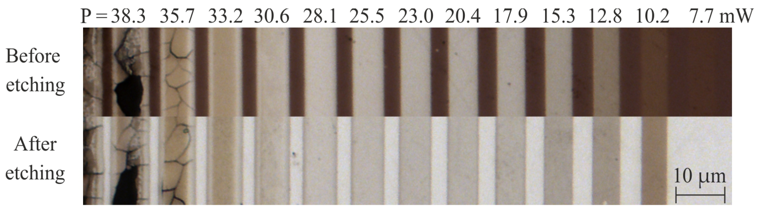
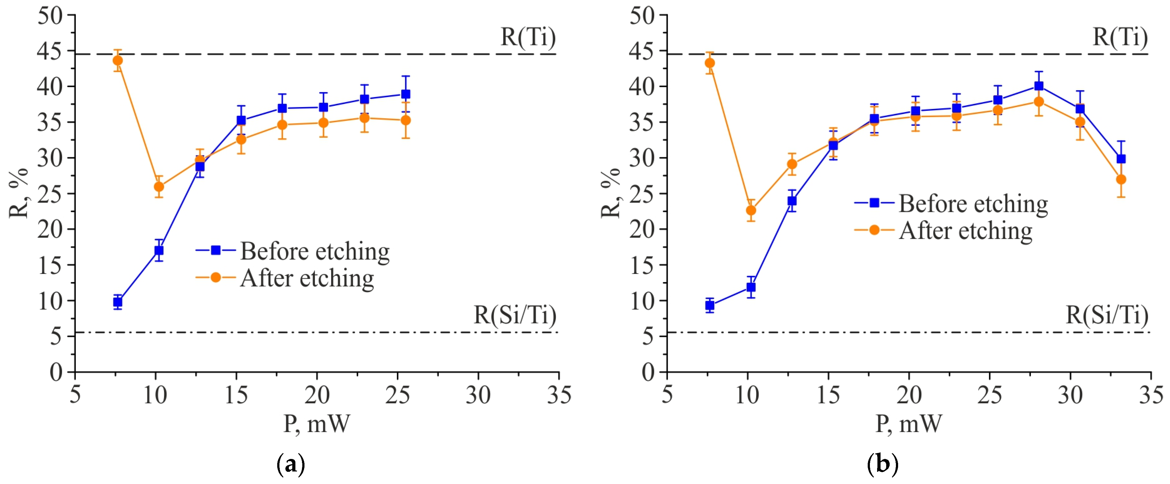
3.5. Etching the Capping Si Layer from the Structures Formed on the Si/Ti Film

To conduct experiments on the manifestation of structures written on a Si/Ti film, structures formed at writing speeds of 300 mm/s and 600 mm/s were cut out from the investigative sample. Next, in a 30% KOH solution at a liquid etchant temperature of ~110 °C for ~40 s, the Si capping layer was etched from the cut sample. This etchant was chosen due to the fact that it does not etch titanium silicide and SiO2 compounds, which presumably occur in thermochemically modified areas. Figure 10 shows microimages of test structures before and after etching of the Si capping layer. Figure 11 presents the reflectance changes from exposed areas before and after etching. According to the graphs of changes in the reflectance of the exposed areas, it can be noted that at powers below 12.8 mW (for V = 300 mm/s) and below 15.3 mW (for V = 600 mm/s), a drop in reflectance from the irradiated areas is observed with increasing power writing. However, the obtained reflectance values are higher than before Si etching. This means that the Si capping layer is partially modified on these structures under thermochemical action. With further power increase, the entire capping layer of silicon is modified, and therefore liquid etching does not affect the reflectance change of the exposed areas.
Figure 12 presents the data on the change of the OMPD of the modified areas. It can be observed that the effect of increasing OMPD disappears when the Si film is etched. The monotonic change in the OMPD of the exposed areas relative to the surface of the non-irradiated titanium film after Si etching in Figure 12 ranges from +20 nm (above the Ti surface) to −20 nm (below the Ti surface). This can be explained by changes in the phase shift of light reflected from areas with different chemical composition and thickness of the modified layer due to the different power of the laser beam during writing.

4. Discussion

The studies performed have shown that the deposition of a silicon layer on a titanium film makes it possible to obtain various beneficial effects in thermochemical laser writing: antireflection increasing optical absorption of the writing laser beam, protection against oxidation at storage in room conditions and the formation of chemically resistive silicide and oxide layers under laser heating. According to modeling results, the optical absorption at a wavelength of 532 nm is increased by a factor of ~1.7 compared to the laser oxidation of bare titanium film. Using more complicated thermochemical reactions due to introducing the Si capping layer makes it possible to increase the speed of thermochemical laser writing on a Ti-containing film by at least three times compared to bare Ti films [20].
However, a more complicated film structure results in some effects with respect to laser writing which need to be explained. One of these effects is the formation of grooves (as shown in the AFM profile in Figure 8) instead of protrusions, which are typical for metal oxidation under laser heating. It is possible that the formation of grooves is associated with several different reasons at different laser beam power levels. High-temperature annealing of an oxygen-free Ti film can be accompanied by structure ordering and corresponding thickness reduction. Laser heating of the bi-layer Si/Ti film results in the formation of titanium silicide [35] and/or silicon oxide [36] compounds on the surface. At temperatures of 620–720 °C, the formation of a Ti5Si3 compound is possible at the titanium–silicon interface, and at higher temperatures, a TiSi2 compound is possible [37,38]. Titanium silicides have considerably higher density than silicon, which can also result in the formation of grooves under laser action. Additionally, the process of formation of titanium silicides can be accompanied by a decrease in the volume of the bi-layer Si/Ti film due to the presence of stresses in the initial thin deposited films [37]. At heating temperatures of the Si/Ti film above 700 °C, oxidation of the silicon capping layer can take place [36] and influences profile depth. To test the applicability of known data to our experiments, it would be useful to estimate the temperatures reached. This can be done with respect to the titanium melting point of 1941 °K, at which significant damage to the film surface occurs. For example, in Figure 4b, the first damaged black vertical zone after the thermochemical range corresponds to a laser beam power of 25.5 mW at a scan rate of 75 mm/s. Taking the temperature reached in this zone as 1941 °K, one can estimate the lower temperature of the thermochemical range as 776 °K (or ~500 °C), considering it to be proportional to the beam power. Such a simplified dependence is quite justified if we consider the thermophysical parameters of the material to be independent of temperature. Similarly, an estimate of the upper limit of the thermochemical range gives approximately 1550 °K (or ~1280 °C). Therefore, we can conclude that the temperature ranges known from the published literature for the formation of titanium silicides are in good agreement with the experimental results obtained.
During laser heating of a bi-layer Si/Ti film, besides the formation of a titanium silicide composition at the titanium–silicon interface, titanium oxide can also form at higher laser beam power. The reactions have been proved in our analysis of Raman spectra (Raman spectra in Figure 6), mainly corresponding to published results [39]. An analysis of the structures formed on Si/Ti bi-layer films showed that, upon reaching a certain value of the writing power, the OMPD (Figure 7) and reflectance (Figure 5) from thermochemically modified areas reach a threshold value and, with a further increase in power, practically do not change (until they come close to damaging the film). The reason for this effect can be either the formation of a silicide layer with a thickness exceeding the thickness of the skin layer, or the complete consumption of the silicon layer during the thermochemical reaction. Thus, during laser writing on Si/Ti films, there is a fairly wide range of writing beam power within which the parameters of the OMPD and reflectance of the modified structures change insignificantly. In this case, changing the power in this range allows one to adjust the duty cycle of the formed structures (Figure 9).
An analysis of the OMPD proportional to the PDPC of the structures formed on the Si/Ti film during thermochemical laser writing showed an increase in the OMPD between the exposed and unexposed areas of the Si/Ti film of up to ~150 nm. The maximum value of the OMPD of the structures in the experiments depended on the writing speed: the lower the scanning speed, the higher the OMPD. In this case, the structure height measured with an atomic force microscope did not exceed ~25 nm. In this case, after removing the Si capping layer from the written samples via selective etchant, the effect of increasing the OMPD in the exposed areas disappeared. The results show that the Si capping layer plays a key role in increasing the phase shift between exposed and unexposed areas on the Si/Ti film. This is explained by the fact that the electrical and optical properties of titanium silicide are close to those of metals. For example, TiSi2 has a reflectance of ~40% and higher at a thickness of more than 12 nm, according to calculations on a publicly available spectrum calculator [28]. Therefore, when light is reflected from it, a significant phase shift occurs in relation to silicon. After removing the unexposed Si capping layer, the phase shift between the silicide surface and titanium surface is mainly defined by the real profile depth (because two metal-like surfaces are involved in the measurement).
An analysis of the change of reflectance (Figure 11) from the exposed areas before and after etching the capping Si layer showed that at powers of the laser writing beam below 12.8 mW (for V = 300 mm/s) and below 15.3 mW (for V = 600 mm/s), only a part of the Si capping layer undergoes thermochemical modification. Part of the unmodified silicon layer for these structures was etched in a hot liquid etchant. With a further increase in power, the entire capping layer of silicon was modified, and therefore liquid etching did not affect the change in the reflectance of the exposed areas.
To check the applicability of the proposed material and technique for the fabrication of real diffractive structures, reflective diffraction gratings with a period of 10 μm were written on a bi-layer Si/Ti film via single-stage direct laser writing. The scanning speed during grating writing was 450 mm/s, and the power of the writing beam was 17.8 mW and 12.8 mW. The OMPD of the formed gratings measured at the WLI was ~120 nm and ~80 nm, respectively. The speed of writing diffractive structures is between the speeds investigated in the work of 300 mm/s and 600 mm/s (Figure 8). According to the values of the measured OMPD of the gratings, it can be concluded that the power value of 17.8 mW is close to the threshold in terms of achieving the maximum OMPD for a given write speed. Table 1 shows the measured diffraction efficiency (DE) of the formed gratings in reflected light for the first diffraction order at probe beam wavelengths of 532 nm and 405 nm. DE was calculated with respect to the power of the probe beam incident on the grating; i.e., the obtained values include reflection losses. This method of determining the diffraction efficiency is necessary for the use of DOE in interferometric optical testing of aspherical surfaces.
At first glance, the measured values are rather low, but the corresponding DE of amplitude chromium DOEs on glass substrates operating in reflection is about 5% due to the low reflection of chromium films. Such amplitude-reflective DOEs are used for optical testing of steep aspherical surfaces due to the impossibility of manufacturing phase DOEs with too narrow (period less than 2000 nm) diffractive zones and to minimize the contribution of the substrate to wavefront distortion.

5. Conclusions

The obtained results demonstrate that using an antireflection silicon layer makes it possible to increase the rate of thermochemical laser writing on a Ti film to at least 600 mm/s. It can also be assumed that this value is not limiting. In future experiments we are planning to test the applicability of Si/Ti films for laser writing at scanning speeds of up to 5000–9000 mm/s.
The diffraction efficiency of DOEs fabricated on Si/Ti films can be increased if the initial thickness of Si films is optimized not to increase absorption at the wavelength of the writing beam, but to increase the reflectance of the laser-modified film under the condition of the OMPD equal to a quarter of the wavelength of the light used for measurements.
The proposed technology is single-stage and does not contain any liquid developing or plasma etching of the pattern that introduce errors and distortions. The reflectance and geometrical sizes of fabricated patterns can be measured in reflected light directly during laser writing. Such a method of direct photo-electric in situ testing cannot be implemented either for direct laser writing on a photoresist or for thermochemical laser writing on chromium films due to the very small change in the reflection of the recording layer for these technologies. Therefore, the proposed technology has considerable advantages in fabricating reflective binary DOEs with high numerical aperture compared to known laser technologies.
The developed technology of laser writing on bi-layer Si/Ti films can also be applied for fabrication of binary phase transmissive diffractive elements if additional etching processes are used. The etching of the silicon capping layer and then the selective etching of the unexposed titanium film can make it possible to form silicide or silicide/titanium masks on the fused silica substrate. This can be achieved, for example, through wet etching [40]. At the next step, reactive ion etching in a mixture of CF4 and H2 can be used for etching of a fused silica substrate through a silicide/titanium mask. The ratio of SiO2:TiSi2 etching rates is more than 40:1 [41]. This is higher than the selectivity of the standard chromium technology, for which the corresponding ratio of SiO2:Cr etching rates is ~30:1. For example, to produce binary phase computer-generated holograms operating in optical testing at a wavelength of 633 nm, the diffractive structure in fused silica must have a depth of 693 nm and therefore the silicide mask should have a thickness of at least 20 nm. This is quite an attainable value for the thermochemical laser formation of a silicide mask. Nevertheless, the technology described above without etching processes looks more attractive, although its scope is limited to reflective binary DOEs.

Supplementary Materials

The following supporting information can be downloaded at: https://www.mdpi.com/article/10.3390/photonics10070771/s1, Figure S1. Simplified circuit of the CLWS-300IAE; Figure S2. Reflectance characteristics: (a) Comparison of R(Si/Ti) and R(Ti); (b) Ratio R(Ti)/R(Si/Ti); Figure S3. Reflectance spectrums of Si/Ti films depending on the thickness of the capping Si layer.

Author Contributions

Conceptualization, D.A.B., R.I.K. and V.P.K.; methodology, V.P.K.; software, D.A.B.; validation, D.A.B. and R.I.K.; formal analysis, D.A.B., R.I.K. and V.P.K.; investigation, D.A.B., R.I.K., V.P.K. and K.A.O.; resources, D.A.B.; data curation, D.A.B., R.I.K. and V.P.K.; writing—original draft preparation, D.A.B. and V.P.K.; writing—review and editing, D.A.B. and V.P.K.; visualization, D.A.B.; supervision, D.A.B. and V.P.K.; project administration, D.A.B.; funding acquisition, D.A.B. All authors have read and agreed to the published version of the manuscript.

Funding

This research was funded by Russian Science Foundation, grant No. 22-79-00049.

Data Availability Statement

The data related with this work are not publicly available but can be obtained upon reasonable request from the corresponding author.

Acknowledgments

The equipment of the Central Research Center “Spectroscopy and Optics” of the IA&E SB RAS and Core Facilities VTAN NSU were used in the research. The authors are grateful to Anatoly I. Malyshev and Alexander R. Sametov for their help in carrying out the experiments.

Conflicts of Interest

The authors declare no conflict of interest. The funders had no role in the design of the study; in the collection, analyses or interpretation of data; in the writing of the manuscript or in the decision to publish the results.

References

  1. d’Auria, L.; Huignard, J.P.; Roy, A.M.; Spitz, E. Photolithographic fabrication of thin film lenses. Opt. Commun. 1972, 5, 232–235. [Google Scholar] [CrossRef]
  2. Gale, M.T.; Rossi, M.; Pedersen, J.; Schuetz, H. Fabrication of continuous-relief micro-optical elements by direct laser writing in photoresists. Opt. Eng. 1994, 33, 3556–3566. [Google Scholar] [CrossRef]
  3. Sohn, J.S.; Lee, M.B.; Kim, W.C.; Cho, E.H.; Kim, T.W.; Yoon, C.Y.; Park, N.C.; Park, Y.P. Design and fabrication of diffractive optical elements by use of gray-scale photolithography. Appl. Opt. 2005, 44, 506–511. [Google Scholar] [CrossRef] [PubMed]
  4. Veiko, V.P.; Korolkov, V.P.; Poleshchuk, A.G.; Sinev, D.A.; Shakhno, E.A. Laser technologies in micro-optics. Part 1. Fabrication of diffractive optical elements and photomasks with amplitude transmission. Optoelectron. Instrum. Data Process. 2017, 53, 474–483. [Google Scholar] [CrossRef]
  5. Korolkov, V.P.; Nasyrov, R.K.; Khomutov, V.N.; Belousov, D.A.; Kutz, R.I. Development of methods for the formation and control of a given distribution of the photoresist thickness for conformal correctors fabrication. In Optical Design and Testing XI; SPIE: Bellingham, WA, USA, 2021; Volume 11895, p. 118951J. [Google Scholar]
  6. Poleshchuk, A.G.; Kutanov, A.A.; Bessmeltsev, V.P.; Korolkov, V.P.; Shimanskii, R.V.; Malyshev, A.I.; Matochkin, A.E.; Goloshevskii, N.V.; Makarov, K.V.; Makarov, V.P.; et al. Microstructuring of optical surfaces: Technology and device for direct laser writing of diffractive structures. Optoelectron. Instrum. Data Process. 2010, 46, 171–180. [Google Scholar] [CrossRef]
  7. Veiko, V.; Yarchuk, M.; Zakoldaev, R.; Gedvilas, M.; Račiukaitis, G.; Kuzivanov, M.; Baranov, A. Picosecond laser registration of interference pattern by oxidation of thin Cr films. Appl. Surf. Sci. 2017, 404, 63–66. [Google Scholar] [CrossRef]
  8. Clark, P.P.; Londono, C. Production of kinoforms by single point diamond machining. Opt. News 1989, 15, 39–40. [Google Scholar] [CrossRef]
  9. Saastamoinen, T.; Väyrynen, J.; Mutanen, J.; Tuovinen, H.; Eronen, A.; Mönkkönen, K.; Kuittinen, M. Fabrication of hybrid optical line generator by direct machining. Opt. Express. 2018, 26, 2335–2340. [Google Scholar] [CrossRef] [Green Version]
  10. Fang, F.Z.; Zhang, X.D.; Weckenmann, A.; Zhang, G.X.; Evans, C. Manufacturing and measurement of freeform optics. CIRP Ann. Manuf. Technol. 2013, 62, 823–846. [Google Scholar] [CrossRef]
  11. Koronkevich, V.P.; Poleshchuk, A.G.; Churin, E.G.; Yurlov, Y.I. Laser thermochemical technology for synthesizing optical diffraction elements utilizing chromium films. Sov. J. Quantum Electron. 1985, 15, 494. [Google Scholar] [CrossRef]
  12. Veiko, V.P.; Sinev, D.A.; Shakhno, E.A.; Poleshchuk, A.G.; Sametov, A.R.; Sedukhin, A.G. Researching the features of multibeam laser thermochemical recording of diffractive microstructures. Comput. Opt. 2012, 36, 562–571. [Google Scholar]
  13. Poleshchuk, A.G.; Churin, E.G.; Koronkevich, V.P.; Korolkov, V.P.; Kharissov, A.A.; Cherkashin, V.V.; Kiryanov, V.P.; Kiryanov, A.V.; Kokarev, S.A.; Verhoglyad, A.G. Polar coordinate laser pattern generator for fabrication of diffractive optical elements with arbitrary structure. Appl. Opt. 1999, 38, 1295–1301. [Google Scholar] [CrossRef] [PubMed]
  14. Korolkov, V.P.; Sedukhin, A.G.; Mikerin, S.L. Technological and optical methods for increasing the spatial resolution of thermochemical laser writing on thin metal films. Opt. Quantum Electron. 2019, 51, 389. [Google Scholar] [CrossRef]
  15. Gorbunov, A.A.; Eichler, H.; Pompe, W.; Huey, B. Lateral self-limitation in the laser-induced oxidation of ultrathin metal films. Appl. Phys. Lett. 1996, 69, 2816–2818. [Google Scholar] [CrossRef]
  16. Wang, Y.; Miao, J.; Tian, Y.; Guo, C.; Zhang, J.; Ren, T.; Liu, Q. TiO2 micro-devices fabricated by laser direct writing. Opt. Express. 2011, 19, 17390–17395. [Google Scholar] [CrossRef] [PubMed]
  17. Shakhno, E.A.; Sinev, D.A.; Kulazhkin, A.M. Features of laser oxidation of thin films of titanium. J. Opt. Technol. 2014, 81, 298–302. [Google Scholar] [CrossRef]
  18. Xia, F.; Jiao, L.; Wu, D.; Li, S.; Zhang, K.; Kong, W.; Yun, M.; Liu, Q.; Zhang, X. Mechanism of pulsed-laser-induced oxidation of titanium films. Opt. Mater. Express. 2019, 9, 4097–4103. [Google Scholar] [CrossRef]
  19. Korolkov, V.P.; Nasyrov, R.K.; Sametov, A.R.; Malyshev, A.I.; Belousov, D.A.; Mikerin, S.L.; Kuts, R.I. Direct laser writing of high-NA computer-generated holograms on metal films of the titanium group and chromium. In Holography, Diffractive Optics, and Applications IX; SPIE: Bellingham, WA, USA, 2019; Volume 11188, p. 111880R. [Google Scholar]
  20. Korolkov, V.P.; Sedukhin, A.G.; Belousov, D.A.; Shimansky, R.V.; Khomutov, V.N.; Mikerin, S.L.; Spesivtsev, E.V.; Kutz, R.I. Increasing the spatial resolution of direct laser writing of diffractive structures on thin films of titanium group metals. In Holography: Advances and Modern Trends VI; SPIE: Bellingham, WA, USA, 2019; Volume 11030, p. 110300A. [Google Scholar]
  21. Belousov, D.A.; Bronnikov, K.A.; Okotrub, K.A.; Mikerin, S.L.; Korolkov, V.P.; Terentyev, V.S.; Dostovalov, A.V. Thermochemical Laser-Induced Periodic Surface Structures Formation by Femtosecond Laser on Hf Thin Films in Air and Vacuum. Materials 2021, 14, 6714. [Google Scholar] [CrossRef]
  22. Korolkov, V.P.; Nasyrov, R.K.; Sedukhin, A.G.; Belousov, D.A.; Kuts, R.I. New methods of manufacturing high-aperture computer-generated holograms for reference wavefront shaping in interferometry. Optoelectron. Instrum. Data Process. 2020, 56, 140–149. [Google Scholar] [CrossRef]
  23. Korolkov, V.P.; Kuts, R.I.; Malyshev, A.I.; Belousov, D.A.; Matochkin, A.E. Usage of dry processes for the formation of diffractive structures on Ti and Ti/Si films. In Optical Fabrication, Testing, and Metrology VII; SPIE: Bellingham, WA, USA, 2021; Volume 11873, p. 1187307. [Google Scholar]
  24. Hass, G.; Bradford, A.P. Optical properties and oxidation of evaporated titanium films. JOSA 1957, 47, 125–129. [Google Scholar] [CrossRef]
  25. Polasko, K.J.; Griffing, B.F. Thin silicon films used as antireflection coatings for metal coated substrates. In Advances in Resist Technology and Processing III; SPIE: Bellingham, WA, USA, 1986; Volume 631, pp. 180–186. [Google Scholar]
  26. Naghshine, B.B.; Kiani, A. Laser processing of thin-film multilayer structures: Comparison between a 3D thermal model and experimental results. Beilstein J. Nanotechnol. 2017, 8, 1749–1759. [Google Scholar] [CrossRef] [PubMed] [Green Version]
  27. Ihlemann, J.; Rubahn, K.; Thielsch, R. Laser ablation patterning of dielectric layer stacks for 193-nm mask fabricaton. In Second International Symposium on Laser Precision Microfabrication; SPIE: Bellingham, WA, USA, 2002; Volume 4426, pp. 437–440. [Google Scholar]
  28. Filmetrics—Reflectance Calculator. Available online: https://www.filmetrics.com/reflectance-calculator (accessed on 25 June 2023).
  29. Poleshchuk, A.G.; Korolkov, V.P. Laser writing systems and technologies for fabrication of binary and continuous relief diffractive optical elements. In International Conference on Lasers, Applications, and Technologies 2007: Laser-assisted Micro-and Nanotechnologies; SPIE: Bellingham, WA, USA, 2007; Volume 6732, p. 67320X. [Google Scholar]
  30. Refractiveindex.info. Available online: https://refractiveindex.info/?shelf=main&book=Si&page=Pierce (accessed on 25 June 2023).
  31. Bronnikov, K.; Dostovalov, A.; Cherepakhin, A.; Mitsai, E.; Nepomniaschiy, A.; Kulinich, S.A.; Zhizhchenko, A.; Kuchmizhak, A. Large-scale and localized laser crystallization of optically thick amorphous silicon films by near-IR femtosecond pulses. Materials 2020, 13, 5296. [Google Scholar] [CrossRef]
  32. Parker, J.C.; Siegel, R.W. Calibration of the Raman spectrum to the oxygen stoichiometry of nanophase TiO2. Appl. Phys. Lett. 1990, 57, 943–945. [Google Scholar] [CrossRef]
  33. Vála, L.; Vavruňková, V.; Jandová, V.; Křenek, T. Laser ablation of silicon monoxide and titanium monoxide in liquid: Formation of mixed colloidal dispersion with photocatalytic activity. J. Phys. Conf. Ser. 2020, 1527, 012046. [Google Scholar] [CrossRef]
  34. Morgan, A.E.; Broadbent, E.K.; Ritz, K.N.; Sadana, D.K.; Burrow, B.J. Interactions of thin Ti films with Si, SiO2, Si3N4, and SiOxNy under rapid thermal annealing. J. Appl. Phys. 1988, 64, 344–353. [Google Scholar] [CrossRef]
  35. Levy, D.; Ponpon, J.P.; Grob, A.; Grob, J.J.; Stuck, R. Rapid thermal annealing and titanium silicide formation. Appl. Phys. A 1985, 38, 23–29. [Google Scholar] [CrossRef]
  36. Micheli, F. Argon Laser Oxidation of Silicon. Ph.D. Thesis, University of London United Kingdom, London, UK, 1990. [Google Scholar]
  37. Pilipenko, V.A.; Anishchik, V.M.; Ponomar, V.N.; Pilipenko, I.V. Electrophysical and mechanical properties of titanium disilicide produced by using rapid heat treatment. Bull. BSU 2001, 2, 29–34. [Google Scholar]
  38. Pilipenko, V.A.; Ponomar, V.N.; Ponariadov, V.V.; Pilipenko, I.V.; Gorushko, V.A. Features of the structure and phase transitions in the titanium-silicon system during the rapid thermal treatment. In Proceedings of the 4-th International Conference «Interaction of Radiation with Solids», Minsk, Belarus, 3–5 October 2001. [Google Scholar]
  39. Chen, S.Y.; Shen, Z.X.; Chen, Z.D.; See, A.K.; Chan, L.H.; Zhang, T.J.; Tee, K.C. Laser-induced formation of titanium silicides. Surf. Interface Anal. 1999, 28, 200–203. [Google Scholar] [CrossRef]
  40. Walker, P.; Tarn, W.H. CRC Handbook of Metal Etchants; CRC Press LLC: Boca Raton, FL, USA, 1990. [Google Scholar]
  41. Jaso, M.A.; Robey, S.W.; Oehrlein, G.S. Etch Selectivity of Silicon Dioxide over Titanium Silicide Using CF 4/H 2 Reactive Ion Etching. J. Electrochem. Soc. 1989, 136, 3812–3815. [Google Scholar] [CrossRef]
Figure 1. Optimization of the antireflection Si layer thickness deposited on the Ti film: (a) Optimum Si layer thickness versus Ti layer thickness; (b) Examples of reflectance spectra (thickness Ti = 50 nm) for silicon layers of various thicknesses.
Photonics 10 00771 g001
Figure 2. Absorption coefficient characteristics: (a) Comparison of A(Si/Ti) and A(Ti); (b) Absorption coefficient ratio A(Si/Ti)/A(Ti).
Photonics 10 00771 g002
Figure 3. Reflectance spectra of the deposited films.
Photonics 10 00771 g003
Figure 4. Test structures written on a bi-layer Si/Ti film: (a) Scheme of laser writing of test structures; (b) Microimages (in reflected light) of test structure writings at different powers during direct laser writing on a bi-layer Si/Ti film.
Photonics 10 00771 g004
Figure 5. Change in reflectance (at 532 nm wavelength) from the exposed areas of the Si/Ti film.
Photonics 10 00771 g005
Figure 6. Raman spectra for Si/Ti film areas (right side) exposed at different laser beam power levels (V = 150 mm/s).
Photonics 10 00771 g006
Figure 7. Optically measured profile depth of structures fabricated on Si/Ti films.
Photonics 10 00771 g007
Figure 8. AFM profilogram of the formed structures (V = 75 mm/s).
Photonics 10 00771 g008
Figure 9. Image of single tracks on a Si/Ti film depending on the power of the laser writing beam (V = 300 mm/s).
Photonics 10 00771 g009
Figure 10. Microimages (in reflection) of test writing (V = 600 mm/s) before and after etching of the capping silicon layer.
Photonics 10 00771 g010
Figure 11. Change of reflectance at a wavelength of 532 nm from exposed areas before and after etching of the capping silicon layer: (a) V = 300 mm/s; (b) V = 600 mm/s.
Photonics 10 00771 g011
Figure 12. Optically measured profile depth of structures written on a bi-layer Si/Ti film before and after etching of the silicon capping layer.
Photonics 10 00771 g012
Table 1. Diffraction efficiency of the first diffraction order in reflected light measured for test gratings with a period of 10 μm written on a Si/Ti film.
Probe Beam Wavelength (λ), nmWriting Power (P), mWDE, %
53217.81.4
12.80.8
40517.82.1
12.81.0
Disclaimer/Publisher’s Note: The statements, opinions and data contained in all publications are solely those of the individual author(s) and contributor(s) and not of MDPI and/or the editor(s). MDPI and/or the editor(s) disclaim responsibility for any injury to people or property resulting from any ideas, methods, instructions or products referred to in the content.

