Lithography-Free Bismuth Metamaterials for Advanced Light Manipulation

Abstract
:1. Introduction
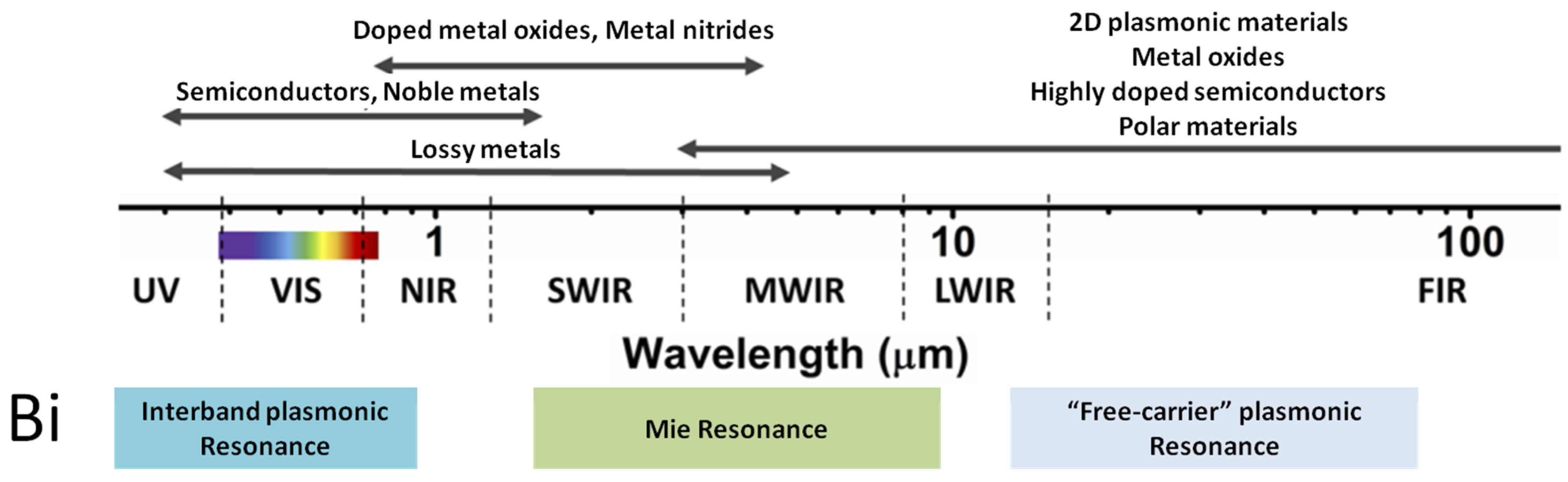
2. Fundamental Optoelectronic Properties of Bi
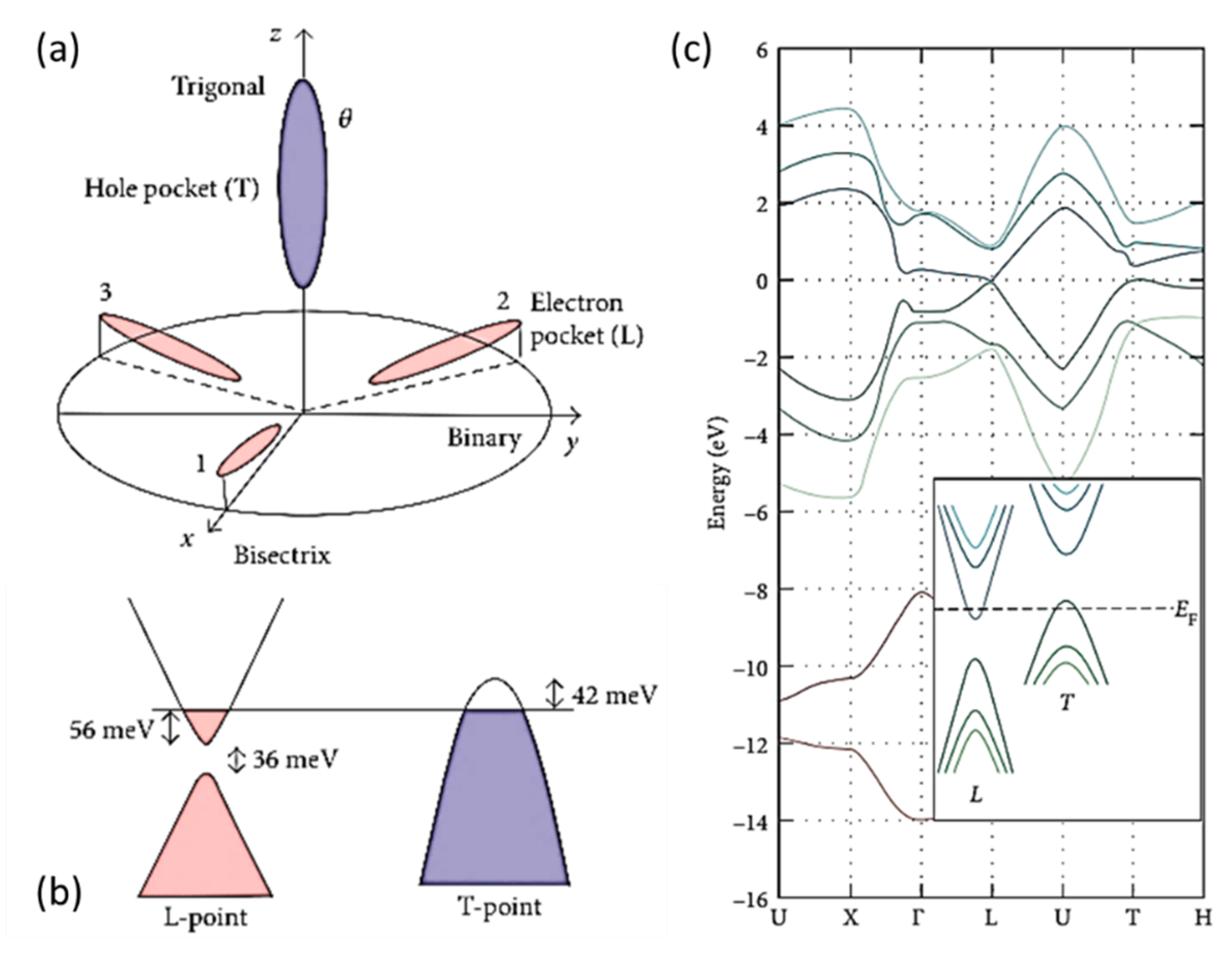
2.1. Electronic Band Structure
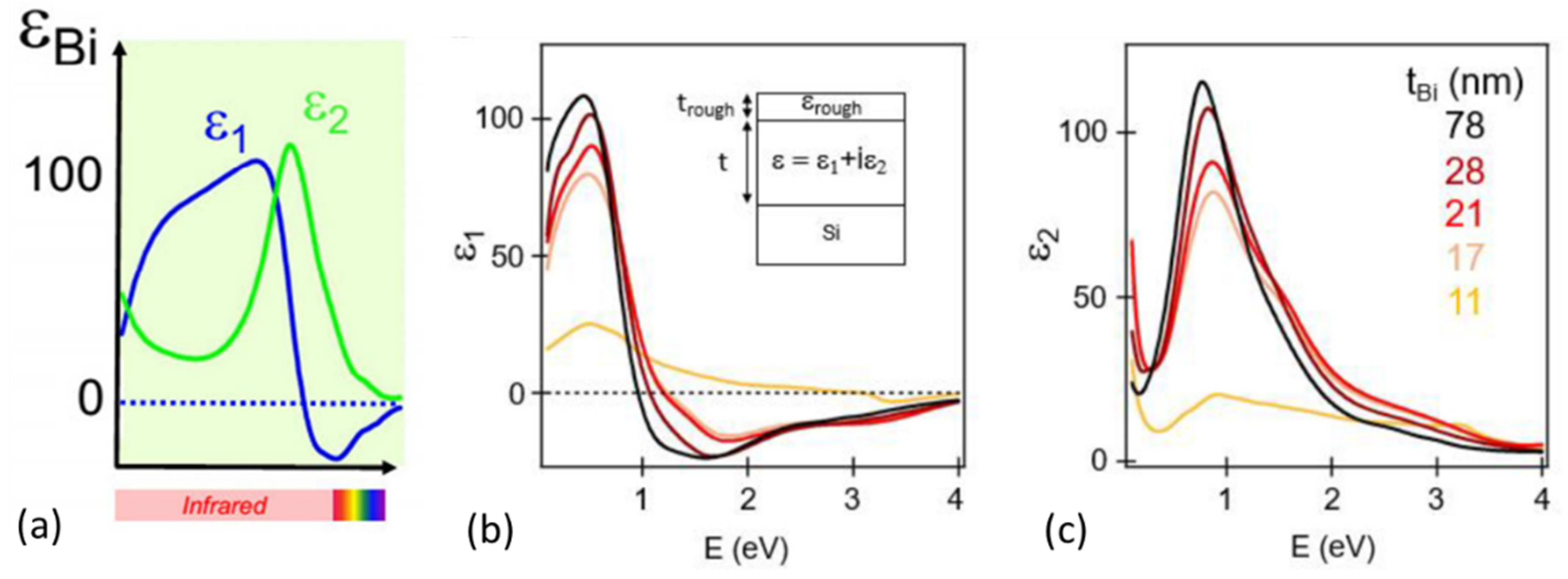
2.2. Optical Dielectric Function of Bismuth
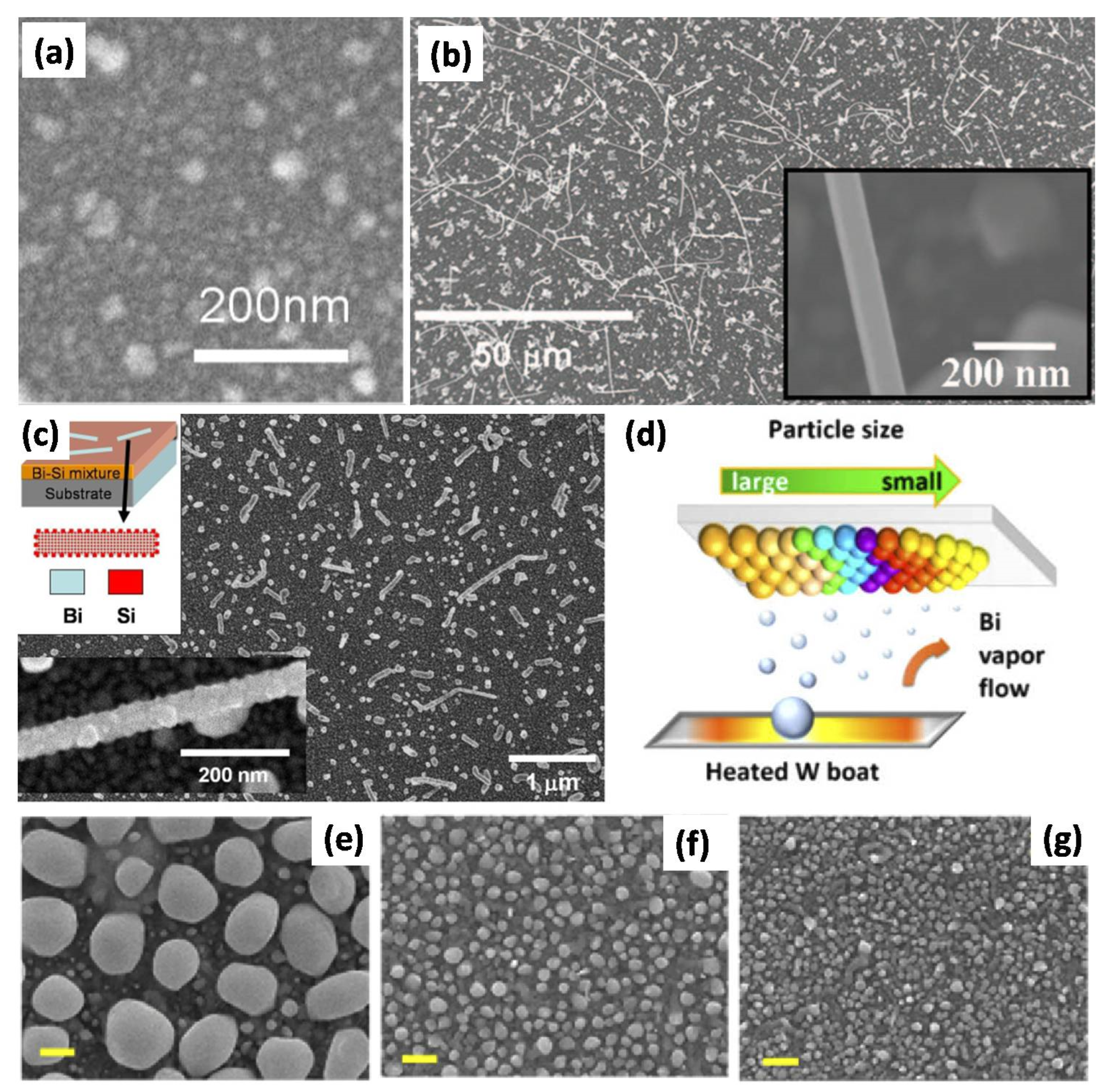
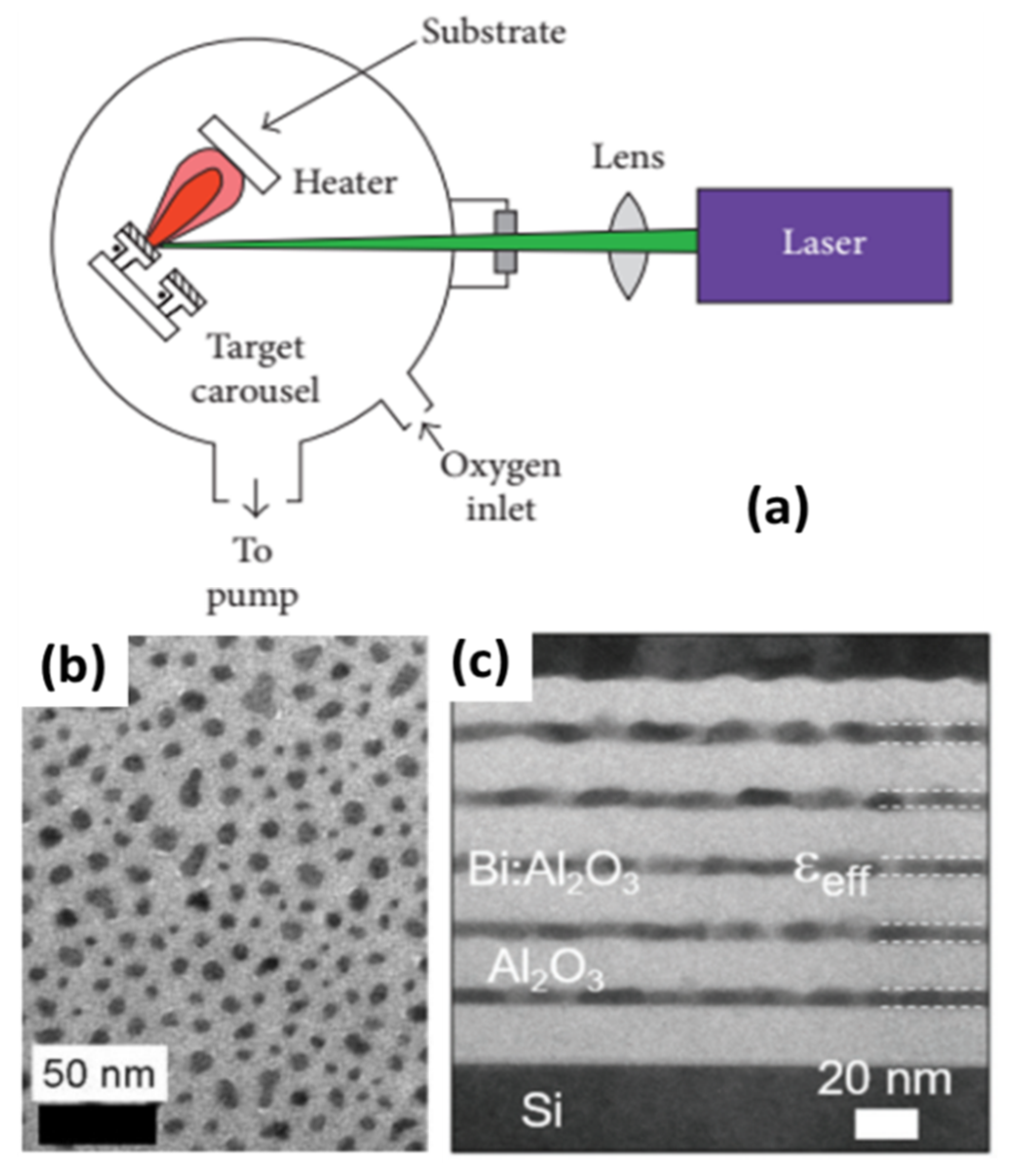
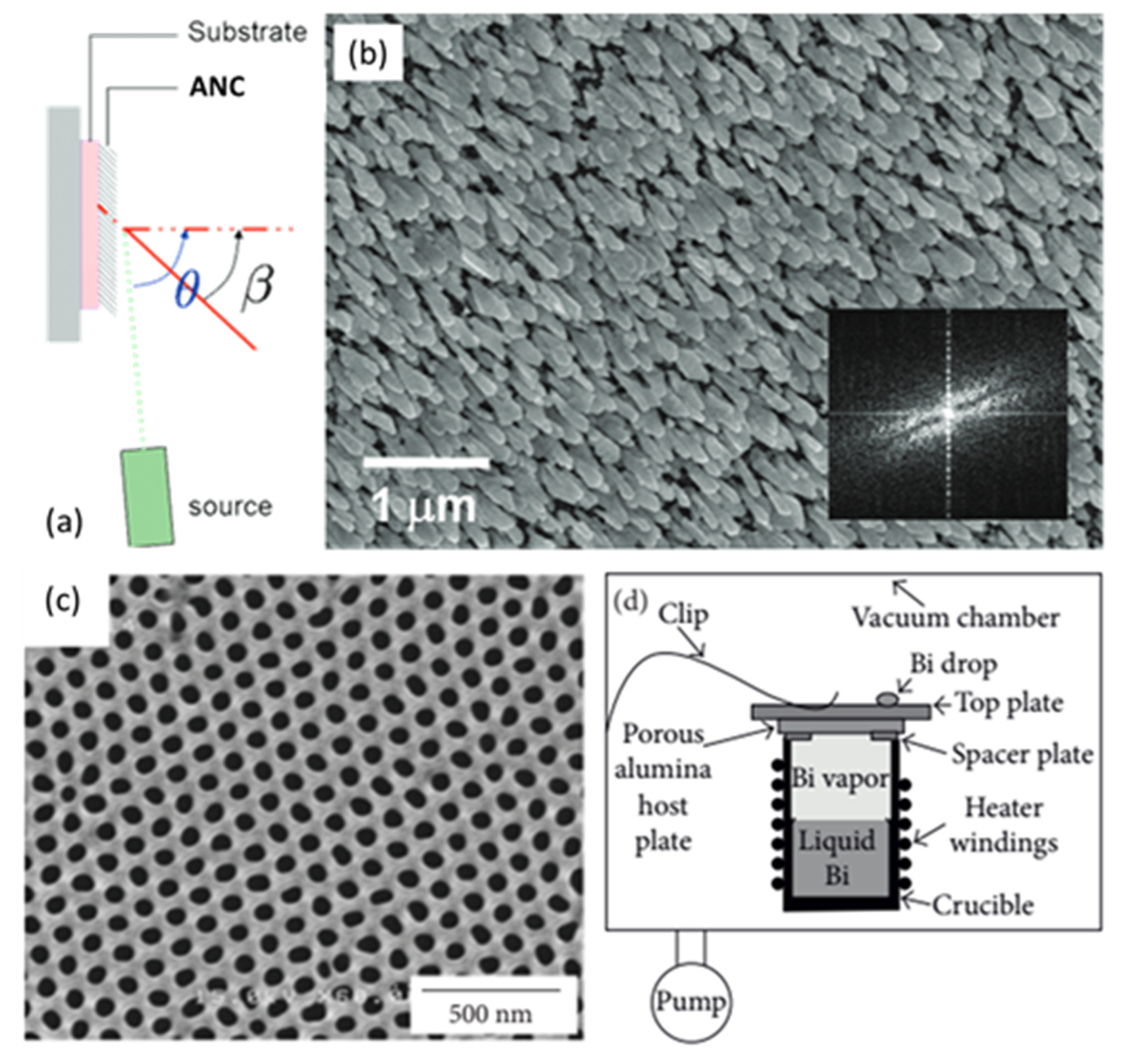
3. Lithography-Free Fabrication of Bismuth Metamaterials
4. Functional Devices Based on Bismuth Metamaterials for Light Manipulation
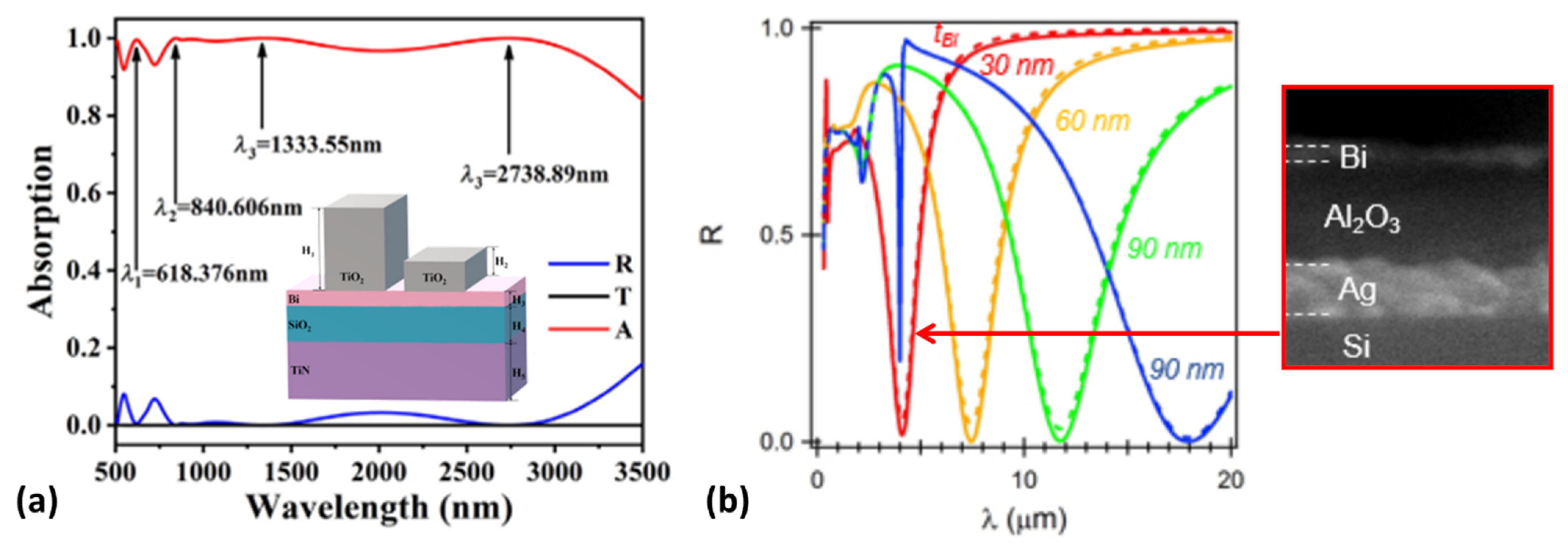
4.1. Light Absorber
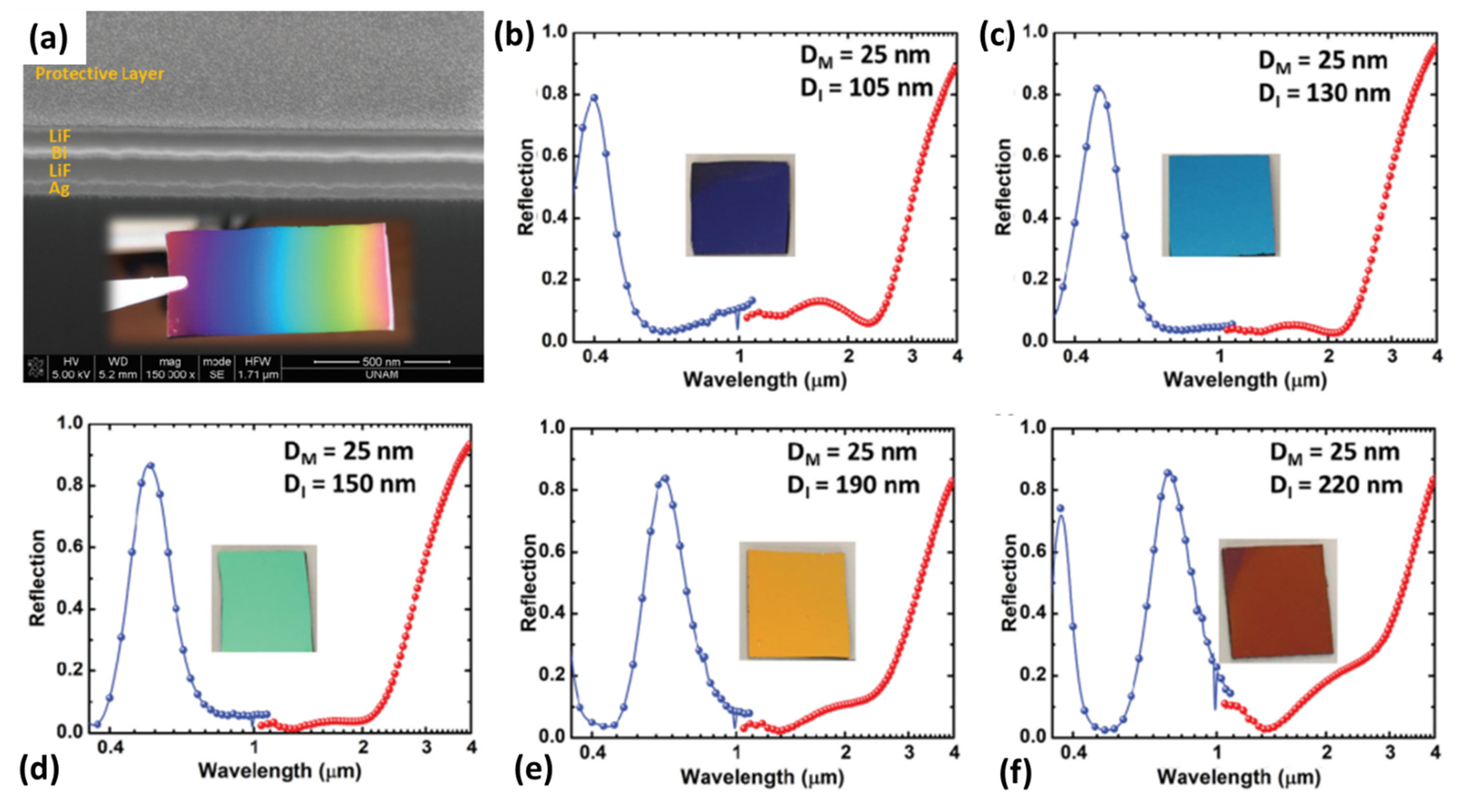
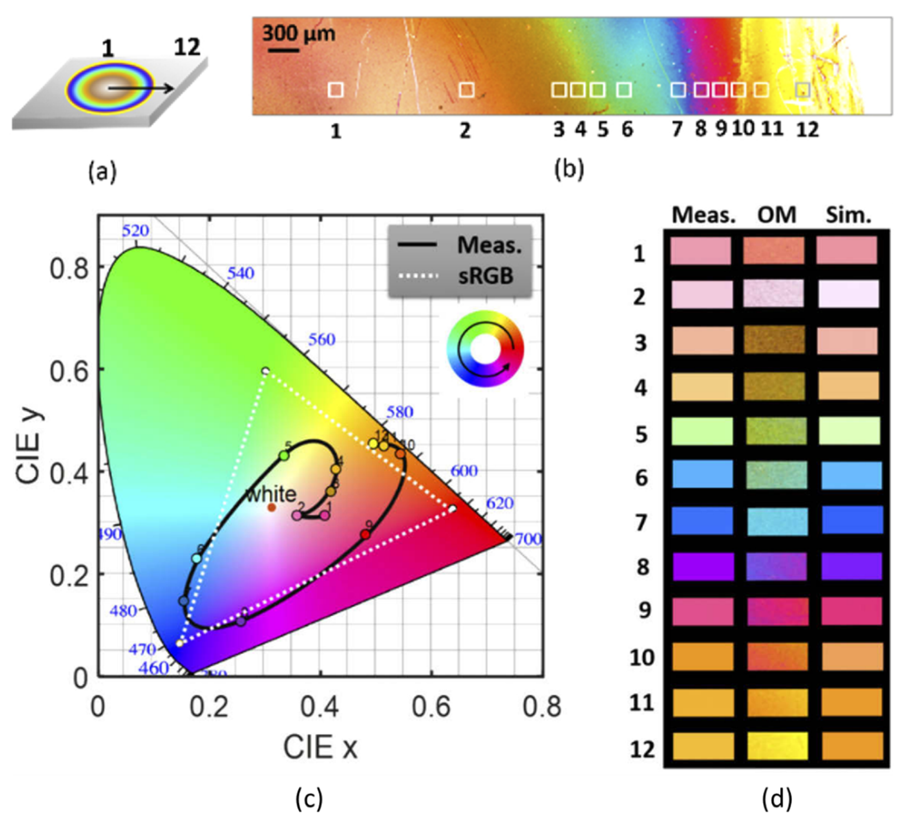
4.2. Color Filter
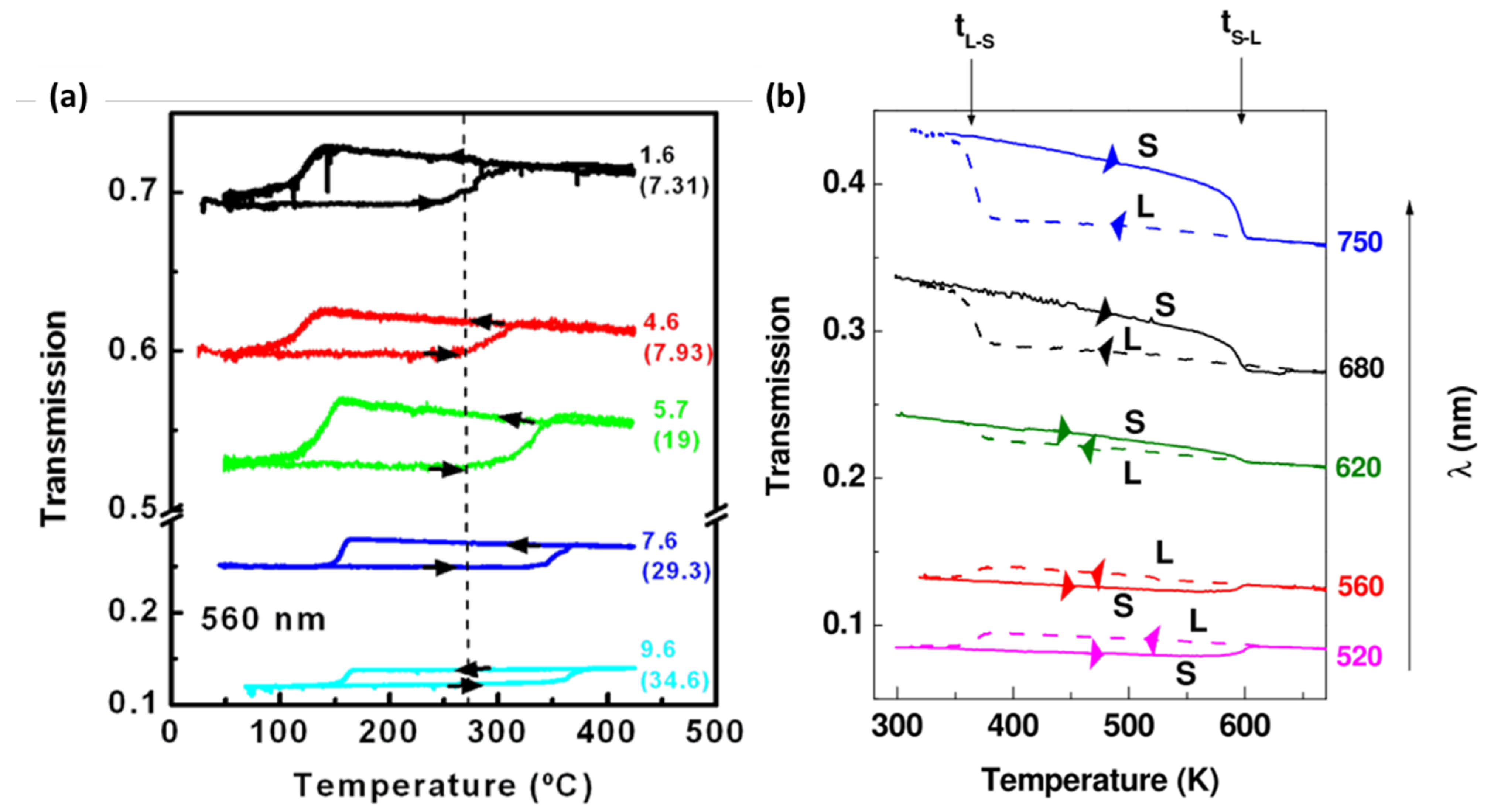
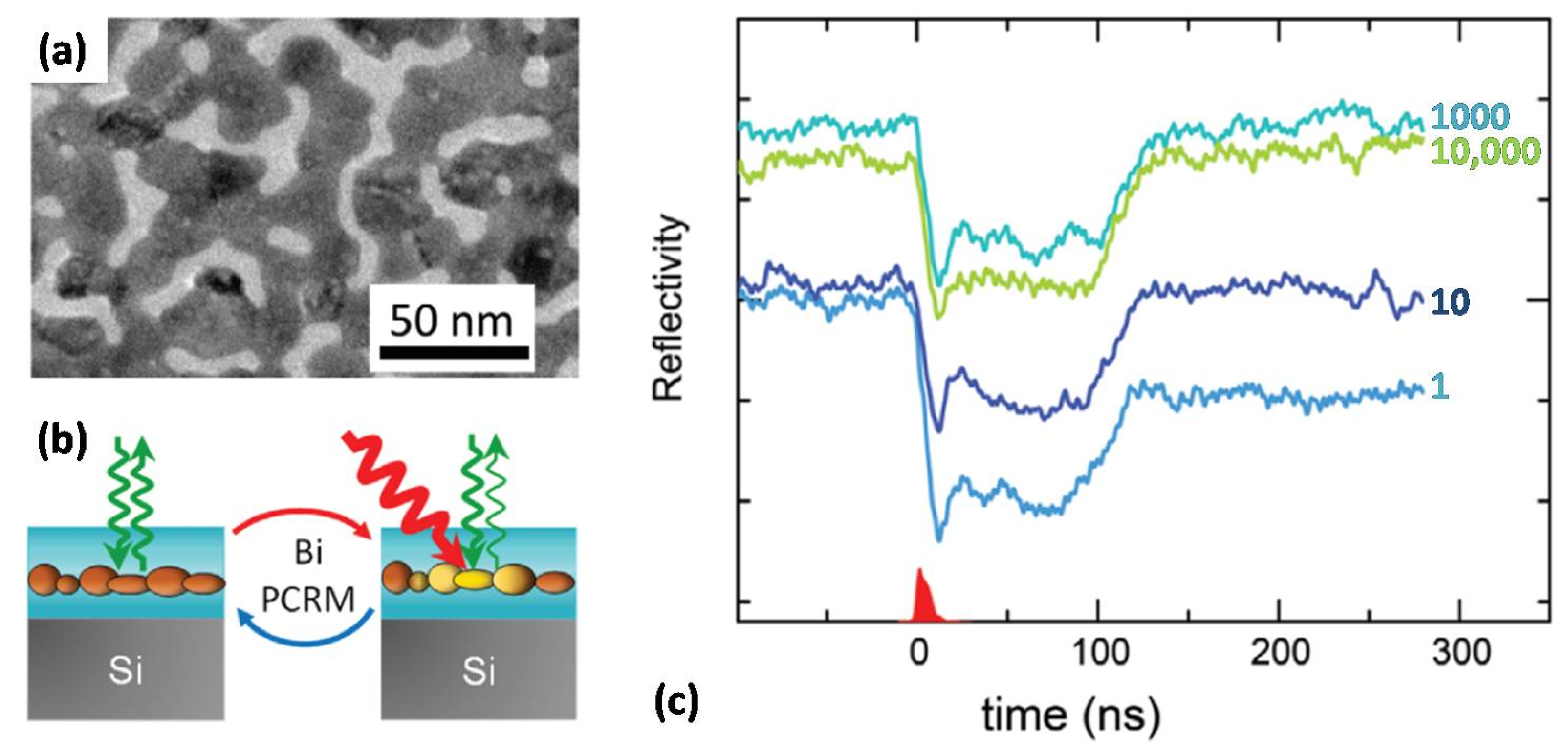
4.3. Thermo-Optical Devices
4.4. Other Applications
5. Conclusions and Perspective
Author Contributions
Funding
Institutional Review Board Statement
Informed Consent Statement
Data Availability Statement
Conflicts of Interest
References
- Liu, Y.; Zhang, X. Metamaterials: A new frontier of science and technology. Chem. Soc. Rev. 2011, 40, 2494–2507. [Google Scholar] [CrossRef]
- Turpin, J.P.; Bossard, J.A.; Morgan, K.L.; Werner, D.H.; Werner, P.L. Reconfigurable and Tunable Metamaterials: A Review of the Theory and Applications. Int. J. Antennas Propag. 2014, 2014, 429837. [Google Scholar] [CrossRef]
- Li, H.; Zhou, H.; Wei, G.; Xu, H.; Qin, M.; Liu, J.; Wu, F. Photonic spin-selective perfect absorptance on planar metasurfaces driven by chiral quasi-bound states in the continuum. Nanoscale 2023, 15, 6636–6644. [Google Scholar] [CrossRef] [PubMed]
- Yang, K.; Wang, J.; Yao, X.; Lyu, D.; Zhu, J.; Yang, Z.; Ren, B. Large-Area Plasmonic Metamaterial with Thickness-Dependent Absorption. Adv. Opt. Mater. 2021, 9, 2001375. [Google Scholar] [CrossRef]
- Harvey, E.; Ghantasala, M. 12—Nanofabrication. In Nanostructure Control of Materials; Hannink, R.H.J., Hill, A.J., Eds.; Woodhead Publishing: Sawston, UK, 2006; pp. 303–330. [Google Scholar]
- Wang, S.; Zhou, Z.; Li, B.; Wang, C.; Liu, Q. Progresses on new generation laser direct writing technique. Mater. Today Nano 2021, 16, 100142. [Google Scholar] [CrossRef]
- Vazquez-Mena, O.; Gross, L.; Xie, S.; Villanueva, L.G.; Brugger, J. Resistless nanofabrication by stencil lithography: A review. Microelectron. Eng. 2015, 132, 236–254. [Google Scholar] [CrossRef]
- Han, M.; Lee, W.; Lee, S.K.; Lee, S.S. 3D microfabrication with inclined/rotated UV lithography. Sens. Actuators A Phys. 2004, 111, 14–20. [Google Scholar] [CrossRef]
- Groves, T.R.; Pickard, D.; Rafferty, B.; Crosland, N.; Adam, D.; Schubert, G. Maskless electron beam lithography: Prospects, progress, and challenges. Microelectron. Eng. 2002, 61–62, 285–293. [Google Scholar] [CrossRef]
- Ali, M.Y.; Hung, W.; Yongqi, F. A review of focused ion beam sputtering. Int. J. Precis. Eng. Manuf. 2010, 11, 157–170. [Google Scholar] [CrossRef]
- Caruana, A.; Cropper, M.; Stanley, S. Spontaneous growth of bismuth nanowires on a sputter-deposited thin bismuth film. Surf. Coatings Technol. 2015, 271, 8–12. [Google Scholar] [CrossRef]
- Huang, J.; Kim, F.; Tao, A.R.; Connor, S.; Yang, P. Spontaneous formation of nanoparticle stripe patterns through dewetting. Nat. Mater. 2005, 4, 896–900. [Google Scholar] [CrossRef] [PubMed]
- Barranco, A.; Borras, A.; Gonzalez-Elipe, A.R.; Palmero, A. Perspectives on oblique angle deposition of thin films: From fundamentals to devices. Prog. Mater. Sci. 2016, 76, 59–153. [Google Scholar] [CrossRef]
- Wang, S.; Zhang, Y.; Wang, W.; Li, G.; Ma, X.; Li, X.; Zhang, Z.; Qian, Y. Template-assisted synthesis of porous molybdenum dioxide nanofibers and nanospheres by redox etching method. J. Cryst. Growth 2006, 290, 96–102. [Google Scholar] [CrossRef]
- Selimis, A.; Mironov, V.; Farsari, M. Direct laser writing: Principles and materials for scaffold 3D printing. Microelectron. Eng. 2015, 132, 83–89. [Google Scholar] [CrossRef]
- Toudert, J. Spectrally Tailored Light-Matter Interaction in Lithography-Free Functional Nanomaterials. Phys. Status Solidi (a) 2019, 217, 1900677. [Google Scholar] [CrossRef]
- Barnes, W.L.; Dereux, A.; Ebbesen, T.W. Surface plasmon subwavelength optics. Nature 2003, 424, 824–830. [Google Scholar] [CrossRef] [PubMed]
- Yu, W.; Tian, Y.; Zhang, S.; Tan, W. Arbitrary power-splitting-ratio achieved in 1×2 hybrid plasmonic multimode inter-ference device by structure symmetry broken. Optik 2020, 220, 165141. [Google Scholar] [CrossRef]
- Tian, Y.; Zhang, S.; Tan, W. An Ultra-Compact Design of Plasmonic Memristor with Low Loss and High Extinction Effi-ciency Based on Enhanced Interaction between Filament and Concentrated Plasmon. Photonics 2021, 8, 437. [Google Scholar] [CrossRef]
- Campos, A.; Troc, N.; Cottancin, E.; Pellarin, M.; Weissker, H.C.; Lermé, J.; Hillenkamp, M. Plasmonic quantum size effects in silver nanoparticles are dominated by interfaces and local environments. Nat. Phys. 2019, 15, 275–280. [Google Scholar] [CrossRef]
- Tian, Y.; Jiang, L.; Deng, Y.; Deng, S.; Zhang, G.; Zhang, X. Bi-nanorod/Si-nanodot hybrid structure: Surface dewetting induced growth and its tunable surface plasmon resonance. Opt. Mater. Express 2015, 5, 2655–2666. [Google Scholar] [CrossRef]
- Ghobadi, A.; Hajian, H.; Butun, B.; Ozbay, E. Strong Light–Matter Interaction in Lithography-Free Planar Metamaterial Perfect Absorbers. ACS Photon. 2018, 5, 4203–4221. [Google Scholar] [CrossRef]
- Amin, R.; Maiti, R.; Carfano, C.; Ma, Z.; Tahersima, M.H.; Lilach, Y.; Ratnayake, D.; Dalir, H.; Sorger, V.J. 0.52 V mm ITO-based Mach-Zehnder modulator in silicon photonics. APL Photon. 2018, 3, 126104. [Google Scholar] [CrossRef]
- Le, K.Q. ITO-based electro-optical modulator integrated in silicon-on-insulator waveguide using surface plasmon interference. Phys. B Condens. Matter. 2021, 602, 412313. [Google Scholar] [CrossRef]
- Guler, U.; Shalaev, V.M.; Boltasseva, A. Nanoparticle plasmonics: Going practical with transition metal nitrides. Mater. Today 2014, 18, 227–237. [Google Scholar] [CrossRef]
- Agarwal, A.; Vitiello, M.S.; Viti, L.; Cupolillo, A.; Politano, A. Plasmonics with two-dimensional semiconductors: From basic research to technological applications. Nanoscale 2018, 10, 8938–8946. [Google Scholar] [CrossRef] [PubMed]
- Ghobadi, A.; Ghobadi, T.G.U.; Ozbay, E. Lithography-free metamaterial absorbers: Opinion. Opt. Mater. Express 2022, 12, 524–532. [Google Scholar] [CrossRef]
- Schindler, F.; Wang, Z.; Vergniory, M.G.; Cook, A.M.; Murani, A.; Sengupta, S.; Kasumov, A.Y.; Deblock, R.; Jeon, S.; Drozdov, I.; et al. Higher-order topology in bismuth. Nat. Phys. 2018, 14, 918–924. [Google Scholar] [CrossRef]
- Huber, T.; Nikolaeva, A.; Gitsu, D.; Konopko, L.; Graf, M. Quantum confinement and surface-state effects in bismuth nanowires. Phys. E: Low-Dimens. Syst. Nanostruct. 2007, 37, 194–199. [Google Scholar] [CrossRef]
- Yang, H.; Fauqué, B.; Malone, L.; Antunes, A.B.; Zhu, Z.; Uher, C.; Behnia, K. Phase diagram of bismuth in the extreme quantum limit. Nat. Commun. 2010, 1, 47. [Google Scholar] [CrossRef]
- Yokota, K.; Takeda, J.; Dang, C.; Han, G.; McCarthy, D.N.; Nagao, T.; Hishita, S.; Kitajima, M.; Katayama, I. Surface metallic states in ultrathin Bi(001) films studied with terahertz time-domain spectroscopy. Appl. Phys. Lett. 2012, 100, 251605. [Google Scholar] [CrossRef]
- Tian, Y.; Toudert, J. Nanobismuth: Fabrication, Optical, and Plasmonic Properties—Emerging Applications. J. Nanotechnol. 2018, 2018, 3250932. [Google Scholar] [CrossRef]
- Shim, W.; Ham, J.; Lee, K.-I.; Jeung, W.Y.; Johnson, M.; Lee, W. On-Film Formation of Bi Nanowires with Extraordinary Electron Mobility. Nano Lett. 2008, 9, 18–22. [Google Scholar] [CrossRef] [PubMed]
- Kim, J.; Shim, W.; Lee, W. Bismuth nanowire thermoelectrics. J. Mater. Chem. C 2015, 3, 11999–12013. [Google Scholar] [CrossRef]
- Yang, F.Y.; Liu, K.; Hong, K.; Reich, D.H.; Searson, P.C.; Chien, C.L. Large Magnetoresistance of Electrodeposited Sin-gle-Crystal Bismuth Thin Films. Science 1999, 284, 1335–1337. [Google Scholar] [CrossRef]
- Huber, T.E.; Celestine, K.; Graf, M.J. Magnetoquantum oscillations and confinement effects in arrays of 270-nm-diameter bismuth nanowires. Phys. Rev. B 2003, 67, 245317. [Google Scholar] [CrossRef]
- Li, L.; Checkelsky, J.G.; Hor, Y.S.; Uher, C.; Hebard, A.F.; Cava, R.J.; Ong, N.P. Phase Transitions of Dirac Electrons in Bismuth. Science 2008, 321, 547–550. [Google Scholar] [CrossRef]
- Liu, Y.; Allen, R.E. Electronic structure of the semimetals Bi and Sb. Phys. Rev. B 1995, 52, 1566–1577. [Google Scholar] [CrossRef]
- Fuseya, Y.; Ogata, M.; Fukuyama, H. Transport Properties and Diamagnetism of Dirac Electrons in Bismuth. J. Phys. Soc. Jpn. 2015, 84, 012001. [Google Scholar] [CrossRef]
- Toudert, J.; Serna, R. Interband transitions in semi-metals, semiconductors, and topological insulators: A new driving force for plasmonics and nanophotonics [Invited]. Opt. Mater. Express 2017, 7, 2299–2325. [Google Scholar] [CrossRef]
- Toudert, J.; Serna, R.; Camps, I.; Wojcik, J.; Mascher, P.; Rebollar, E.; Ezquerra, T.A. Unveiling the Far Infrared-to-Ultraviolet Optical Properties of Bismuth for Applications in Plasmonics and Nanophotonics. J. Phys. Chem. C 2017, 121, 3511–3521. [Google Scholar] [CrossRef]
- Hunderi, O. Optical properties of crystalline and amorphous bismuth films. J. Phys. F: Met. Phys. 1975, 5, 2214. [Google Scholar] [CrossRef]
- Toudert, J.; Serna, R. Ultraviolet-visible interband plasmonics with p-block elements. Opt. Mater. Express 2016, 6, 2434–2447. [Google Scholar] [CrossRef]
- Toudert, J.; Serna, R.; Deeb, C.; Rebollar, E. Optical properties of bismuth nanostructures towards the ultrathin film regime. Opt. Mater. Express 2019, 9, 2924–2936. [Google Scholar] [CrossRef]
- Wang, F.; Fan, H.; Zeng, X. Bismuth-based broadband metamaterial absorber. J. Nanophotonics 2022, 16, 036004. [Google Scholar] [CrossRef]
- Chen, Y.F. Nanofabrication by electron beam lithography and its applications: A review. Microelectron. Eng. 2015, 135, 57–72. [Google Scholar] [CrossRef]
- Wu, J.; Huang, D.; Wu, B.; Wu, X. Extremely broadband light absorption by bismuth-based metamaterials involving hybrid resonances. Phys. Chem. Chem. Phys. 2022, 24, 21612–21616. [Google Scholar] [CrossRef]
- Agarwal, S. Bismuth Based MIM Metamaterial Absorber for Broadband Absorption. In Proceedings of the 2020 6th International Conference on Signal Processing and Communication (ICSC), Noida, India, 5–7 March 2020; pp. 185–187. [Google Scholar]
- Ghobadi, A.; Hajian, H.; Gokbayrak, M.; Butun, B.; Ozbay, E. Bismuth-based metamaterials: From narrowband reflective color filter to extremely broadband near perfect absorber. Nanophotonics 2019, 8, 823–832. [Google Scholar] [CrossRef]
- Toudert, J.; Serna, R.; Pardo, M.G.; Ramos, N.; Peláez, R.J.; Maté, B. Mid-to-far infrared tunable perfect absorption by a sub—λ/100 nanofilm in a fractal phasor resonant cavity. Opt. Express 2018, 26, 34043–34059. [Google Scholar] [CrossRef]
- Xu, Q.; Wen, Z.; Pan, X.; Tan, C.; Zhang, J.; Qiu, Q.; Sun, Y.; Chen, X.; Dai, N.; Chu, J.; et al. Ultra-thin midwavelength infrared absorber using bismuth based planar thin film metamaterials. Appl. Phys. Express 2022, 15, 082005. [Google Scholar] [CrossRef]
- Agarwal, S.; Srivastava, G.; Prajapati, Y.K. Dual band Vis-IR absorber using bismuth based helical metamaterial surface. Opt. Quantum Electron. 2022, 54, 772. [Google Scholar] [CrossRef]
- Su, J.; Mo, X.; Si, G.; Gu, Q.; Jiang, X.; Lv, J. High selectivity color filters based on bismuth enhanced plasmonic nanorods. Opt. Commun. 2021, 490, 126941. [Google Scholar] [CrossRef]
- Cuadrado, A.; Toudert, J.; Serna, R. Polaritonic-to-Plasmonic Transition in Optically Resonant Bismuth Nanospheres for High-Contrast Switchable Ultraviolet Meta-Filters. IEEE Photonics J. 2016, 8, 4801811. [Google Scholar] [CrossRef]
- Garcia-Pardo, M.; Nieto-Pinero, E.; Petford-Long, A.K.; Serna, R.; Toudert, J. Active analog tuning of the phase of light in the visible regime by bismuth-based metamaterials. Nanophotonics 2020, 9, 885–896. [Google Scholar] [CrossRef]
- Alvarez-Alegria, M.; Siegel, J.; Garcia-Pardo, M.; Cabello, F.; Toudert, J.; Haro-Poniatowski, E.; Serna, R. Nanosecond Laser Switching of Phase-Change Random Metasurfaces with Tunable ON-State. Adv. Opt. Mater. 2021, 10, 2101405. [Google Scholar] [CrossRef]
- Soydan, M.C.; Ghobadi, A.; Yildirim, D.U.; Erturk, V.B.; Ozbay, E. Deep Subwavelength Light Confinement in Disordered Bismuth Nanorods as a Linearly Thermal-Tunable Metamaterial. Phys. Status Solidi (RRL)—Rapid Res. Lett. 2020, 14, 2000066. [Google Scholar] [CrossRef]
- de Castro, M.J.; Cabello, F.; Toudert, J.; Serna, R.; Haro-Poniatowski, E. Potential of bismuth nanoparticles embedded in a glass matrix for spectral-selective thermo-optical devices. Appl. Phys. Lett. 2014, 105, 113102. [Google Scholar] [CrossRef]
- de Castro, M.J.; Serna, R.; Toudert, J.; Navarro, J.F.; Haro-Poniatowski, E. Thermo-optical properties of Bi nanoparticles embedded in germanate glasses and alumina thin films. Ceram. Int. 2015, 41, 8216–8222. [Google Scholar] [CrossRef]
- Serna, R.; de Castro, M.J.; Toudert, J.; Haro-Poniatowski, E.; López, J.G. Role of target conditioning on the thermo-optical response of bismuth nanostructures produced by pulsed laser deposition. Appl. Phys. A 2012, 110, 863–867. [Google Scholar] [CrossRef]
- Tian, Y.; Guo, C.F.; Guo, S.; Wang, Y.; Miao, J.; Wang, Q.; Liu, Q. Bismuth nanowire growth under low deposition rate and its ohmic contact free of interface damage. AIP Adv. 2012, 2, 012112. [Google Scholar] [CrossRef]
- Chen, Y.P.; Lai, C.C.; Tsai, W.S. Full-color based on bismuth core-shell nanoparticles in one-step fabrication. Opt. Express 2020, 28, 24511–24525. [Google Scholar] [CrossRef]
- Kumari, L.; Lin, S.-J.; Lin, J.-H.; Ma, Y.-R.; Lee, P.-C.; Liou, Y. Effects of deposition temperature and thickness on the structural properties of thermal evaporated bismuth thin films. Appl. Surf. Sci. 2007, 253, 5931–5938. [Google Scholar] [CrossRef]
- Wu, B.-K.; Lee, H.-Y.; Chern, M.-Y. Bismuth Nanowire Grown Naturally Using a Sputtering System. Appl. Phys. Express 2013, 6, 035504. [Google Scholar] [CrossRef]
- Mihailescu, I.N.; György, E. Pulsed Laser Deposition: An Overview. In International Trends in Optics and Photonics: ICO IV; Asakura, T., Ed.; Springer: Berlin/Heidelberg, Germany, 1999; pp. 201–214. [Google Scholar]
- Tian, Y.; Guo, S.; Liu, Q. Anisotropic nano-column arrays of bismuth and its conductivity. J. Nanosci. Nanotechnol. 2013, 13, 776–780. [Google Scholar] [CrossRef]
- Tian, Y.; Jiang, L.; Zhang, X.; Deng, Y.; Deng, S. Coexistence and competition of surface diffusion and geometric shielding in the growth of 1D bismuth nanostructures and their ohmic contact. Mater. Res. Express 2014, 1, 035034. [Google Scholar] [CrossRef]
- Li, L.; Zhang, Y.; Li, G.; Zhang, L. A route to fabricate single crystalline bismuth nanowire arrays with different diameters. Chem. Phys. Lett. 2003, 378, 244–249. [Google Scholar] [CrossRef]
- Hawkeye, M.M.; Brett, M.J. Glancing angle deposition: Fabrication, properties, and applications of micro- and nanostructured thin films. J. Vac. Sci. Technol. A 2007, 25, 1317–1335. [Google Scholar] [CrossRef]
- Li, H.; Han, P.; Zhang, X.; Li, M. Size-dependent melting point of nanoparticles based on bond number calculation. Mater. Chem. Phys. 2013, 137, 1007–1011. [Google Scholar] [CrossRef]
- Toudert, J. Quantum nanostructures for plasmonics and high refractive index photonics. J. Physics Photon. 2021, 3, 011003. [Google Scholar] [CrossRef]
- Liu, S.; Feng, J.; Tian, Y.; Zhao, H.; Jin, L.; Ouyang, B.; Zhu, J.; Guo, J. Thermo-optic phase shifters based on silicon-on-insulator platform: State-of-the-art and a review. Front. Optoelectron. 2022, 15, 9. [Google Scholar] [CrossRef]
- Tian, Y.; Zhao, Y.; Liu, S.; Li, Q.; Wang, W.; Feng, J.; Guo, J. Scalable and compact photonic neural chip with low learn-ing-capability-loss. Nanophotonics 2022, 11, 329–344. [Google Scholar] [CrossRef]
- Yao, J.D.; Shao, J.M.; Yang, G.W. Ultra-broadband and high-responsive photodetectors based on bismuth film at room temperature. Sci. Rep. 2015, 5, 12320. [Google Scholar] [CrossRef]
- Yao, J.; Zheng, Z.; Shao, J.; Yang, G. Promoting Photosensitivity and Detectivity of the Bi/Si Heterojunction Photodetector by Inserting a WS2 Layer. ACS Appl. Mater. Interfaces 2015, 7, 26701–26708. [Google Scholar] [CrossRef] [PubMed]
- Huber, T.E.; Johnson, S.D.; Belk, J.H.; Hunt, J.H.; Shirvani, K. Charge Transfer and Photocurrent in Interfacial Junctions between Bismuth and Graphene. Phys. Rev. Appl. 2018, 10, 044020. [Google Scholar] [CrossRef]
- Hoffman, C.A.; Meyer, J.R.; Bartoli, F.J.; Di Venere, A.; Yi, X.J.; Hou, C.L.; Wang, H.C.; Ketterson, J.B.; Wong, G.K. Semimetal-to-semiconductor transition in bismuth thin films. Phys. Rev. B 1993, 48, 11431–11434. [Google Scholar] [CrossRef] [PubMed]
- Zhou, G.; Li, L.; Li, G.H. Semimetal to semiconductor transition and thermoelectric properties of bismuth nanotubes. J. Appl. Phys. 2011, 109, 114311. [Google Scholar] [CrossRef]
- Kockert, M.; Mitdank, R.; Moon, H.; Kim, J.; Mogilatenko, A.; Moosavi, S.H.; Kroener, M.; Woias, P.; Lee, W.; Fischer, S.F. Semimetal to semiconductor transition in Bi/TiO2 core/shell nanowires. Nanoscale Adv. 2020, 3, 263–271. [Google Scholar] [CrossRef]
- Wu, B.-K.; Chern, M.-Y.; Lee, H.-Y. Size-controllable synthesis and bandgap modulation of single-layered RF-sputtered bismuth nanoparticles. Nanoscale Res. Lett. 2014, 9, 249. [Google Scholar] [CrossRef]
- Jiang, N.; Su, D.; Spence, J.C.; Zhou, S.; Qiu, J. Volume plasmon of bismuth nanoparticles. Solid State Commun. 2009, 149, 111–114. [Google Scholar] [CrossRef]


Disclaimer/Publisher’s Note: The statements, opinions and data contained in all publications are solely those of the individual author(s) and contributor(s) and not of MDPI and/or the editor(s). MDPI and/or the editor(s) disclaim responsibility for any injury to people or property resulting from any ideas, methods, instructions or products referred to in the content. |
© 2023 by the authors. Licensee MDPI, Basel, Switzerland. This article is an open access article distributed under the terms and conditions of the Creative Commons Attribution (CC BY) license (https://creativecommons.org/licenses/by/4.0/).
Share and Cite
Zhu, L.; Li, Z.; Tian, Y. Lithography-Free Bismuth Metamaterials for Advanced Light Manipulation. Photonics 2023, 10, 602. https://doi.org/10.3390/photonics10050602
Zhu L, Li Z, Tian Y. Lithography-Free Bismuth Metamaterials for Advanced Light Manipulation. Photonics. 2023; 10(5):602. https://doi.org/10.3390/photonics10050602
Chicago/Turabian StyleZhu, Lijun, Zimin Li, and Ye Tian. 2023. "Lithography-Free Bismuth Metamaterials for Advanced Light Manipulation" Photonics 10, no. 5: 602. https://doi.org/10.3390/photonics10050602