Article

Ultra-Broadband, Compact Arbitrary Ratio Power Splitters Enabled by Adiabatic Sub-Wavelength Grating

1
State Key Laboratory of Functional Materials for Informatics, Shanghai Institute of Microsystem and Information Technology, Chinese Academy of Sciences, Shanghai 200050, China
2
University of Chinese Academy of Sciences, Beijing 100049, China
*
Author to whom correspondence should be addressed.
Photonics 2023, 10(5), 578; https://doi.org/10.3390/photonics10050578
Submission received: 7 April 2023 / Revised: 28 April 2023 / Accepted: 8 May 2023 / Published: 15 May 2023
(This article belongs to the Section Optical Communication and Network)

Abstract

:
An ultra-broadband, compact and CMOS-compatible arbitrary ratio power splitter that is based on a directional coupler is proposed on the silicon-on-insulator (SOI) platform. The proposed device consists of an adiabatic sub-wavelength grating (ASWG) and a conventional directional coupler. The wavelength dependence is greatly reduced by introducing an ASWG in the coupling region of the directional coupler. Simulation results show that our proposed device has an operating bandwidth of 250 nm for arbitrary power splitting ratios, with a transmission power variation of less than 8.5%, covering the wavelength range from 1400 nm to 1650 nm. Meanwhile, the device footprint has been narrowed to less than 46 μm. In addition, the power splitters also exhibit a low excess loss of below 0.24 dB. Our proposed ASWG-assisted power splitters show excellent potential for application in large-scale photonic integrated circuits.

1. Introduction

With the exponential growth of data streams, silicon photonics technology has shown enormous application prospects and economic effects in the fields of datacom and telecom [1,2]. Benefiting from great compatibility with the conventional CMOS process [3], photonic integrated chips (PICs) based on SOI platforms provide many advantages, such as high-speed transmission, large data capacity and easy fabrication. The large refractive index contrast between SOI materials allows us to design silicon photonic devices with a more compact footprint, enabling high-density integration and cost reduction [4,5,6]. In silicon photonic systems, power splitters (PSs) are adopted as a building block for power allocation, based on mode interference or mode evolution [7,8]. PSs underpin essential components in many scenarios, including optical switches [9], modulators [10,11], wavelength division (de-)multiplexers (WDMs) [12,13], optical phase arrays (OPAs) [14,15], optical neural networks (ONNs) [16,17], etc. Based on different principles, there are various methods to realize PSs, such as multimode couplers (MMIs), Y-junctions, directional couplers (DCs), etc. MMIs based on the self-imaging principle are a popular choice for achieving power splitting, owing to their small wavelength dependence and compact footprint. However, these devices tend to suffer a non-negligible power imbalance and an insertion loss compared with other PSs [18,19]. Y-junction couplers are also a common choice of design because of their simple construction and easy fabrication. They offer a minor loss and a compact footprint, as well as allowing for arbitrary power splitting ratios (PSRs). However, the loss caused by mode mismatch cannot be ignored when the branch angle is not sufficiently small [20]. DCs have attracted a lot of attention because of their simple structure and compact footprint. The insertion loss is generally low, but these devices exhibit a high wavelength sensitivity, resulting in a poor operating bandwidth [21]. Based on DCs, different schemes have been proposed to reduce the wavelength dependence, including asymmetric DCs, adiabatic DCs and sub-wavelength grating-based DCs (SWG-DCs). Asymmetric DCs modulate the dispersion by introducing an asymmetric structure in the coupling region, thereby increasing the operational bandwidth. However, the improved bandwidth is limited in this method, and it is difficult to further enhance its performance [22,23]. Adiabatic DCs are based on mode evolution, and they are able to achieve a large operating bandwidth with better robustness to fabrication imperfections. However, the dimensions required to achieve the adiabatic mode evolution for adiabatic DCs are too long for large-scale photonic integration [24,25]. SWG-DCs allow for significant improvements in the bandwidth and footprint by introducing periodic pins in the coupling region to modulate the waveguide refractive index. On the downside, these devices sacrifice some fabrication tolerance [26,27]. As a fundamental optical element with substantial application scope, it is essential to implement PSs with a tradeoff of multiple performance characteristics.
In this paper, we propose an ASWG-assisted DC (ASWG-DC), enabling an arbitrary ratio with an ultra-broad bandwidth, compact dimensions and low loss. By introducing an ASWG in the coupling region, a high wavelength insensitivity can be inherently realized in the operating waveband, benefiting from the adiabatic single-mode evolution. In addition, through tuning the width difference of the pins, we can achieve arbitrary PSRs. Simulation results show that the operating bandwidth of the device reaches 250 nm, with a maximum transmission power fluctuation of 8.5%, covering from 1400 nm to 1650 nm for PSRs of 50%:50%, 60%:40%, 70%:30%, 80%:20% and 90%:10%. Benefiting from the adoption of the SWG, the mode evolution footprint can be reduced significantly to less than 46 μm. The ASWG-based arbitrary ratio power splitters exhibit an excess loss as low as 0.24 dB. In addition, our proposed devices also show an excellent robustness to fabrication imperfections. With multiple performance metrics obtained, our proposed device offers great prospects for applications in high-density PICs.

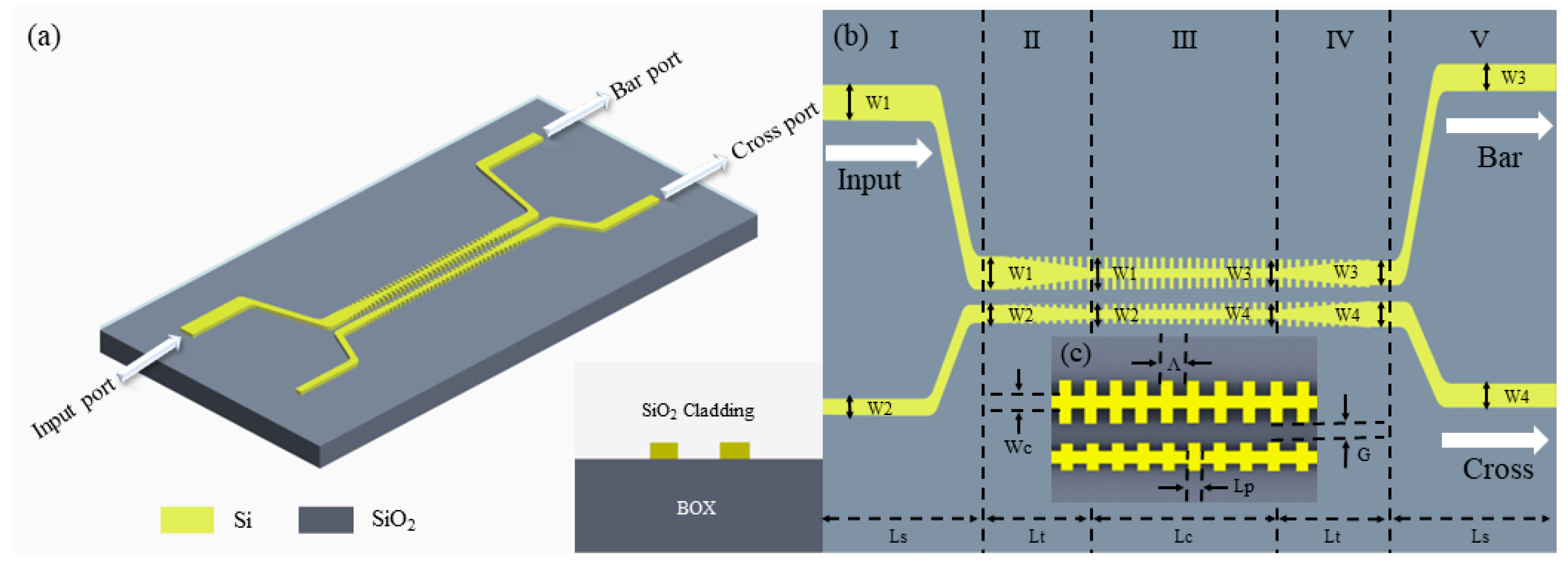
2. Device Schematic and Operation Principle

In a conventional mode-interference-based DC, both the fundamental even and odd modes are initially excited. These two modes interfere with each other, leading to a power oscillation between the two waveguides. Due to the differences in beat length at different wavelengths caused by the mode dispersion, conventional DCs suffer from a large wavelength dependence. In contrast to common DCs, the operating theory of ASWG-DCs is mainly based on the single-mode evolution through the adiabatic transition region. In principle, both the fundamental mode and the next higher-order mode are excited by the excitation of an isolated waveguide mode at the input port. However, provided that the input is sufficiently asynchronous, the power of the isolated mode will mainly merge into a single system mode. This system mode will propagate through the adiabatic transition region with negligible power coupling to the other system mode, given that the structure is sufficiently adiabatic. This behavior ensures that the devices operate in the desired manner for both 3 dB and full couplers and greatly avoids the effect of mode dispersion [28]. Accordingly, ASWG-DCs are inherently broadband, insensitive to fabrication imperfections and do not require an exact length. Our proposed ASWG-DCs are mainly designed based on the SOI platform, and their structure is shown in Figure 1a.
The device is composed of a 220 nm thick silicon waveguide with a 2 μm BOX and a 2 μm thick silicon substrate. On the top of the silicon layer, a 2 μm thick SiO2 is considered as the cladding layer. As shown in Figure 1b,c, to better explain the structure and working principle of the device, the specific structure of the proposed PSs can be divided into five parts. The first section, with a length of Ls, consists mainly of straight and bent waveguides. This section acts as the input of the device and needs to ensure that the input mode from the left port can meet stable single-mode transmissions. Meanwhile, the curved waveguide follows a Bessel curve. Since the trend of the waveguide changes slowly, the loss of the waveguide can be further reduced. The second portion of the device is composed of tapered waveguides with a length of Lt and a pair of SWGs with the same pins. The widths of the trapezoid structures are tapered from W1 and W2 to Wc, with the widths of the upper and lower SWGs remaining W1 and W2, respectively. In designing this part of the structure, it is necessary to ensure that the light field does not convert into higher-order modes when propagating in this region. Region III consists of two strip waveguides with lengths of Lc and widths of Wc, separated by G, and adiabatic sub-wavelength gratings. The pins of the upper and lower gratings are tapered from W1, W2 to W3, W4, respectively, allowing the mode evolution as the light enters the region. The coupling strength is also enhanced with the ASWG introduced, making the footprint for mode evolution significantly narrower. Conventional adiabatic evolution devices usually require lengths of more than 100 μm to maintain single-mode propagation, which is not conducive to large-scale photonic integration. In addition, we can adjust the refractive index of the waveguide to control the power distribution of the incident optical field. Specifically, arbitrary PSRs can be achieved by optimizing the width of the pins and the width of the strip waveguide, Wc. Region IV mainly contains trapezoid waveguides with lengths of Lt and SWGs with widths of W3 and W4. The widths of the trapezoid waveguides are tapered from Wc to W3 and W4, respectively. Region V, with a length of Ls, has a similar structure to Region I, allowing the decoupled modes to propagate out stably. It is designed to connect the ASWG-DC with the rest of the photonic integrated circuits. Both Region IV and Region V need to be designed to ensure that the optical modes do not convert to higher-order modes. In addition, although the widths of the SWGs in the different regions are not fixed, they all have an identical variation period of Λ, and the lengths of the pins are all Lp, with the upper and lower pins separated by G. Based on the above design principles, we initially set the SWG length Lc in the coupling region to 20 μm and the widths W1, W2, W3 and W4 to 610 nm, 350 nm, 480 nm and 480 nm. Moreover, we chose 200 nm as the variation period Λ, and the pins’ length Lp was set to 100 nm [29]. The detailed parameter settings are shown in Table 1.
As mentioned above, based on the mode evolution principle, the refractive index can be modulated by adjusting the structure of the pair of ASWGs and the widths of the core straight-strip waveguides in the adiabatic transition region, thereby changing the allocation of the optical field at the emitting end. We defined the width difference ∆W1 at the right end of the SWGs in region III as:
W 1 = W 3 W 4
As shown in Figure 2, based on the parameter settings in Table 1, we simulated the optical transmission at the cross port at 1550 nm when changing the lower SWG widths of W2 and W4. In the simulation process, we kept W3 at 480 nm and varied W4 from 440 nm to 480 nm to modify ΔW1. In addition, we needed to keep the gap of the pair of ASWGs constant. As a result, W2 and W4 had to be changed for the lower ASWG with the waveguide taper angle constant when the width difference ΔW1 was introduced. We initially employed the mature commercial software Lumerical Eigenmode Expansion (EME) to calculate the function of the power splitting ratio of the adiabatic coupler and ΔW1, with the transverse electric (TE) fundamental mode being excited at the input. The EME solver can be used to address Maxwell’s equations in the frequency domain by, firstly, slicing the device along the main propagation axis and then solving for the eigenmodes in each cell. A 20 nm mesh grid was adopted in the simulation, and the perfect match layer (PML) was used in three different dimensions. Based on the optimized results, the Lumerical 3D finite-difference time-domain (FDTD) was used for further verification of the arbitrary power splitting performance. The FDTD solver is able to divide the simulation model into discrete time and volume grid-constructed cells and further solve the corresponding Maxwell’s equations to obtain the required field components.
It was clear that as ΔW1 varied from 0 to 40 nm, the transmission from the bar port could vary from 0 to 0.5. Based on this principle, arbitrary PSRs can theoretically be achieved. The coupling strength of conventional directional couplers is known to be strongly wavelength-dependent and, thus, has a narrow operating bandwidth. By introducing an ASWG in the coupling region, we were able to significantly attenuate the impact of dispersion, increase the operating bandwidth and decrease the footprint. Moreover, the adiabatic length does not need to be precisely defined due to the single-mode evolution, which leaves room for further reduction in the adiabatic evolution length under different power splitting ratios. For high-density silicon photonic systems, our proposed device offers a promising application scope that profits from the multiple performance metrics.

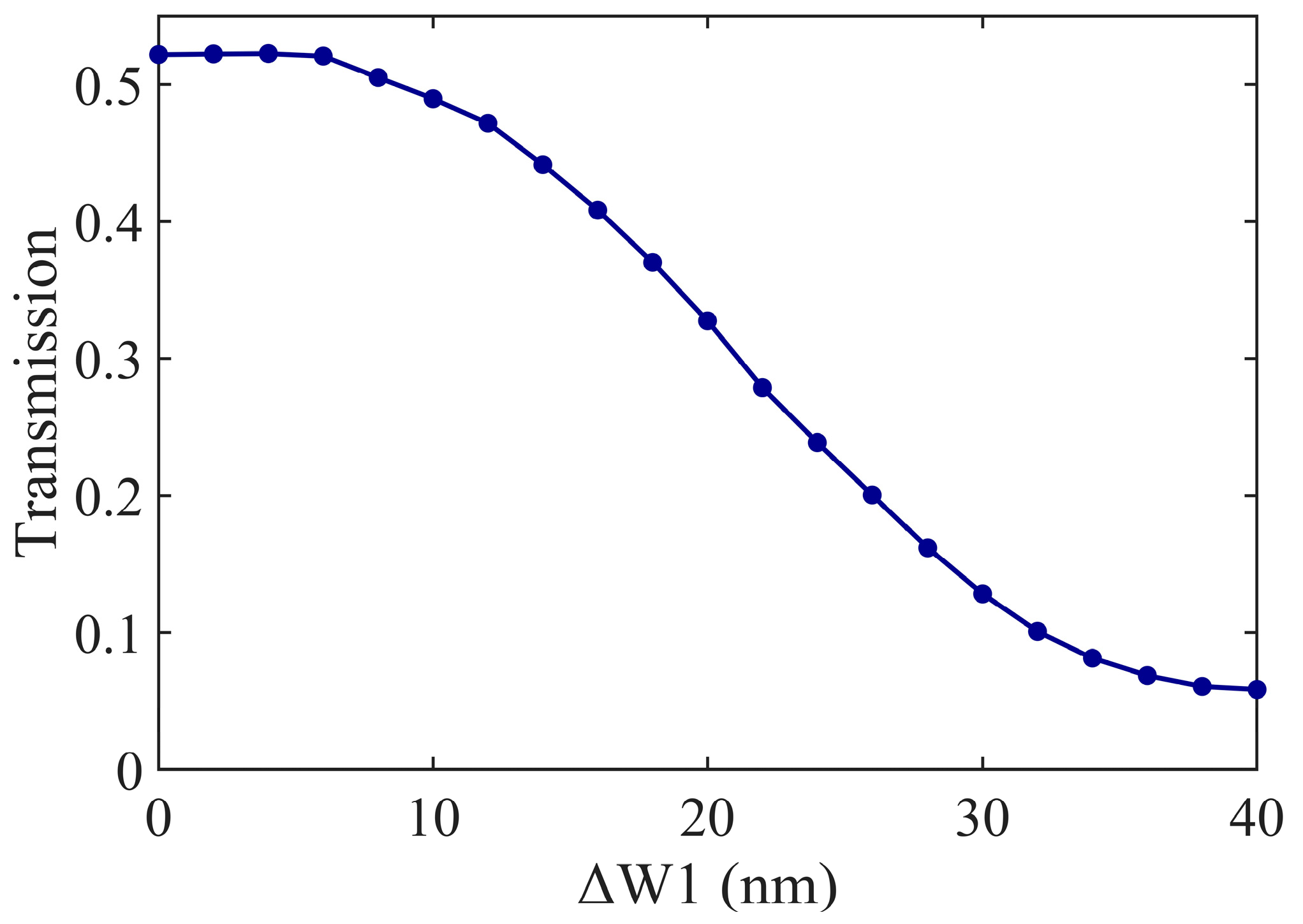
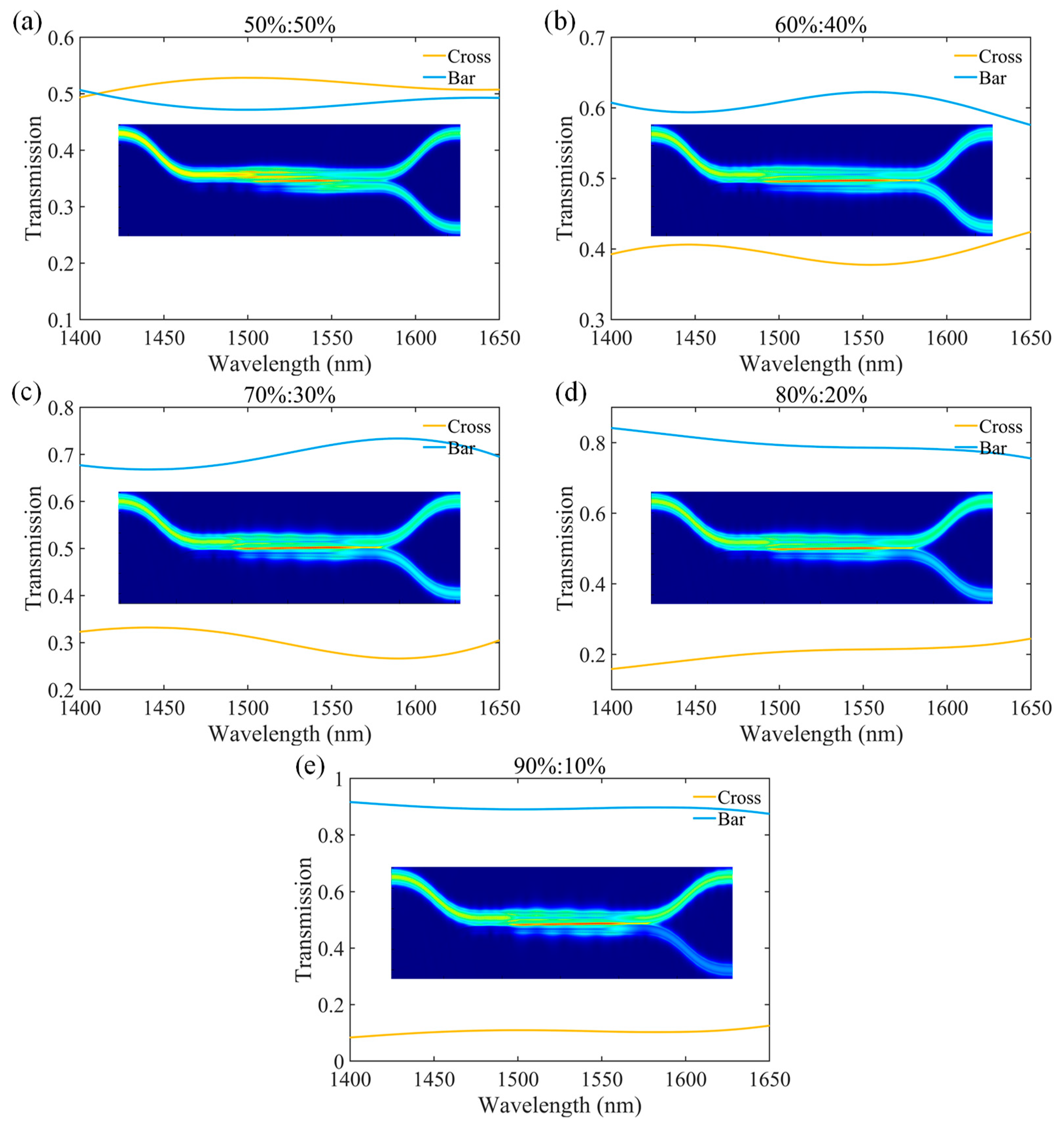
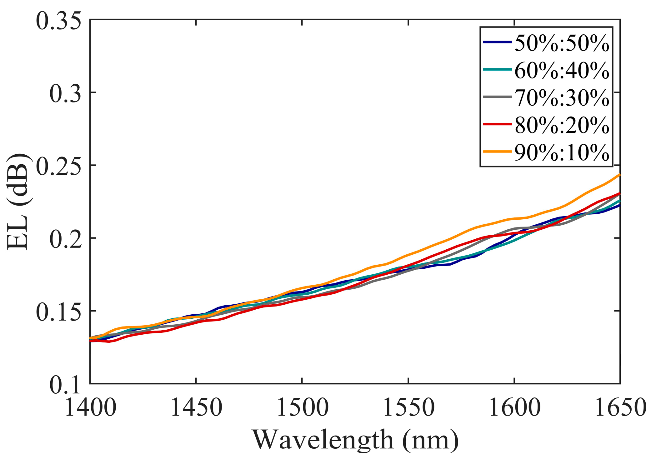
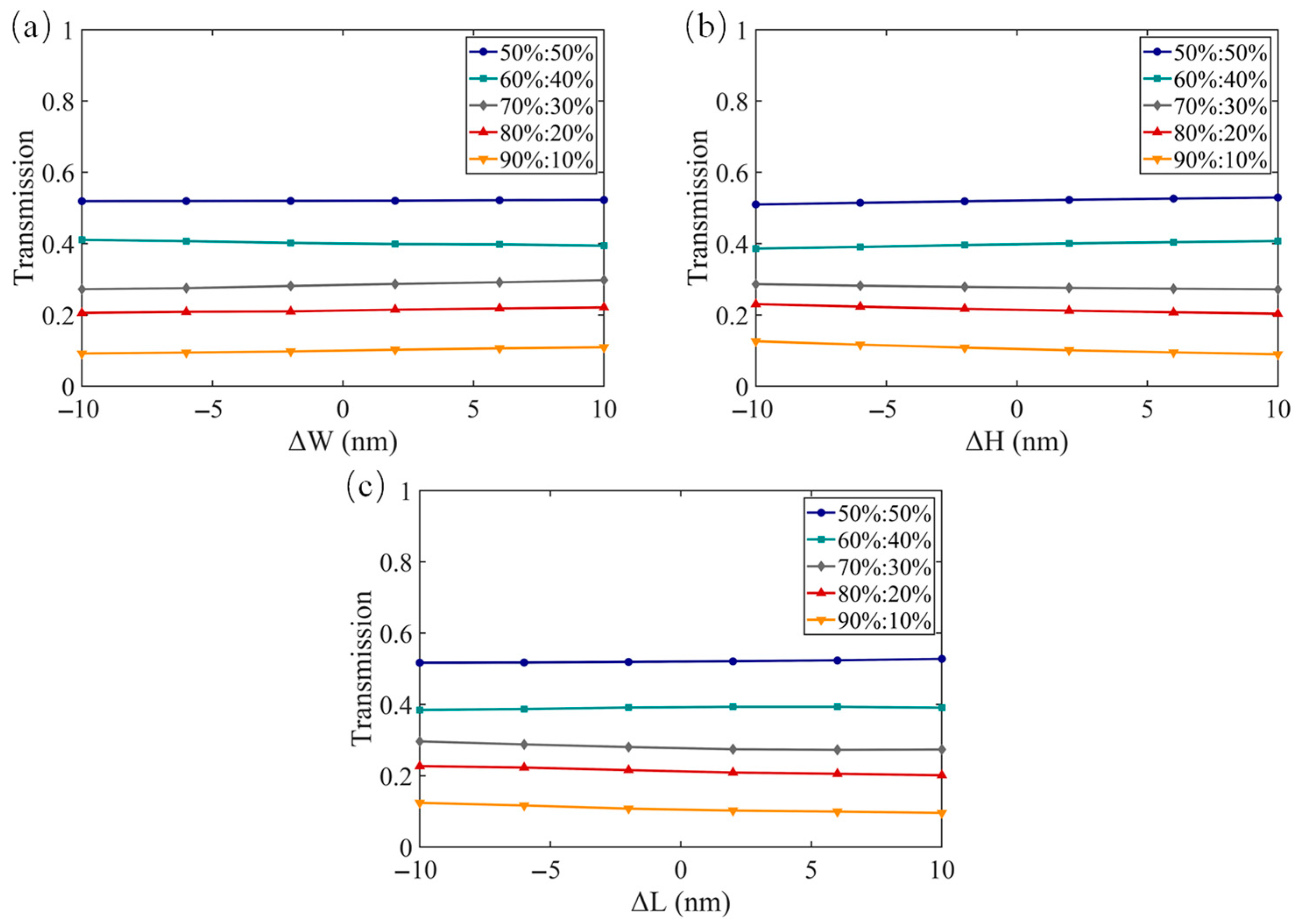
3. Results and Discussion

In the optimization process, we simulated the complete device through the mature commercial software Lumerical 3D FDTD, with the TE fundamental modes as excitation and the light source covering wavelengths from 1400 nm to 1650 nm. To verify that the proposed structure could realize arbitrary PSRs, we simulated structural variations in the SWG-DCs to optimize the device performance for PSRs of 50%:50%, 60%:40%, 70%:30%, 80%:20% and 90%:10%. The 4.1 Ghz Core-i7 CPU was employed, and 160 GB RAM was provided for the computing resources. In the simulation process, the mesh grid was set to 20 nm, and the boundary conditions for different dimensions were perfectly matched layers, with each simulation taking about 5 h. We defined the PSR at the two outputs of the device as follows:
P S R = T c r o s s / ( T b a r + T c r o s s )
where Tbar represents the transmission obtained from bar port, and Tcross stands for the transmission obtained from cross port. As shown in Figure 3, when the TE mode was incident from input port, we simulated the transmission curve for arbitrary PSRs and corresponding light field profiles.
According to the simulation results, our optimized device can perform reliable power splitting in the desired operating waveband, with a minor wavelength dependence, given maximum transmission power variations of 3.5%, 4.6%, 6.6%, 8.5% and 4.7% from the bar port for splitting ratios from 50%:50% to 90%:10%. After the light is incident from the input port, it undergoes mode evolution in the coupling region and exits steadily from the bar port and the cross port without conversion to higher-order modes. Conventional SWG-based devices are designed based on the mode interference principle and involve different modes which suffer from the birefringence. Our proposed power splitters are designed based on the principle of adiabatic mode evolution. By designing the SWG as a trapezoidal shape, perfect adiabatic evolution can be achieved at a sufficient length. This maintains a stable, single-mode propagation and avoids the desired mode converting into other modes, effectively realizing birefringence-free operation. The structural parameters corresponding to the PSRs from 50%:50% to 90%:10% are shown in Table 2, based on our optimization data. The adiabatic evolution principle can also be applied to TM mode operations, but the parameters for the corresponding arbitrary power splitting ratios need to be redesigned based on the characteristics of the TM mode.
Due to the refractive index modulation of the SWG, the dimensions of the adiabatic gratings for arbitrary power splitting ratios were drastically reduced to below 16 μm, with a total footprint of less than 46 μm. In addition, we calculated the excess loss (EL) of the device in the wavelength range from 1400 nm to 1650 nm. We defined the EL of the device as follows:
E L = 10 log 10 T b a r + T c r o s s
As shown in Figure 4, the EL of our proposed device is as low as 0.24 dB. This shows that our device is capable of achieving ultra-broad bandwidth, compact size and low loss simultaneously, providing a relatively comprehensive performance improvement.
In subsequent device fabrication processes, our proposed device will be fabricated on a commercial SOI wafer from Soitec. We will process the designed waveguide pattern through employing electron beam lithography (EBL), with a positive resist for zep 250 nm being used as the photomask. There is only one etch required because our device is designed based on a strip waveguide with a silicon layer thickness of 220 nm. The top layer of silicon will be fully etched to a depth of 220 nm via inductively coupled plasma (ICP) dry etching to yield the complete waveguide structure. Prior to device fabrication, it is essential that the robustness of the proposed device to fabrication imperfections be investigated accordingly. The transmission from the bar port at a wavelength of 1550 nm was simulated when the waveguide thickness varied from −10 nm to 10 nm, the width varied from −10 nm to 10 nm and the width of the pins varied from −10 nm to 10 nm. When we changed the thickness of the waveguides, the other structural parameters remained at their original values, and vice versa. As shown in Figure 5, it is clear that the devices are able to operate steadily within the above fabrication deviation levels.
The comparison of the simulation results between the state-of-the-art imbalanced couplers and the ASWG-DCs demonstrated in this work is summarized in Table 3. To the best of our knowledge, our proposed adiabatic evolution-based power splitters offer a much smaller footprint compared to other adiabatic couplers, as well as an ultra-broad operating bandwidth covering the E, S, C, L and U wavebands. With multiple performance metrics, our study provides a significant potential for application in the large-scale silicon system.

4. Conclusions

In conclusion, we present an ASWG-assisted arbitrary ratio PS with ultra-broad bandwidth, a compact footprint and low loss. By optimizing the structure of the ASWG to tune the refractive index, the wavelength dependence and dimensions of the device can be significantly improved. Through FDTD simulations, we realized PSRs from 50%:50% to 90%:10% with an operating bandwidth of 250 nm, covering 1400 to 1650 nm. In the operating waveband above, our proposed device exhibits stable power splitting characteristics, with transmission power fluctuations of less than 8.5% for arbitrary power splitting ratios. Benefiting from the introduction of the SWGs, the device dimensions were reduced to less than 46 μm. In addition, our work shows that the excess loss of the device is below 0.24 dB. It was also found that the device offers significant robustness to fabrication imperfections. With a tradeoff of multiple performance metrics, our proposed device shows great potential for applications in large-scale PICs.

Author Contributions

Conceptualization, X.L., Z.S. and F.G.; methodology, X.L. and Y.Z.; software, X.L.; validation, X.L.; formal analysis, X.L.; investigation, X.L.; resources, X.L.; data curation, X.L.; writing—original draft preparation, X.L.; writing—review and editing, Y.Z. and X.L.; visualization, X.L.; supervision, Y.Z. All authors have read and agreed to the published version of the manuscript.

Funding

This work was funded by the National Key Research and Development Program of China [2022YFB2803100]; the National Major Scientific Research Instrument Development Project [22127901]; and the Shanghai Sailing Program [22YF1456700].

Institutional Review Board Statement

Not applicable.

Informed Consent Statement

Not applicable.

Data Availability Statement

Relevant data are available from the authors upon reasonable request.

Conflicts of Interest

The authors declare no conflict of interest.

References

  1. Pitris, S.; Moralis-Pegios, M.; Alexoudi, T.; Ban, Y.; De Heyn, P.; Van Campenhout, J.; Lambrecht, J.; Ramon, H.; Yin, X.; Bauwelinck, J.; et al. O-Band Silicon Photonic Transmitters for Datacom and Computercom Interconnects. J. Light. Technol. 2019, 37, 5140–5148. [Google Scholar] [CrossRef]
  2. Shi, Y.; Zhang, Y.; Wan, Y.; Yu, Y.; Zhang, Y.; Hu, X.; Xiao, X.; Xu, H.; Pan, B. Silicon photonics for high-capacity data communications. Photon. Res. 2022, 10, A106–A134. [Google Scholar] [CrossRef]
  3. Li, H.; Casper, B.; Balamurugan, G.; Sakib, M.; Sun, J.; Driscoll, J.; Kumar, R.; Jayatilleka, H.; Rong, H.; Jaussi, J. A 112 Gb/s PAM4 Silicon Photonics Transmitter With Microring Modulator and CMOS Driver. J. Light. Technol. 2020, 38, 131–138. [Google Scholar] [CrossRef]
  4. Ferrotti, T.; Chantre, A.; Blampey, B.; Duprez, H.; Milesi, F.; Myko, A.; Sciancalepore, C.; Hassan, K.; Harduin, J.; Baudot, C.; et al. Power-efficient carrier-depletion SOI Mach-Zehnder modulators for 4x25Gbit/s operation in the O-band. In Silicon Photonics X; SPIE: Bellingham, WA, USA, 2015. [Google Scholar]
  5. Stojanović, V.; Ram, R.J.; Popović, M.; Lin, S.; Moazeni, S.; Wade, M.; Sun, C.; Alloatti, L.; Atabaki, A.; Pavanello, F.; et al. Monolithic silicon-photonic platforms in state-of-the-art CMOS SOI processes [Invited]. Opt. Express 2018, 26, 13106–13121. [Google Scholar] [CrossRef]
  6. Giewont, K.; Hu, S.; Peng, B.; Rakowski, M.; Rauch, S.; Rosenberg, J.C.; Sahin, A.; Stobert, I.; Stricker, A.; Nummy, K.; et al. 300-Mm Monolithic Silicon Photonics Foundry Technology. IEEE J. Sel. Top. Quantum Electron. 2019, 25, 1–11. [Google Scholar] [CrossRef]
  7. Gupta, R.K.; Chandran, S.; Das, B.K. Wavelength-Independent Directional Couplers for Integrated Silicon Photonics. J. Light. Technol. 2017, 35, 4916–4923. [Google Scholar] [CrossRef]
  8. Peter, E.; Thomas, A.; Dhawan, A.; Sarangi, S.R. Active microring based tunable optical power splitters. Opt. Commun. 2016, 359, 311–315. [Google Scholar] [CrossRef]
  9. Chen, S.; Shi, Y.; He, S.; Dai, D. Low-Loss and Broadband 2 × 2 Silicon Thermo-Optic Mach–Zehnder Switch with Bent Directional Couplers. Opt. Lett. 2016, 41, 836–839. [Google Scholar] [CrossRef]
  10. Jain, S.; Rajput, S.; Kaushik, V.; Kumar, M. High speed optical modulator based on silicon slotted-rib waveguide. Opt. Commun. 2019, 434, 49–53. [Google Scholar] [CrossRef]
  11. Barrios, C.; de Almeida, V.; Lipson, M. Low-power-consumption short-length and high-modulation-depth silicon electrooptic modulator. J. Light. Technol. 2003, 21, 1089–1098. [Google Scholar] [CrossRef]
  12. Horst, F.; Green, W.M.; Assefa, S.; Shank, S.M.; Vlasov, Y.A.; Offrein, B.J. Cascaded Mach-Zehnder wavelength filters in silicon photonics for low loss and flat pass-band WDM (de-)multiplexing. Opt. Express 2013, 21, 11652–11658. [Google Scholar] [CrossRef] [PubMed]
  13. Feng, C.; Ying, Z.; Zhao, Z.; Gu, J.; Pan, D.Z.; Chen, R.T. Wavelength-division-multiplexing (WDM)-based integrated electronic–photonic switching network (EPSN) for high-speed data processing and transportation. Nanophotonics 2020, 9, 4579–4588. [Google Scholar] [CrossRef]
  14. Poulton, C.V.; Yaacobi, A.; Cole, D.B.; Byrd, M.J.; Raval, M.; Vermeulen, D.; Watts, M.R. Coherent solid-state LIDAR with silicon photonic optical phased arrays. Opt. Lett. 2017, 42, 4091–4094. [Google Scholar] [CrossRef] [PubMed]
  15. Poulton, C.V.; Byrd, M.J.; Russo, P.; Timurdogan, E.; Khandaker, M.; Vermeulen, D.; Watts, M.R. Long-Range LiDAR and Free-Space Data Communication With High-Performance Optical Phased Arrays. IEEE J. Sel. Top. Quantum Electron. 2019, 25, 1–8. [Google Scholar] [CrossRef]
  16. Totovic, A.; Giamougiannis, G.; Tsakyridis, A.; Lazovsky, D.; Pleros, N. Programmable photonic neural networks combining WDM with coherent linear optics. Sci. Rep. 2022, 12, 5605. [Google Scholar] [CrossRef]
  17. Moralis-Pegios, M.; Mourgias-Alexandris, G.; Tsakyridis, A.; Giamougiannis, G.; Totovic, A.; Dabos, G.; Passalis, N.; Kirtas, M.; Rutirawut, T.; Gardes, F.Y.; et al. Neuromorphic Silicon Photonics and Hardware-Aware Deep Learning for High-Speed Inference. J. Light. Technol. 2022, 40, 3243–3254. [Google Scholar] [CrossRef]
  18. Han, L.; Kuo, B.P.-P.; Alic, N.; Radic, S. Ultra-broadband multimode 3dB optical power splitter using an adiabatic coupler and a Y-branch. Opt. Express 2018, 26, 14800–14809. [Google Scholar] [CrossRef]
  19. Chen, W.; Lin, J.; Li, H.; Wang, P.; Dai, S.; Liu, Y.; Yao, R.; Li, J.; Fu, Q.; Dai, T.; et al. Broadband multimode 3 dB optical power splitter using tapered couplers. Opt. Express 2022, 30, 46236. [Google Scholar] [CrossRef]
  20. Hu, M.; Huang, J.; Scarmozzino, R.; Levy, M.; Osgood, R. A low-loss and compact waveguide Y-branch using refractive-index tapering. IEEE Photon. Technol. Lett. 1997, 9, 203–205. [Google Scholar] [CrossRef]
  21. Kim, H.; Shin, H. Tailorable and Broadband On-Chip Optical Power Splitter. Appl. Sci. 2019, 9, 4239. [Google Scholar] [CrossRef]
  22. Lu, Z.; Yun, H.; Wang, Y.; Chen, Z.; Zhang, F.; Jaeger, N.A.F.; Chrostowski, L. Broadband silicon photonic directional coupler using asymmetric-waveguide based phase control. Opt. Express 2015, 23, 3795–3808. [Google Scholar] [CrossRef] [PubMed]
  23. Wu, Y.; Chiang, K.S. Ultra-broadband mode multiplexers based on three-dimensional asymmetric waveguide branches. Opt. Lett. 2017, 42, 407–410. [Google Scholar] [CrossRef] [PubMed]
  24. Zhu, J.; Chao, Q.; Huang, H.; Zhao, Y.; Li, Y.; Tao, L.; She, X.; Liao, H.; Huang, R.; Zhu, Z.; et al. Compact, broadband, and low-loss silicon photonic arbitrary ratio power splitter using adiabatic taper. Appl. Opt. 2021, 60, 413–416. [Google Scholar] [CrossRef] [PubMed]
  25. Mao, D.; Alam, S.; Zhang, J.; Zhu, M.; Koh, P.-C.; Plant, D.V.; Wang, Y.; El-Fiky, E.; Xu, L.; Kumar, A.; et al. Adiabatic Coupler With Design-Intended Splitting Ratio. J. Light. Technol. 2019, 37, 6147–6155. [Google Scholar] [CrossRef]
  26. Xu, L.; Wang, Y.; Kumar, A.; El-Fiky, E.; Mao, D.; Tamazin, H.; Jacques, M.; Xing, Z.; Saber, G.; Plant, D.V. Compact high-performance adiabatic 3-dB coupler enabled by subwavelength grating slot in the silicon-on-insulator platform. Opt. Express 2018, 26, 29873–29885. [Google Scholar] [CrossRef]
  27. Zhao, S.; Liu, W.; Chen, J.; Ding, Z.; Shi, Y. Broadband Arbitrary Ratio Power Splitters Based on Directional Couplers With Subwavelength Structure. IEEE Photon. Technol. Lett. 2021, 33, 479–482. [Google Scholar] [CrossRef]
  28. Ramadan, T.; Scarmozzino, R.; Osgood, R. Adiabatic couplers: Design rules and optimization. J. Light. Technol. 1998, 16, 277–283. [Google Scholar] [CrossRef]
  29. Yun, H.; Chrostowski, L.; Jaeger, N.A.F. Ultra-broadband 2 × 2 adiabatic 3 dB coupler using subwavelength-grating-assisted silicon-on-insulator strip waveguides. Opt. Lett. 2018, 43, 1935–1938. [Google Scholar] [CrossRef]
  30. Papadovasilakis, M.; Chandran, S.; Gebregiorgis, Y.; Bian, Y.; Rakowski, M.; Krishnamurthy, S.; Aboketaf, A.; Augur, R.; Viegas, J. Fabrication tolerant and wavelength independent arbitrary power splitters on a monolithic silicon photonics platform. Opt. Express 2022, 30, 33780–33791. [Google Scholar] [CrossRef]
Figure 1. (a) Schematic view of the proposed ASWG-DC on a SOI platform. (b) The top view of the schematic and the geometric parameters of the device. (c) A zoom-in of the schematic and geometric parameters of the ASWG.
Photonics 10 00578 g001
Figure 2. The simulated transmission from cross port at wavelength of 1550 nm, given W 1 varying from 0 to 40 nm.
Photonics 10 00578 g002
Figure 3. Simulated transmission curves and corresponding electric field profiles of arbitrary splitting ratio power splitters: (a) 50%:50%; (b) 60%:40%; (c) 70%:30%; (d) 80%:20%; and (e) 90%:10%.
Photonics 10 00578 g003
Figure 4. The calculated EL of ASWG-DCs for arbitrary PSRs from 1400 nm to 1650 nm.
Photonics 10 00578 g004
Figure 5. Simulated fabrication tolerance of ASWG-DCs for arbitrary splitting ratios. (a) Strip waveguide width deviation of ΔW with waveguide thickness remaining at 220 nm and pin lengths remaining at 100 nm; (b) Strip waveguide thickness deviation ΔH with waveguide widths remaining unchanged and pin lengths remaining at 100 nm; (c) Pin length deviation of ΔL with waveguide widths remaining unchanged and thickness remaining at 220 nm.
Photonics 10 00578 g005
Table 1. Parameters and corresponding values of the proposed device.
SymbolValueSymbolValue
Wc0.12 μmLt15 μm
W10.61 μmLc20 μm
W20.35 μmLp0.1 μm
W30.48 μmΛ0.2 μm
W40.48 μmG0.1 μm
Ls10 μm
Table 2. Parameters and characteristics for different SRs.
Splitting RatioW4 (nm)Lc (μm)Wc (nm)
50%:50%48011115
60%:40%47316115
70%:30%46615105
80%:20%45714110
90%:10%44414115
Table 3. Comparison of simulation results of the reported power splitter and this work.
ReferenceTypeSize (μm)Operation BandBandwidth (nm)EL (dB)
[26]SWG, Adiabatic DC65S + C + L100<0.2
[25]Adiabatic DC240O200NA
[24]Adiabatic DC80S + C + L1000.05
[19]MMI52.5S + C + L100<1.5
[30]Asymmetric DC60O80<0.38
This workASWG, DC46E + S + C + L + U250<0.24
Disclaimer/Publisher’s Note: The statements, opinions and data contained in all publications are solely those of the individual author(s) and contributor(s) and not of MDPI and/or the editor(s). MDPI and/or the editor(s) disclaim responsibility for any injury to people or property resulting from any ideas, methods, instructions or products referred to in the content.

