Communication

Room–Temperature Terahertz Detector Based on Monolayer Graphene Integrated with an Asymmetric Bowtie Antenna

1
State Key Laboratory of Optoelectronic Materials and Technologies, Guangdong Province Key Laboratory of Display Material and Technology, Sun Yat-sen University, Guangzhou 510275, China
2
School of Electronics and Information Technology, Sun Yat-sen University, Guangzhou 510275, China
*
Authors to whom correspondence should be addressed.
These authors contributed equally to this work.
Photonics 2023, 10(5), 576; https://doi.org/10.3390/photonics10050576
Submission received: 3 April 2023 / Revised: 23 April 2023 / Accepted: 7 May 2023 / Published: 15 May 2023
(This article belongs to the Special Issue Micro-Nano Optical Devices)

Abstract

:
Terahertz (THz) technology has great potential for applications in various fields, such as security imaging detection, optical communication, environmental quality monitoring, and life sciences. Most of these applications require THz detectors with high sensitivity, fast response, and a miniaturized size that can operate at room temperature. In this study, we present a graphene THz detector integrated with an asymmetric bowtie antenna. The asymmetric antenna confines the incident THz waves into the graphene active layer, leading to photocurrent generation and its directional flow. The maximum responsivity of this device can reach 19.6 V/W at 2.52 THz, with a noise–equivalent power (NEP) of 0.59 nW /Hz0.5. Additionally, the response time is less than 21 μs, with an active area of less than 1500 μm2. Such a small device enables THz imaging with a spatial resolution as small as 200 μm. These results provide a feasible way to design miniaturized and integrable two–dimensional material–based THz detectors.

1. Introduction

Terahertz (THz) waves are electromagnetic waves in the frequency range between 0.1 THz and 10 THz, which exhibit unique features such as strong penetration, low photon energy, and large bandwidth compared to microwaves. These characteristics make THz science and technology play an increasingly important role in various fields, including security imaging detection, environmental quality monitoring, medical and health diagnosis, information communication, national defense security, and astronomy [1,2,3,4,5]. Most of these applications require detectors with high sensitivity, fast response, room temperature operation, and miniaturized array integration.
The majority of room–temperature terahertz detectors are based on bulk materials and utilize thermal detection [6,7,8,9]. However, traditional thermal detectors suffer from slow response times and low sensitivity, which limits their practical applications. Although electronic detectors, such as complementary metal–oxide–semiconductor (CMOS)–based field effect transistors (FET) and Schottky barrier diodes, have fast response times, their detection efficiency is usually low at high frequencies because they usually do not have dedicated antennae designed at higher frequencies. This makes their broadband and high–frequency detection a challenge [10,11,12]. As a result, these detectors based on bulk materials have limited applicability. Emerging two–dimensional (2D) materials have numerous advantages, including high mobility, strong configurability, flexibility, transparency, and easy integration, making them ideal for terahertz wave detection [13,14,15]. Among the most representative and attractive of these materials is graphene, which possesses many extraordinary properties, including high carrier mobility, tunable charge carriers by electrostatic gating, and excellent chemical stability. Additionally, graphene exhibits a linear Dirac dispersion relationship, resulting in a gapless spectrum and massless Dirac fermions [16]. This unique characteristic allows graphene to have a broadband absorption spectrum, ranging from the visible to the GHz–THz range, making it one of the most favorable 2D photoactive materials for terahertz detection.
In 2012, researchers first utilized graphene for terahertz wave detection by taking advantage of its high electron mobility. The high electron mobility of the 2D Dirac electrons in graphene allows it to support weakly damped plasma wave oscillations upon THz illumination, enabling a fast photoresponse at room temperature [17]. Over the past few years, numerous studies have been conducted on graphene–based photodetection in the THz range, which can be classified into three detection categories: bolometric effect, plasma wave resonance effect, and photo–thermoelectric effect [18,19,20,21]. In particular, the photo–thermoelectric effect relies on photocurrent generation due to the difference in THz wave absorption in graphene regions next to the two metallic electrodes. Such a different electromagnetic absorption can generate a temperature gradient and, thereafter, the non–equilibrium distributions of the energetic electrons, giving to net current via the thermoelectric effect. In comparison to the former two detection mechanisms, the photo–thermoelectric effect is more favorable for room–temperature THz detection in terms of its fast response (up to picosecond) [22], high sensitivity, and broad operation frequency range.
Currently, the photo–thermoelectric detection of graphene is achieved by contacting the graphene layer with dissimilar metals [23], placing the monolayer graphene stripe in a departure from the center of a square–spiral antenna [24], and integrating the graphene layer to asymmetric THz antenna [21]. In comparison to the former two architectures, the asymmetric THz antenna can concentrate the incident THz wave and enhance the electromagnetic absorption in the graphene layer. Furthermore, the asymmetric antenna will lead to different absorption of the THz wave across the graphene layer. Such difference can give rise to a temperature gradient across the graphene channel and generate photocurrent flow via the photo–thermoelectric effect. These features can guarantee a high sensitivity of the detectors. Therefore, the utilization of graphene and other 2D materials for THz detection based on the photo–thermoelectric effect highlights the crucial need for an efficient and easily integrable asymmetric antenna, especially for the on–chip integration of these detectors.
In the current study, we present a graphene–based detector integrated with an asymmetric bowtie antenna for room temperature THz detection and imaging utilizing the photo–thermoelectric effect. By utilization of the designed asymmetric bowtie metal antenna, we achieve nonuniform THz wave absorption within the graphene monolayer, whereby a high responsivity of 19.6 V/W and a fast response of 20 μs can be obtained from the detector. Compared to traditional antennas that achieve asymmetry of the source and gate through symmetric designs such as the symmetrical logarithmic periodic antenna [17], bow tie antenna [21], etc., with the drain being led out elsewhere, we have developed an alternative approach that eliminates the need for a gate. By directly carving out one side of the bowtie antenna, we achieve asymmetric source–drain enhancement, greatly simplifying the antenna’s design and fabrication process. Furthermore, we show that such a detector can be employed for raster scanning imaging. Due to the small footprint of the detector, a spatial resolution as small as 200 μm can be achieved. These results, therefore, demonstrate a facile approach for the design and fabrication of room–temperature 2D THz miniaturized detectors with high sensitivity and fast response.

2. Experimental Section

2.1. Design of Asymmetric THz Antenna

The asymmetric THz antenna is schematically illustrated in Figure 1A, which was designed using the high–frequency structure simulator (HFSS) software. The antenna was placed on a 500 μm thick intrinsic silicon substrate coated with a layer of 300 nm SiO2. The antenna layer consists of 10 nm Ti and 100 nm Au, with the Ti layer directly contacting the substrate. The metal layers were set as a perfect electrical conductor (PEC) during simulation in the THz spectral regime. To determine the size range of the antenna, we calculated the effective wavelength, λeff, at the interface, which is determined by the following empirical formula [25],
λ eff = λ / ε eff
where εeff represents the effective dielectric constant of the environment surrounding the antenna, and λ is the free–space wavelength of the incident THz wave. The effective dielectric constant of the interface can be approximated as,
ε eff = ε med + ε air / 2
where εmed denotes the dielectric constant of the Si substrate (11.9), and εair is the dielectric constant of air (=1). The effective wavelength experienced by the antenna at 2.52 THz is then determined as 47 μm.
With this information, we optimized the design of the asymmetric bowtie antenna by conducting parameter sweeps using the Optimetrics module of HFSS.

2.2. Fabrication of Graphene THz Detector Integrated with the Asymmetric Bowtie Antenna

Monolayer graphene was grown using the chemical vapor deposition (CVD) method (Beijing Graphene Institute, China). To fabricate the detector, a graphene monolayer was first transferred onto an intrinsic silicon wafer (with a resistivity ρ > 20,000 Ω·cm) coated with a 300 nm thick SiO2 layer. The graphene was then patterned using maskless lithography (UPG501, Wavetest, Germany) and etched in an oxygen plasma environment. The asymmetric antenna was then patterned and deposited onto the graphene by electron–beam evaporation (DE400, Wavetest), which consisted of titanium (10 nm thickness) and gold (100 nm thickness) layers. Finally, the obtained device was annealed in an Ar/H2 mixture (150 sccm/350 sccm) at 450 °C for 90 min to make better contact between the graphene and metal electrode.

2.3. Characterizations

Raman spectra were acquired utilizing a micro–Raman spectrometer (inVia Reflex, Renishaw, UK). The samples were irradiated with an excitation laser with a wavelength of 532 nm, which was focused onto the samples using a 50× objective with a numerical aperture of 0.80. The diameter of the focal spot was approximately 1 μm. Two–dimensional Raman mapping was obtained by scanning the sample below the laser spot at a step size of 0.1 μm. The integration time for collecting each spectrum is 0.2 s. Scanning electron microscopy (SEM) images were obtained using an SEM instrument (FEI Quanta450, FEI, USA). The thickness of the graphene flakes was measured using an atomic force microscope (AFM, NTEGRA Spectra, NT–MDT, Russia).
The fabricated detector was bonded to a printed circuit board to establish contact and facilitate electrical measurements. The electrical transport properties of the detector were measured using a source meter (Keithley 2636B, Tektronix, USA). For photocurrent characterizations, the THz wave (FIRL–100, Edinburgh Instruments, UK) was modulated by a chopper and directed toward the detector. The output frequency is 2.52 THz. The detector, in turn, generated a photocurrent signal at the same frequency as the chopper’s modulation frequency. This photocurrent signal was captured using a transimpedance current amplifier (DLPCA–200, Femto, Germany) without bias and connected to a lock–in amplifier (SR830, Stanford Research, USA). The photocurrent can be calculated via I p h = 2 π 2 L / 4 G , where L represents the lock–in signal, and 2 π 2 / 4 accounts for peak–to–peak amplitude, root–mean–square amplitude of the lock–in amplifier and sine wave Fourier component of the square wave generated by the chopper. G is the transimpedance of the pre–amplifier, which is set as 106 V/A. The modulation frequency was tunable from 100 Hz to 7.5 kHz. The power of the THz wave was calibrated using a commercial pyroelectric detector (AC2500–H, Scientech, USA). To investigate the polarization dependence of the photocurrent, we systematically rotated the device while keeping the incident THz wave linearly polarized in a fixed direction. For raster scanning imaging using the detector, we collimated the THz wave using gold–coated 90° off–axis parabolic mirrors. The collimated wave was then focused onto the sample at an incident angle of 0 degrees. To facilitate scanning, we mounted the sample holder on a 2D linear motorized stage, which was precisely controlled by the system software.
All experiments were conducted in ambient conditions at room temperature.

3. Results and Discussion

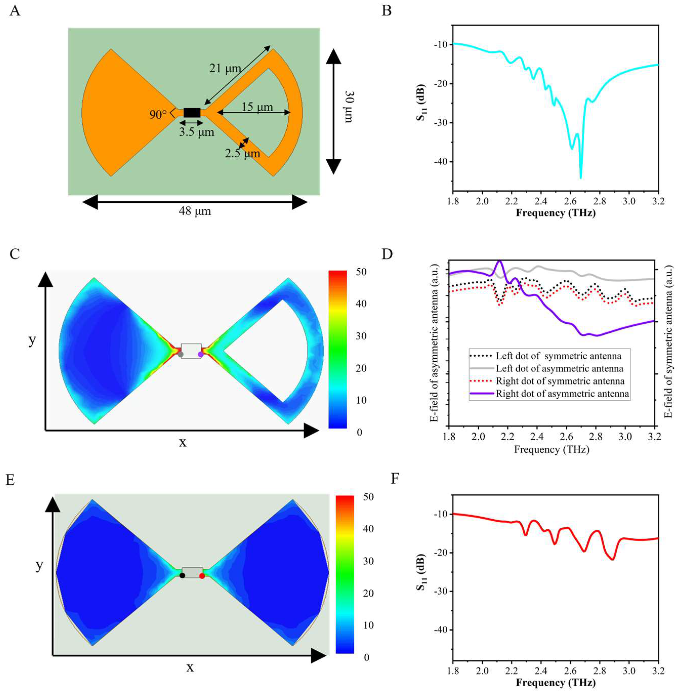
The goal of the design of the antenna is to improve the radiation efficiency and increase the difference in the electric field within the channel. According to the output frequency of the THz source used in our current study (see Section 2.3), the target operating frequency of the antenna is 2.52 THz. As shown in Figure 1A, the asymmetrical antenna we designed is based on a bowtie–shaped antenna, where the left lobe is solid, and the right lobe is hollow. The radii of the two bowties are both 21 μm. The opening angles are 90°. The length of the channel region between the two lobes, where the graphene monolayer will be integrated, is set as L = 3.5 μm (Figure 1A).
According to the simulated return loss (S11) shown in Figure 1B, which indicates the antenna’s radiation efficiency, the antenna displays a low return loss (less than −20 dB) within the relatively narrow frequency range of 2.4 THz to 2.8 THz. This satisfies the design requirements for higher radiation efficiency at 2.52 THz. The photo–thermoelectric effect response depends on the temperature difference induced by the asymmetric absorption of the left and right sides of the channel, which is determined by the in–plane electric field amplitude distributions. In Figure 1C, the in–plane electric field distributions coupled by the antenna at 2.52 THz are revealed through HFSS simulation. The electric field amplitudes on the left side of the channel are much different from those on the right side. Specific values of the in–plane electric field were collected from 1.8 THz to 3.2 THz at the purple and gray dots marked on both sides of the channel. As shown in Figure 1D, the electric field on the left side fluctuates around 1.4 × 10⁷ V/m in the frequency range from 1.8 THz to 3.2 THz, while that on the right side of the channel varies significantly against the frequency. In particular, the difference between the left and right sides in the electric field amplitude becomes largest at 2.80 THz. Such electric field distributions guarantee the asymmetric THz wave absorption of the graphene monolayer that will be integrated into the antenna channel.
We then compare the S11 parameters and electric field distributions of the asymmetric antenna with those of a symmetric one. As shown in Figure 1B,F, the antenna with a hollow lobe exhibits a much lower return loss than that of the antenna without the hollow lobe, indicating a better coupling efficiency to the THz illumination. For the electric field distributions, it can be clearly seen that the electric field distribution in the antenna with a hollow lobe is asymmetric, while that in the antenna without the hollow lobe is rather symmetric along the direction connecting the two lobes (Figure 1D, solid lines). The asymmetric electric field distributions enable the asymmetric THz wave absorption of the graphene monolayer in the channel region and, consequently, the generation of photocurrent. This cannot be achieved in the symmetric antenna without the hollow lobe (Figure 1D, dashed lines).
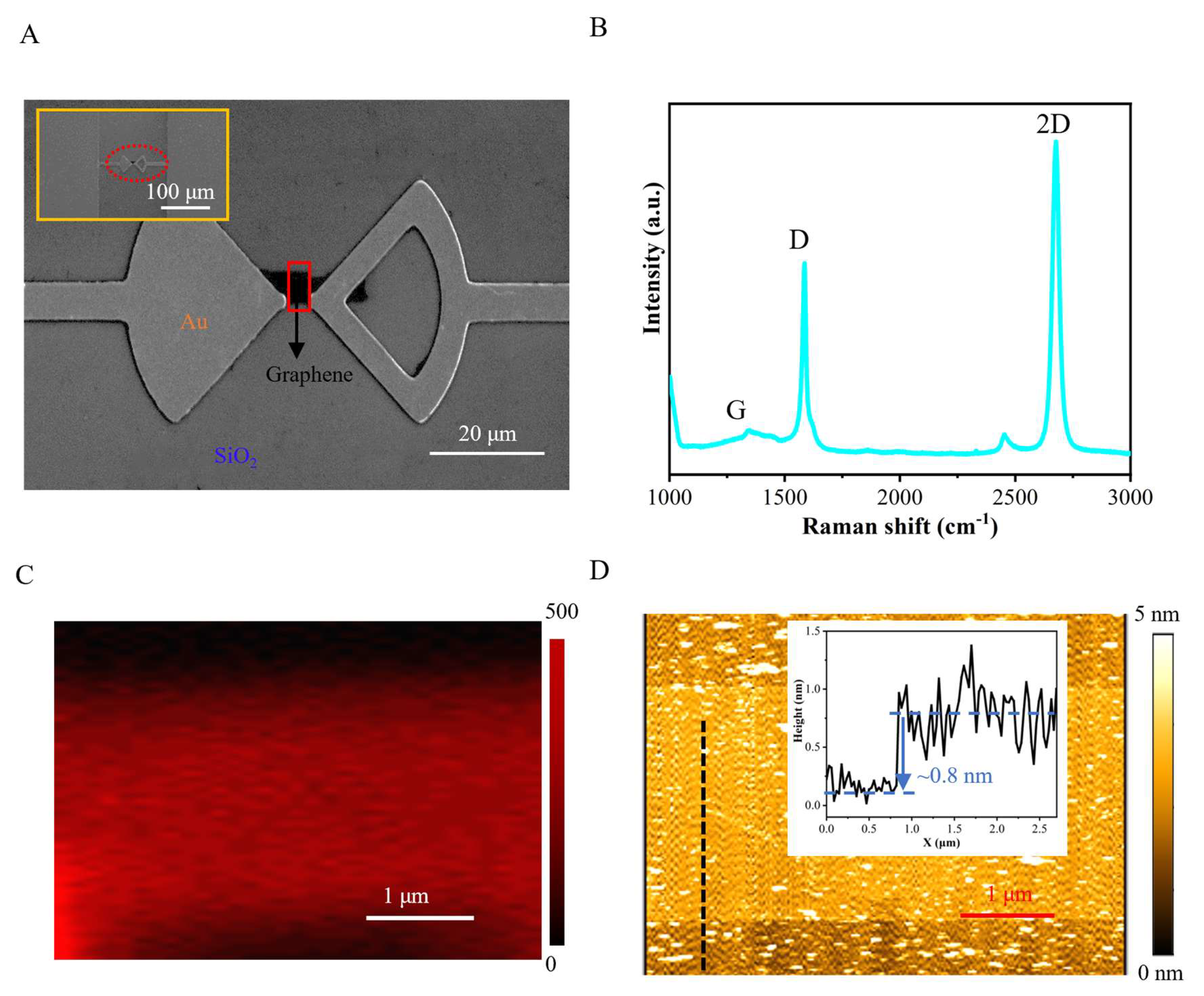
A typical graphene THz detector, as shown in Figure 2A, consists of a patterned graphene flake integrated into the channel region of an asymmetric antenna. The active area of the detector can be determined as ~1500 μm2, which is among the smallest level in various types of THz detectors based on graphene flake coupled with an antenna (Table 1). The graphene layer remains intact throughout the transfer process and detector fabrication, as evidenced by its Raman spectrum (Figure 2B). The Raman modes at 1350 cm−1, 1580 cm−1, and 2700 cm−1 correspond to the G, D, and 2D peaks of monolayer graphene. The intensity ratio between the G peak and the 2D peak at the center of the flake is ≈0.7. In addition, the D peak is relatively small. These features all indicate a high crystallinity and monolayer nature of the graphene [26]. Two–dimensional Raman mapping of the intensity at the 2D peak shows little fluctuation (Figure 2C), further confirming the uniformity and integrity of the graphene flake. The thickness of the graphene monolayer in the channel region is consistent with previous results [27,28], as measured by atomic force microscope (AFM) characterizations (Figure 2D), which show a thickness of 0.8 nm.
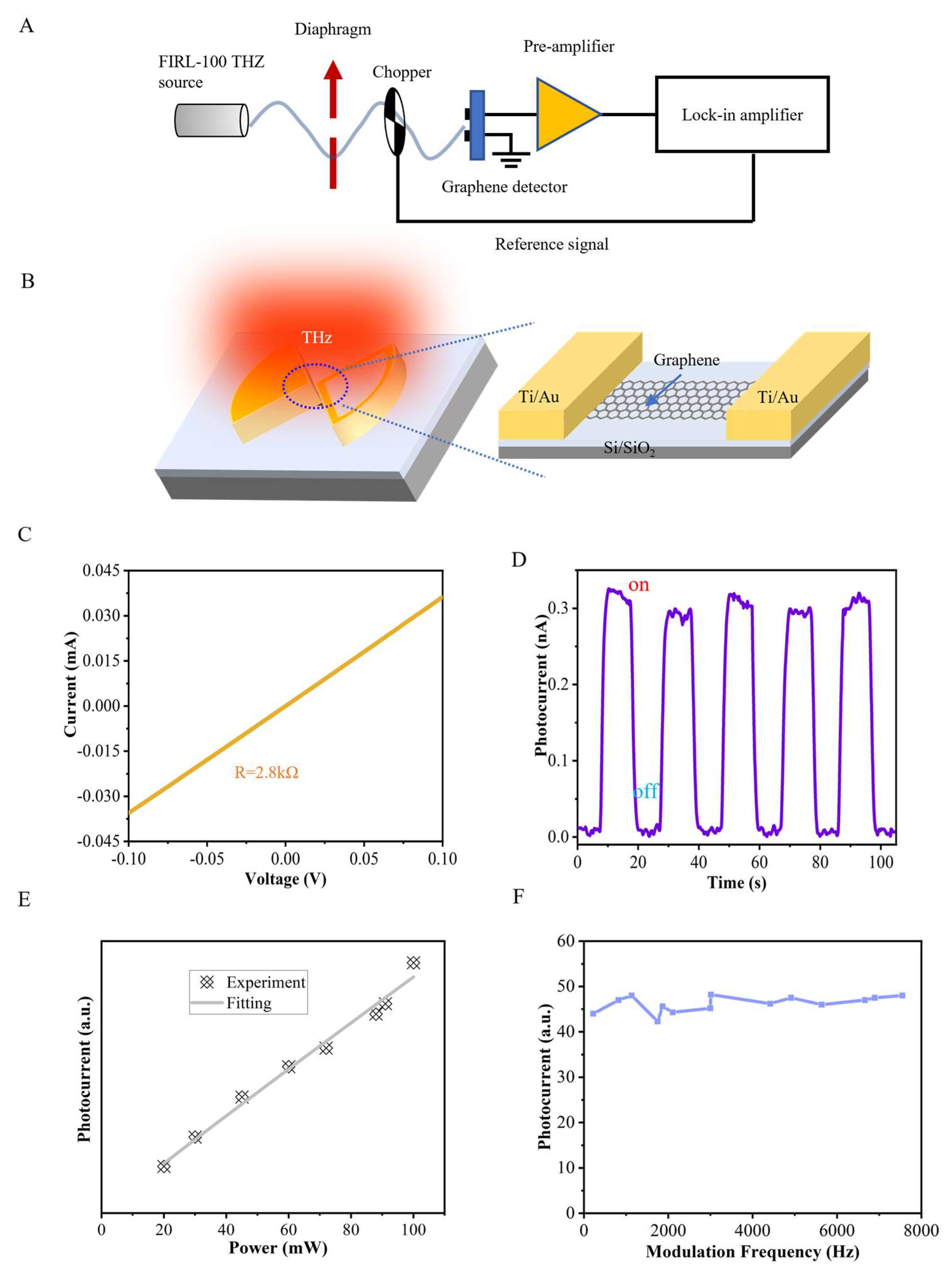
The characterization of the electrical transport and THz detection properties of the graphene detector is illustrated in Figure 3A. In a typical measurement, a chopper–modulated THz radiation illuminates the antenna from the far field. The antenna couples the THz wave and directs the electromagnetic energy into the channel region, where the graphene flake absorbs the energy and generates hot electrons (Figure 3B). The asymmetric coupling efficiency of the antenna results in the uneven generation of hot electrons along the channel region, leading to directional electron flow and the generation of photocurrent.
Figure 3C shows the electrical transport curve of the graphene detector, which exhibits a linear relationship between the current and bias voltage. This suggests that the contact between the graphene monolayer and the antenna is good, likely due to the similar work functions of titanium and CVD–grown graphene. The calculated resistance of the graphene is R = 2800 Ω, indicating good conductivity of the channel and contributing to the evident THz responses of the detector. In Figure 3D, it is shown that the graphene detector exhibits a photocurrent response upon 2.52 THz illumination with a power density of 32 mW/mm2, even at zero bias. The maximum photocurrent recorded was 0.33 nA, while the dark current was 3 pA, resulting in a high signal–to–noise ratio (SNR) of over 100. The photodetection performance of the device is repeatable and stable, as evidenced by the similar responses over five ON/OFF cycles.
The voltage responsivity can be calculated as Rv = RIphSb/(PSa), where R is the resistance of the graphene; Sa is the active area of the detector, which is 0.0015 mm2; and Sb is the radiation beam cross–sectional area, which is determined as 0.8 mm2 using the blade method. Parameter P is the incident power (25 mW) at 2.52 THz. By assuming that the entire power illuminating the antenna is fully coupled to the graphene layer, the Rv of the detector can be calculated as 19.6 V/W. The corresponding current responsivity can be calculated as 0.007 A/W according to RI = Rv /R. With the information of Rv, the noise–equivalent power (NEP), which is a pivotal parameter characterizing the sensitivity of a photodetector, can be calculated as [24],
N E P = 4 k B T R R v
where kB is the Boltzmann constant, R is the resistance of the detector, and T = 300 K. The NEP of the graphene THz detector can be calculated as 590 pW/Hz1/2. In addition, the photocurrent increases against illumination intensity. As shown in Figure 3E, the photocurrent is linearly dependent on the laser intensity in the range of 20 to 100 mW. The response time (RT) of the photodetector can be determined according to the dependence of the photocurrent on the modulation frequency (via adjusting chopper speed). As shown in Figure 3F, the photocurrent of the graphene detector is almost invariant for a modulation up to 7.5 kHz. According to the relationships between responsivity and modulation frequency [32],
R f = R 0 1 + 4 π 2 f 2 τ 2 1 / 2
where τ represents the response time, and R0 is the responsivity at low frequency. The invariant of the responsivity of our detector up to 7.5 kHz modulation speed indicates that the device has an RT of less than 21 μs. Although such value is moderate among the various graphene THz detectors (Table 1), it is believed that the RT can be as small as a picosecond scale according to the theoretical limitation set by the photo–thermoelectric effect [14,19]. However, the chopping frequency of the chopper used in our study cannot be too high, making it impossible to characterize such a high RT. Overall, these results demonstrate the high performance of the graphene detector in detecting THz waves, with high sensitivity, good stability, and fast response time.
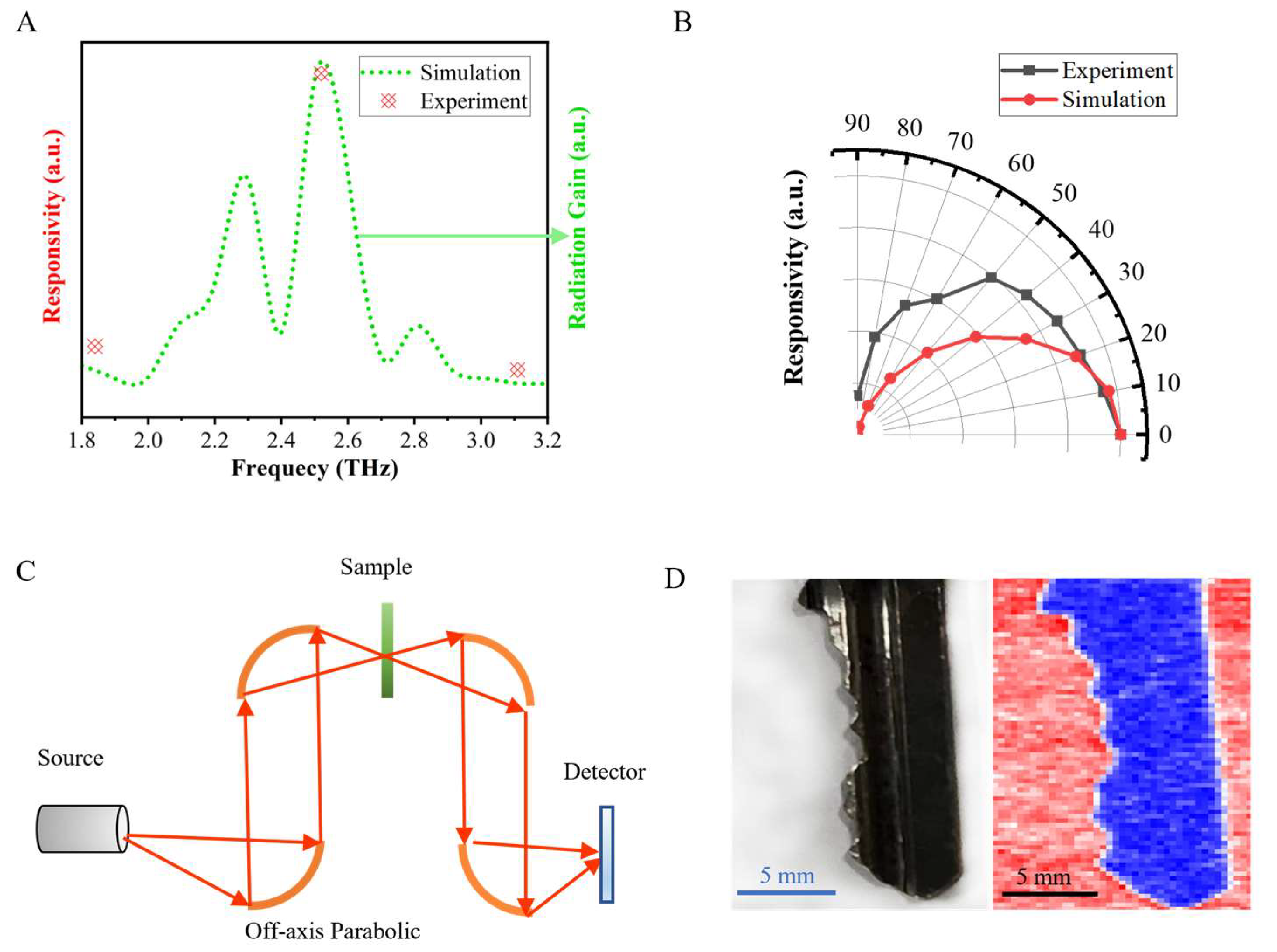
We further conducted the spectral– and polarization–resolved characterization of the graphene detector. To this end, we measured the photocurrent of the device under different THz illumination frequencies, including 1.84 THz, 2.52 THz, and 3.11 THz. The results showed that the responsivity of the detector strongly depends on the incident frequency, with the highest response observed at 2.52 THz (as shown in Figure 4A). This is consistent with the simulated spectral dependence of the radiation gain of the asymmetric bowtie antenna, which is defined as the far–field electric field intensity of the THz field radiating along the normal direction of the substrate (indicated by the dashed green line in Figure 4A). Therefore, the spectral photocurrent response of the graphene detector can be optimized by adjusting the geometry of the antenna to match the specific frequency range of interest. To measure the polarization dependence of the photocurrent, the device was rotated with respect to the polarization direction of the incident THz wave, which was linearly polarized. The detector displayed an anisotropic photocurrent response to polarized irradiation at 2.52 THz, with the maximum response observed along the longitudinal direction of the antenna (x-axis) (as shown in Figure 4B). This polarization behavior can be attributed to the anisotropic electric field localization induced by the antenna. Specifically, by averaging the simulated electric field intensity at the two tips of the bowtie antenna, one can see that the electric field exhibits the same polarization dependence as the photocurrent (as indicated by the red line and dots in Figure 4B). The degree of polarization can be calculated according to the formula P = I M a x I M i n I M a x + I M i n , with IMax and IMin representing the photocurrent corresponding to polarization excitation along the x-axis and y-axis, respectively. The calculated value of P was 0.74, indicating good polarization–resolved THz detection capability.
To demonstrate the practical application of the graphene THz detector, THz imaging was carried out by raster scanning the detector upon 2.52 THz illumination. Specifically, the THz beam was focused by two parabolic mirrors onto a metallic key. The transmitted wave was then expanded and guided by another set of mirrors to the THz detector. The key was mounted onto a stage and scanned at a speed of 2 mm/s (as shown in Figure 4C). A THz photocurrent image of 76 × 50 pixels could then be obtained, which clearly identified and distinguished the shape features of the key. By analyzing the full width at half maximum (FWHM) of a specific pixel in the grayscale image, we can determine that the spatial resolution of the THz imaging can reach ~200 μm. In this system, a graphene–based terahertz detector with a detection element area of 1500 μm2 for high–sensitivity imaging. The small detection element area enabled stable imaging performance. As a potential detection element in a THz focal plane array for staring imaging, this detector offers several advantages, including improved integration and the ability to achieve high–resolution and high–precision imaging.
The results above clearly demonstrate that a room–temperature THz detector has been realized by integrating monolayer graphene with an asymmetric bowtie antenna. For practical applications, especially in THz imaging applications, the THz detector array, i.e., the focal plane array (FPA), is in great demand. FPA is preferred for revealing hidden worlds in astronomy and detecting previously invisible details in biological samples. Our proposed detector is based on graphene grown by the CVD method, where the graphene flake can be of wafer scale size. Such a large and uniform graphene layer makes it possible to design and fabricate FPA using the detector pixel as that proposed in our current study. We will conduct such studies in the coming future.
According to the comparison of performances of THz detectors based on graphene integrated with different antennae in Table 1, our detector may not have the highest responsivity compared to other detectors. This is reasonable because the detector performance is heavily dependent on the physical property and quality of the graphene used. For example, some of the detectors mentioned in Table 1 utilize graphene prepared by mechanical exfoliation [20,21,30], which typically results in high–quality graphene but is challenging to use for large–area array applications. Additionally, some detectors require complex grid structures and external gate voltages in order to achieve higher responsivity [20,21,31]. This will complicate the fabrication processes of the detector, making it difficult to develop detector arrays. Our device, on the other hand, utilizes CVD–grown graphene, which can favor array fabrication. Moreover, through the use of an asymmetric bowtie antenna with a simple detector structure and a small active area, we were able to achieve THz detection and stable, high–sensitivity imaging. This provides promising support for future research and applications of high–performance THz detectors.

4. Conclusions

In summary, we have developed a THz detector by integrating CVD–grown graphene with an asymmetric bowtie antenna. The asymmetry of the antenna coupling efficiency allows for inequivalent THz absorption along the channel region of the graphene, resulting in photocurrent responses in the range of 1.8 THz to 3.2 THz. The maximum responsivity can reach 19.6 V/W at 2.52 THz, with an NEP of 590 pW/Hz1/2 and a response time of less than 21 μs. The SNR can reach up to 100. By taking advantage of the small footprint of the detector, we further demonstrate its potential application in high–spatial–resolution THz imaging. We believe that these results will be essential for the development of high–performance THz detectors using graphene and other types of 2D crystals.

Author Contributions

H.C., S.Z. and S.D. conceived the study. Z.G. fabricated the graphene detector, performed the THz detection and imaging characterizations, and analyzed the data. C.M. designed the asymmetric bowtie antenna. H.O., X.W. and S.L. conducted the Raman spectroscopy, SEM, and AFM characterizations. H.C., S.Z. and S.D. analyzed the data and discussed the results. The manuscript was written through contributions from all authors. All authors have read and agreed to the published version of the manuscript.

Funding

This work was financially supported by the National Key Basic Research Program of China (grant nos. 2019YFA0210200 and 2019YFA0210203), the National Natural Science Foundation of China (grant no. 91963205), and the Guangdong Basic and Applied Basic Research Foundation (grant no. 2023A1515011876). H.C. and S.Z. acknowledge the support from the Cheung Kong Young Scholars Program.

Institutional Review Board Statement

Not applicable.

Informed Consent Statement

Not applicable.

Data Availability Statement

Relevant data supporting the key findings of this study are available within the article. All raw data generated during the current study are available from the corresponding author H.C. upon request.

Conflicts of Interest

The authors declare no conflict of interest.

References

  1. Hafez, H.A.; Chai, X.; Ibrahim, A.; Mondal, S.; Ferachou, D.; Ropagnol, X.; Ozaki, T. Intense Terahertz Radiation and Their Applications. J. Opt. 2016, 18, 093004. [Google Scholar] [CrossRef]
  2. Xu, W.; Xie, L.; Ying, Y. Mechanisms and Applications of Terahertz Metamaterial Sensing: A Review. Nanoscale 2017, 9, 13864–13878. [Google Scholar] [CrossRef] [PubMed]
  3. Yang, X.; Zhao, X.; Yang, K.; Liu, Y.; Liu, Y.; Fu, W.; Luo, Y. Biomedical Applications of Terahertz Spectroscopy and Imaging. Trends Biotechnol. 2016, 34, 810–824. [Google Scholar] [CrossRef] [PubMed]
  4. Zhong, S. Progress in Terahertz Nondestructive Testing: A Review. Front. Mech. Eng. Prc. 2019, 14, 273–281. [Google Scholar] [CrossRef]
  5. Dhillon, S.S.; Vitiello, M.S.; Linfield, E.H.; Davies, A.G.; Hoffmann, M.C.; Booske, J.; Paoloni, C.; Gensch, M.; Weightman, P.; Williams, G.P.; et al. The 2017 Terahertz Science and Technology Roadmap. J. Phys. D-Appl. Phys. 2017, 50, 043001. [Google Scholar] [CrossRef]
  6. Rogalski, A. Progress in Performance Development of Room Temperature Direct Terahertz Detectors. J. Infrared Millim. Terahertz Waves. 2022, 43, 709–727. [Google Scholar] [CrossRef]
  7. Wang, J.; Gou, J.; Li, W. Preparation of room temperature terahertz detector with lithium tantalate crystal and thin film. AIP Adv. 2014, 4, 027106. [Google Scholar] [CrossRef]
  8. Wang, J.; Li, W.; Gou, J.; Wu, Z.; Jiang, Y. Fabrication and parameters calculation of room temperature terahertz detector with micro–bridge structure. J. Infrared Millim. Terahertz Waves 2015, 36, 49–59. [Google Scholar] [CrossRef]
  9. Xiao, P.; Tu, X.; Jiang, C.; Li, Z.; Zhou, S.; Pan, D.; Zhao, Q.; Jia, X.; Zhang, L.; Kang, L.; et al. Planar double–slot antenna integrated into a Nb 5 N 6 microbolometer THz detector. Opt. Lett. 2022, 45, 2894–2897. [Google Scholar] [CrossRef]
  10. Al Hadi, R.; Sherry, H.; Grzyb, J.; Zhao, Y.; Foerster, W.; Keller, H.M.; Cathelin, A.; Kaiser, A.; Pfeiffer, U.R. A 1 k–Pixel Video Camera for 0.7–1.1 Terahertz Imaging Applications in 65–nm CMOS. IEEE J. Solid-State Circuits 2012, 47, 2999–3012. [Google Scholar] [CrossRef]
  11. Ojefors, E.; Pfeiffer, U.R.; Lisauskas, A.; Roskos, H.G. A 0.65 THz Focal–Plane Array in a Quarter–Micron CMOS Process Technology. IEEE J. Solid-State Circuits 2009, 44, 1968–1976. [Google Scholar] [CrossRef]
  12. Zhang, Z.–Z.; Li, H.; Cao, J.–C. Ultrafast Terahertz Detectors. Acta Phys. Sin.-Ch. Ed. 2018, 67, 1–12. [Google Scholar] [CrossRef]
  13. Yang, J.; Qin, H.; Zhang, K. Emerging Terahertz Photodetectors Based on Two–Dimensional Materials. Opt. Commun. 2018, 406, 36–43. [Google Scholar] [CrossRef]
  14. Wang, J.; Xie, Z.; Yeow, J.T.W. Two–Dimensional Materials Applied for Room–Temperature Thermoelectric Photodetectors. Mater. Res. Express. 2020, 7, 112001. [Google Scholar] [CrossRef]
  15. Wang, Y.; Wu, W.; Zhao, Z. Recent Progress and Remaining Challenges of 2D Material–Based Terahertz Detectors. Infrared Phys. Techn. 2019, 102, 103024. [Google Scholar] [CrossRef]
  16. Bae, S.–H.; Kum, H.; Kong, W.; Kim, Y.; Choi, C.; Lee, B.; Lin, P.; Park, Y.; Kim, J. Integration of Bulk Materials with Two–Dimensional Materials for Physical Coupling and Applications. Nat. Mater. 2019, 18, 550–560. [Google Scholar] [CrossRef]
  17. Vicarelli, L.; Vitiello, M.S.; Coquillat, D.; Lombardo, A.; Ferrari, A.C.; Knap, W.; Polini, M.; Pellegrini, V.; Tredicucci, A. Graphene Field–Effect Transistors As Room–Temperature Terahertz Detectors. Nat. Mater. 2012, 11, 865–871. [Google Scholar] [CrossRef]
  18. Sizov, F.; Rogalski, A. THz Detectors. Prog. Quant. Electron. 2010, 34, 278–347. [Google Scholar] [CrossRef]
  19. Freitag, M.; Low, T.; Xia, F.; Avouris, P. Photoconductivity of Biased Graphene. Nat. Photonics 2013, 7, 53–59. [Google Scholar] [CrossRef]
  20. Castilla, S.; Terres, B.; Autore, M.; Viti, L.; Li, J.; Nikitin, A.Y.; Vangelidis, I.; Watanabe, K.; Taniguchi, T.; Lidorikis, E.; et al. Fast and Sensitive Terahertz Detection Using an Antenna–Integrated Graphene PN Junction. Nano Lett. 2019, 19, 2765–2773. [Google Scholar] [CrossRef]
  21. Viti, L.; Purdie, D.G.; Lombardo, A.; Ferrari, A.C.; Vitiello, M.S. HBN–Encapsulated, Graphene–based, Room–temperature Terahertz Receivers, with High Speed and Low Noise. Nano Lett. 2020, 20, 3169–3177. [Google Scholar] [CrossRef]
  22. Liu, C.–H.; Chang, Y.–C.; Norris, T.B.; Zhong, Z. Graphene Photodetectors with Ultra–Broadband and High Responsivity at Room Temperature. Nat. Nanotechnol. 2014, 9, 273–278. [Google Scholar] [CrossRef] [PubMed]
  23. Degl’Innocenti, R.; Xiao, L.; Jessop, D.S.; Kindness, S.J.; Ren, Y.; Lin, H.; Zeitler, J.A.; Alexander–Webber, J.A.; Joyce, H.J.; Braeuninger–Weimer, P.; et al. Fast Room–Temperature Detection of Terahertz Quantum Cascade Lasers with Graphene–Loaded Bow–Tie Plasmonic Antenna Arrays. ACS Photonics 2016, 3, 1747–1753. [Google Scholar] [CrossRef]
  24. Guo, W.; Wang, L.; Chen, X.; Liu, C.; Tang, W.; Guo, C.; Wang, J.; Lu, W. Graphene–Based Broadband Terahertz Detector Integrated with A Square–Spiral Antenna. Opt. Lett. 2018, 43, 1647–1650. [Google Scholar] [CrossRef]
  25. Bean, J.A.; Tiwari, B.; Szakmany, G.; Bernstein, G.H.; Fay, P.; Porod, W. Antenna Length and Polarization Response of Antenna–Coupled MOM Diode Infrared Detectors. Infrared Phys. Techn. 2010, 53, 182–185. [Google Scholar] [CrossRef]
  26. Pan, G.; Li, B.; Heath, M.; Horsell, D.; Wears, M.L.; Al Taan, L.; Alwan, S. Transfer–Free Growth of Graphene on SiO2 Insulator Substrate from Sputtered Carbon and Nickel Films. Carbon 2013, 65, 349–358. [Google Scholar] [CrossRef]
  27. Giannazzo, F.; Sonde, S.; Raineri, V.; Patane, G.; Compagnini, G.; Aliotta, F.; Ponterio, R.; Rimini, E. In Optical, Morphological and Spectroscopic Characterization of Graphene on SiO2. In Proceedings of the 23rd International Conference on Amorphous and Nanocrystalline Semiconductors (ICANS23), Utrecht, The Netherlands, 23–28 August 2010; pp. 1251–1255. [Google Scholar]
  28. Zhou, L.; Fox, L.; Wlodek, M.; Islas, L.; Slastanova, A.; Robles, E.; Bikondoa, O.; Harniman, R.; Fox, N.; Cattelan, M.; et al. Surface Structure of Few Layer Graphene. Carbon 2018, 136, 255–261. [Google Scholar] [CrossRef]
  29. Generalov, A.A.; Andersson, M.A.; Yang, X.; Vorobiev, A.; Stake, J. A 400–GHz Graphene FET Detector. IEEE Trans. Terahertz Sci. Technol. 2017, 7, 614–616. [Google Scholar] [CrossRef]
  30. Tong, J.; Muthee, M.; Chen, S.–Y.; Yngvesson, S.K.; Yan, J. Antenna Enhanced Graphene THz Emitter and Detector. Nano Lett. 2015, 15, 5295–5301. [Google Scholar] [CrossRef]
  31. Qin, H.; Sun, J.; Liang, S.; Li, X.; Yang, X.; He, Z.; Yu, C.; Feng, Z. Room–Temperature, Low–Impedance and High–Sensitivity Terahertz Direct Detector Based on Bilayer Graphene Field–Effect Transistor. Carbon 2017, 116, 760–765. [Google Scholar] [CrossRef]
  32. Harald, S.; Liu, H.C. Quantum Well Infrared Photodetectors: Physics and Applications; Springer: Berlin/Heidelberg, Germany, 2007. [Google Scholar]
Figure 1. Design of an asymmetric bowtie antenna. (A) Schematic showing the asymmetric antenna used in our study. The dark rectangle indicates the region for integration of monolayer graphene. (B) Simulation result of loss parameter (S11) of the asymmetric antenna in the spectral range from 1.8 THz to 3.2 THz. (C,E) Simulation of the in–plane electric field magnitude distributions, |E(x, y)|, of the asymmetric (C) and symmetric (E) antennas at 2.52 THz. The electric fields were monitored at the x–y cross–section of the antenna. The white rectangles indicate the regions for integration of monolayer graphene. (D) Frequency dependence of the electric field magnitudes of the asymmetric (solid lines) and symmetric (dashed lines) antennas. The electric fields were monitored at the positions marked with purple and grey dots shown in (C,E). (F) Simulation result of loss parameter (S11) of the symmetric antenna in the spectral range from 1.8 THz to 3.2 THz.
Photonics 10 00576 g001
Figure 2. Characterizations of the graphene THz detector. (A) Scanning electron microscopy image of the device structure, showing a graphene flake integrated into the channel region of the asymmetric antenna. Inset: dashed circle indicate the whole device structure. (B) Raman scattering spectrum collected from the center of the graphene in the antenna channel. (C) Two–dimensional Raman mapping of the graphene region in the antenna channel. The mapping is performed according to the intensity at the 2D peak of the graphene monolayer. The mapping region is indicated by the red rectangle shown in (A). (D) Atomic force microscope image of the graphene region (red rectangle) is shown in (A). Inset shows the topology profile along the dashed black line.
Photonics 10 00576 g002
Figure 3. THz detection characteristics of the graphene detector. (A) Schematic showing the characterization of the THz detection characteristics of the graphene detector. (B) Illustration of the interaction of THz wave and the detector composed of monolayer graphene integrated with the asymmetric antenna. (C) Dependence of the electrical current and bias voltage of the THz detector. (D) THz photocurrent of the device in response to 5 typical ON/OFF illumination cycles. (E) Dependence of the THz photocurrent on the incident THz wave power. Grey solid line is a linear fit. (F) Dependence of the THz photocurrent on the modulation frequency.
Photonics 10 00576 g003
Figure 4. Spectral and polarization response of the graphene THz detector. (A) Dependence of the responsivity of the graphene detector on the illumination frequency. The simulated spectral dependence of the radiation gain of the asymmetric bowtie antenna is included for reference (green dashed line). (B) Polar plot of the polarization dependence of the photocurrent generation. The simulated electric field intensity upon different polarization excitation is included for comparison. The electric field intensity was averaged at the two tips of the bowtie antenna. The polar angle is measured with respect to the longitudinal direction of the antenna (x-axis). (C) Schematic showing the raster scanning THz imaging of the detector. (D) THz imaging of a metallic key. All of the measurements and simulations are performed at 2.52 THz.
Photonics 10 00576 g004
Table 1. Comparison of performances of THz detectors based on graphene integrated with different antennae.
Antenna TypeActive AreaOperation FrequencyResponse TimeNEPResponsivity
Spiral antenna [24]0.02 mm20.11–0.3 THz9 μs0.35 nW/Hz1/228 V/W
Dipole antenna [20]0.0045 mm21.8–4.2 THz<30 ns80 pW/Hz1/2105 V/W
Bowtie antenna [21]0.0025 mm23.0 THz≤3.3 ns160 pW/Hz1/249 V/W
Bowtie antenna [29]0.05 mm20.4 THz130 pW/Hz1/274 V/W
Double patch antenna [30]0.0014 mm21.9 THz1.7 nW/Hz1/24.9 V/W
Dipole antenna [31]0.3 THz51 pW/Hz1/230 V/W
Bowtie antenna [23]0.001 mm22.0 THz150 nW/Hz1/234 μA/W
Asymmetric bowtie antenna (This work)0.0015 mm21.8–3.2 THz<21 μs0.59 nW/Hz1/219.6 V/W
(0.007 A/W)
Disclaimer/Publisher’s Note: The statements, opinions and data contained in all publications are solely those of the individual author(s) and contributor(s) and not of MDPI and/or the editor(s). MDPI and/or the editor(s) disclaim responsibility for any injury to people or property resulting from any ideas, methods, instructions or products referred to in the content.

