Article

The Effect of GaSb Substrate Oxidation Layer on InAs/GaSb Type II Superlattice

1
School of Instrument Science and Opto-Electronics Engineering, Beijing Information Science & Technology University, Beijing 100192, China
2
Key Laboratory of the Ministry of Education for Optoelectronic Measurement Technology and Instrument, Beijing 100016, China
3
School of Optoelectronic Engineering, Changchun University of Science and Technology, Changchun 130022, China
4
School of Instrument Science and Opto-Electronics Engineering, Hefei University of Technology, Hefei 230009, China
*
Authors to whom correspondence should be addressed.
Photonics 2023, 10(3), 345; https://doi.org/10.3390/photonics10030345
Submission received: 8 February 2023 / Revised: 3 March 2023 / Accepted: 7 March 2023 / Published: 22 March 2023
(This article belongs to the Special Issue III-V Semiconductors Optoelectronic Materials and Devices)

Abstract

:
Type-II superlattices (T2SLs) are emerging as next-generation materials for infrared detectors. The epitaxial quality of T2SLs is of great importance to the performance of infrared detectors such as dark current and detectivity. Herein, we explore the effect of the native GaSb oxide layer on the surface morphology and crystal quality of InAs/GaSb T2SLs grown with molecular beam epitaxy. The experimental results demonstrate that the thickness of the oxidation layer on GaSb substrates gradually increases over time and is saturated at around 73 Å in the natural oxidation condition. Moreover, the oxidation process is sensitive to humidity. As the thickness of the GaSb oxide layer increases from 18.79 Å to 61.54 Å, the full width at half maximum of the first satellite peak increases from 38.44 to 61.34 arcsec in X-ray diffraction measurements, and the root mean square roughness increases from 0.116 nm to 0.171 nm in atomic force microscopy measurements. Our results suggest that the thickness of the GaSb oxide layer should be less than 55 Å to obtain smooth buffer layers and qualified superlattices. The work provides an optimized direction for achieving high-quality superlattices for infrared optoelectronic devices.

1. Introduction

Infrared photodetectors have become a core technology in gas detection [1], weather warnings [2], medical diagnostics [3], and surveillance [4]. Currently, commercial infrared detector technology is dominated by mercury cadmium telluride (MCT). However, MCT-based infrared detectors are impeded by several bottlenecks. For example, tuning the band gap of HgCdTe needs extremely high precision in the composition of the semiconductor alloy [5], requiring strict control of the growth temperature during the growth process. As a result, the manufacturing yield for MCT large-area focal plane arrays (FPAs) is severely limited. InAs/GaSb type II superlattices (T2SLs), a new III-V material system, are emerging as one of the most promising candidates for next-generation infrared detectors. Most notably, InAs/GaSb T2SLs have an easily tunable bandgap, high manufacturing yield, good stability, and theoretically comparable performance to MCT, so they are regarded as promising candidates for mid- and long-infrared detectors. However, after nearly two decades of development, the performance of InAs/GaSb T2SLs still lags behind that of MCT [6]. Significant efforts have been made to improve the performance of T2SL infrared detectors, including changing the barrier structure [7,8], improving the superlattice quality [9,10], and optimizing the passivation process [11,12]. The superlattice’s quality plays a critical role in leakage currents, minority lifetime, and uniformity. In general, V-III beam flux ratio, growth temperature, and interface engineering layers are usually optimized to reduce the net strain of the superlattice, improve the flatness of the surface morphology, and reduce the crystal defect density [13,14]. However, it is still challenging to obtain a smooth epitaxy surface for T2SLs [15].
GaSb, with a similar lattice constant, is widely used as the substrate for Sb-based T2SLs. Before superlattice growth, a GaSb buffer layer is grown on the substrate to smooth the substrate surface. Four key parameters need to be carefully optimized to eliminate defect formation during buffer layer growth, i.e., the deoxidization temperature, a protected Sb flux during deoxidization, the substrate temperature, and the Ga/Sb flux ratio [16,17]. A GaSb deoxidization temperature, usually between 500 and 550 °C, is adopted to remove the GaSb oxide layer [18,19]. Although a thin oxide layer can be removed during the deoxidation process, an incompletely removed oxide layer leads to an irregular surface, which is one of the main reasons for the surface roughness of the subsequent T2SLs. This effect becomes more severe when the oxide layer becomes thick. Although early studies on GaSb described the oxide species of GaSb [20], they did not shed light on how the GaSb oxide layer affects the superlattice quality.
Herein, we investigate the effect of GaSb substrate oxide layers on the quality of superlattices. During the oxidation process, the thickness of surface oxide species was measured with an ellipsometer, and the binding energy of oxygen atoms was determined with X-ray photoelectron spectroscopy (XPS). The high-quality superlattices grown using well-optimized parameters were confirmed with scanning transmission electron microscopy (STEM). Further, a combination of atomic force microscopy (AFM) and high-resolution X-ray diffraction (HRXRD) characterizations was adopted to study the influence of oxide thickness on the superlattice quality.

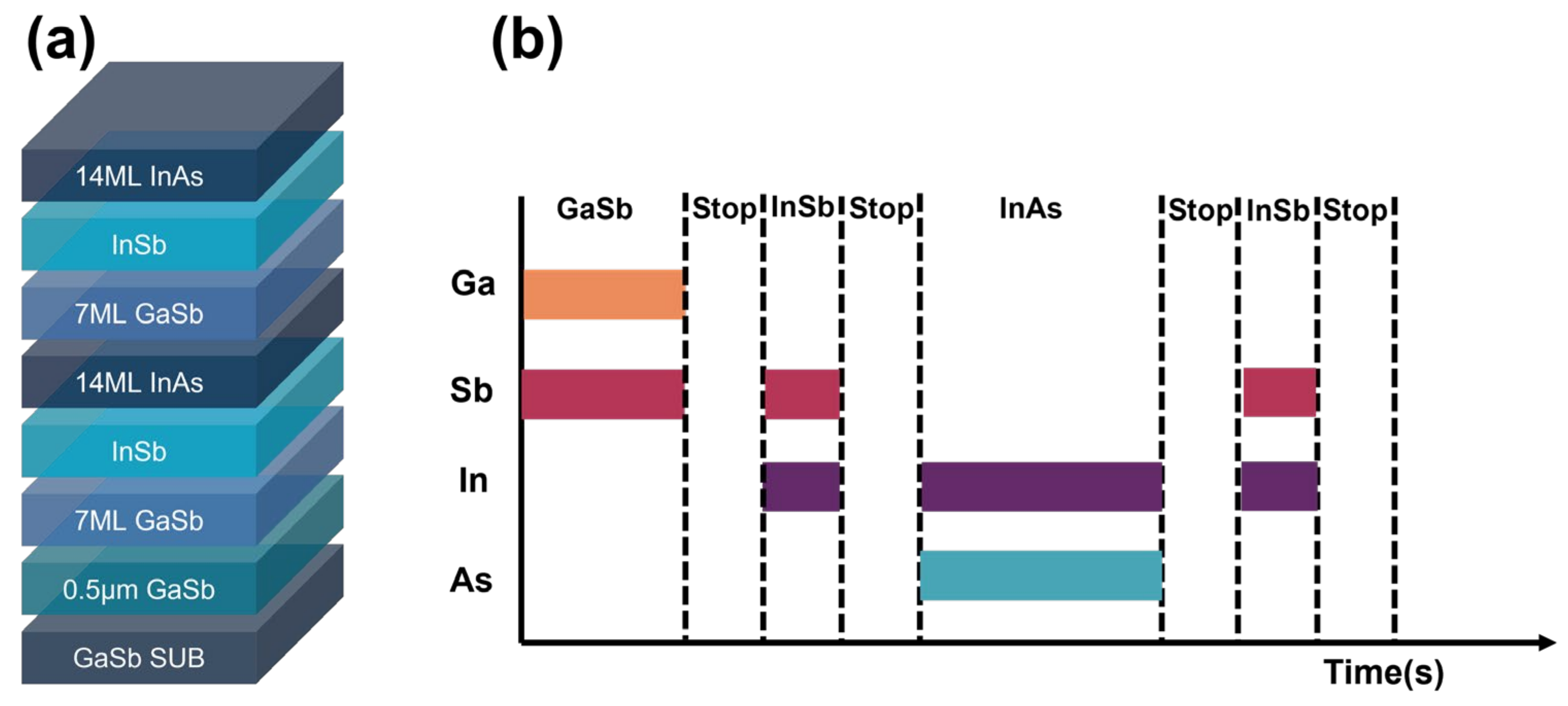
2. Materials and Methods

The 14ML InAs/7ML GaSb superlattices were grown with molecular beam epitaxy (MBE KOMPONENTEN|DR. EBERL Octoplus 400, Weil der Stadt, Germany) on a two-inch double-sided polished GaSb substrate with Te doping. The GaSb substrates were loaded through a load-lock chamber with a base pressure of 10−8 mbar. Then, the samples were transferred into a buffer chamber and heated to 300 °C to remove water and contaminants. When the buffer chamber vacuum reached 9 × 10⁻⁹ mbar, the substrate samples were loaded into the growth chamber. In the growth chamber, the GaSb substrates were deoxidized at 520 °C for 10 min to remove the natural oxide layer on the GaSb surface. At this stage, the GaSb substrate surface was rough, and buffer layers were epitaxially grown on samples to flatten the surface, using a V/III ratio of 5 and 7 for GaSb and InAs, respectively. The deposition rates of GaSb and InAs were 0.112 nm/s and 0.095 nm/s, respectively. In the superlattice deposition period, 14 atomic layers of InAs and 7 atomic layers of GaSb were grown, and the strain between the layers was controlled by inserting a binary alloy, InSb, between the interfaces. The relevant growth details are shown in Figure S1.
The thickness of the oxide layer on the GaSb substrate was studied by using an elliptic spectrometer at different angles (60° and 70°) in the wavelength range of 193 nm to 1690 nm. In order to determine the thickness of the GaSb oxide layer, a structural model consisting of the GaSb substrate and GaSb oxide layer was established.
X-ray photoelectron spectroscopy analysis was obtained in an ultrahigh vacuum (UHV) system (base pressure in 10−10 mbar) with a commercial Omicron ex situ system, and a C1s peak at 284.8 eV was used. The peak fitting of XPS spectra was performed with CasaXPS processing software.
The surface morphology of the films was investigated with atomic force microscopy (OXFORD Instruments, Cypher ES, Abingdon, UK) in noncontact mode and reflection high-energy electron diffraction (RHEED). Selected samples were also characterized using scanning transmission electron microscopy (JEOL JEM-ARM200F, Tokyo, Japan) to investigate dislocations in the superlattice layers, with an acceleration voltage of 220 kV.
Superlattices grown on substrates with different oxide thicknesses were characterized using X-ray diffraction (Malvern Panalytical, X’Pert3 MRD, Malvern, UK); the diffractometer settings were Cu Ka radiation, I = 30 mA, and U = 40 kV.

3. Results and Discussions

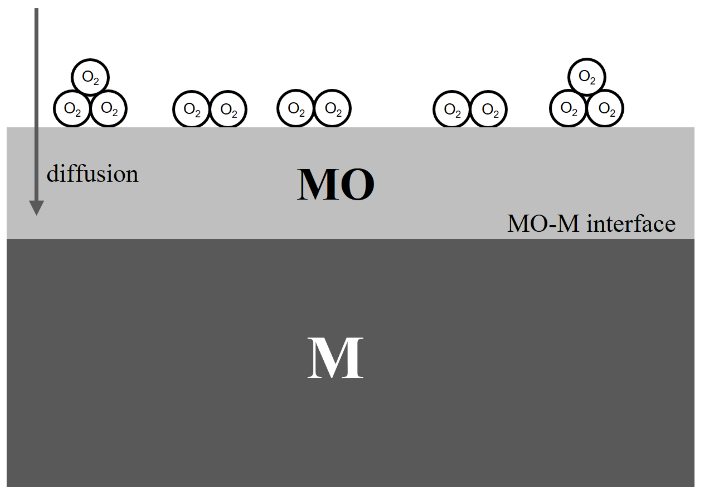
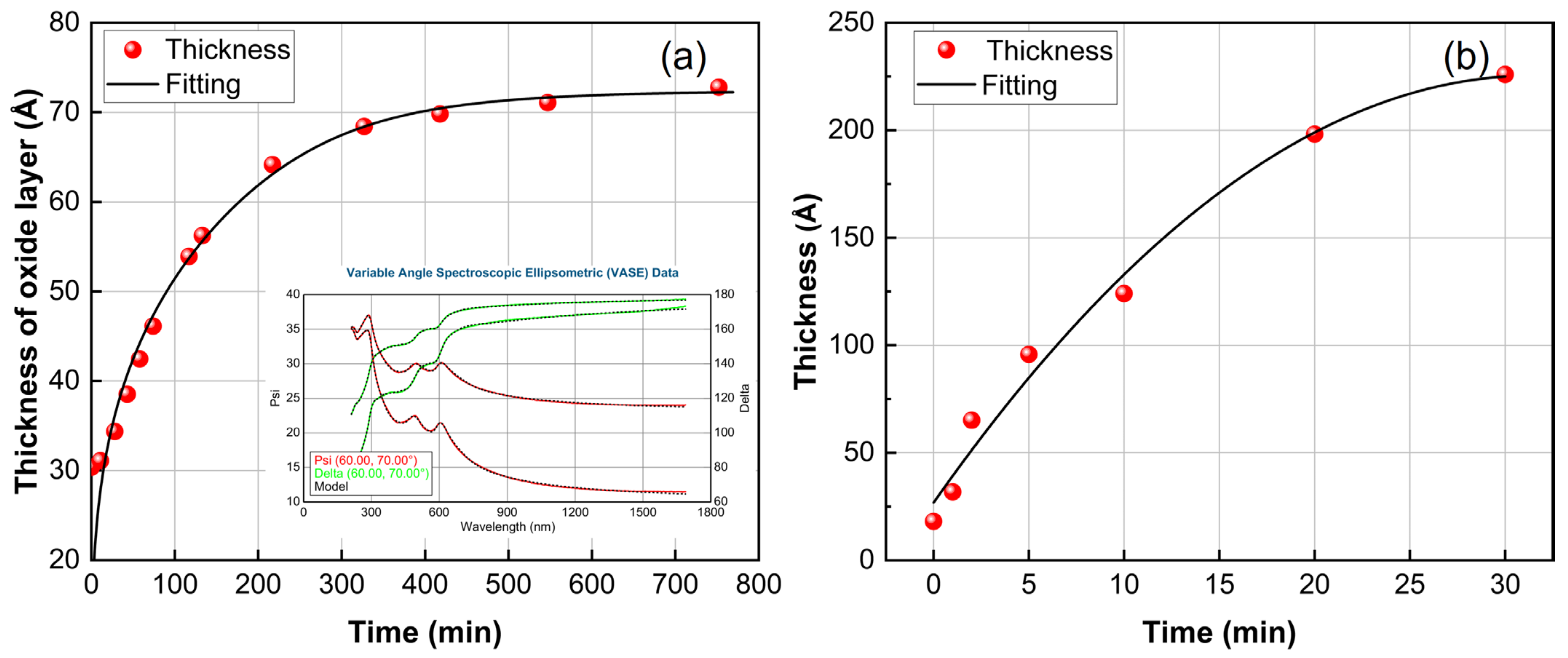
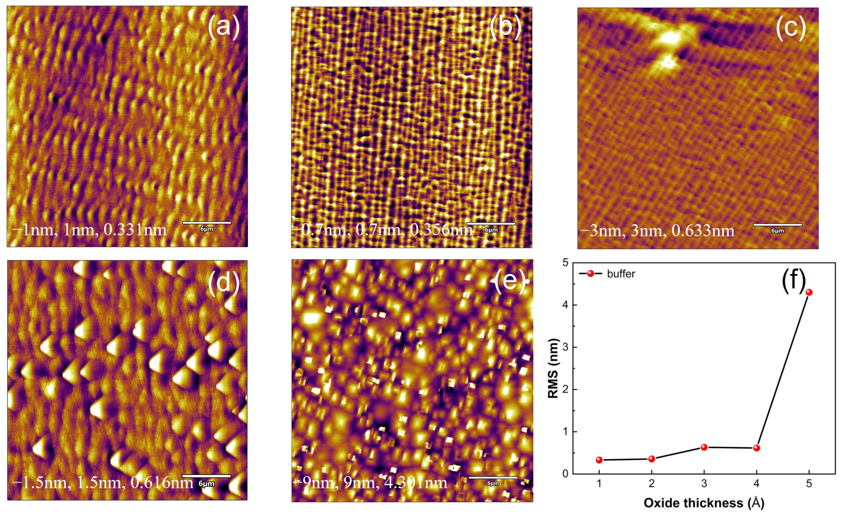
3.1. Analysis of Oxidation Behavior
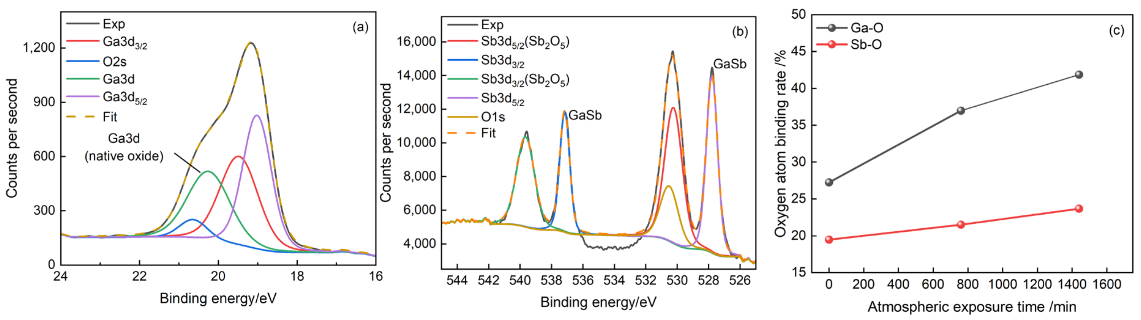
To investigate the trend in the surface oxidation behavior of the GaSb substrates, a fresh GaSb substrate was placed on an ellipsometer stage. The wavelength range 193–1690 nm was chosen to characterize the thickness of the surface oxidation layer. The oxidation process can be divided into two stages. Firstly, oxygen molecules are adsorbed on the substrate surface and diffuse to the interior of the substrate; secondly, oxygen molecules react with the GaSb material. In general, the oxygen molecules’ diffusion process in the first stage follows Fick’s law [21]. Fick’s first law is defined as the number of molecules passing through a unit surface cross-section per unit time, and the planar one-dimensional diffusion flux J is equal to:
J = Δ x 2 2 τ C x + Δ x C x Δ x = D C x x
where τ is the unit time, D is the diffusion coefficient, and C is the concentration in moles or grams per unit volume. Although Fick’s first law defines the rate of diffusion of molecules, it does not give the concentration of a substance as a function of time and cannot describe the nonstationary process of surface oxidation. Instead, Fick’s second law [22,23], derived from Fick’s first law, solves this problem, as shown by the following equation:
x , t t = D 2 x , t x 2
Equation (2) describes the change in molecular concentration with time at a certain point x. The diffusion rate is positively correlated with the diffusion coefficient and the second order derivative of the concentration gradient. When the oxidation rate is greater than the diffusion rate, the oxidation reaction on the substrate surface is determined by diffusion [24]. We set VOxide as the generated GaSb oxide volume and VGasb as the consumed GaSb volume. If the ratio between the volume of GaSb oxide produced and the volume of GaSb consumed is less than 1, that is, VOxide/VGaSb < 1, the oxide is in a porous structure and cannot prevent oxygen molecules from diffusing in the interior. The diffusion reaction on the substrate surface simultaneously occurs with the oxidation reaction, and the dominance gradually changes over time. When VOxide/VGaSb > 1, the oxide layer is dense and can prevent the oxygen molecules from diffusing to the interior and subsequently decreases the oxidation rate. At this stage, the oxygen molecules undergo an oxidation reaction during the diffusion process; therefore, it cannot be simply considered as Fick’s law of diffusion, but should be studied with the aid of gas–solid reactions (including oxidation, catalysis, etc.) [25] The general formula for the oxidation reaction is:
M ( s ) + 1 2 O 2 ( g ) MO ( s )
Figure 1 shows a schematic diagram of the gas–solid reaction, where MO is the oxide produced by the reaction of oxygen with the material M.
To investigate the oxidation process of the GaSb substrate, we utilized ellipsometry to analyze the oxidation behavior of GaSb in natural oxidation and deionized water conditions. In an atmospheric and deionized environment, we used slices of the same fresh substrate. Figure 2a shows that the thickness of the oxide layer in natural oxidation conditions significantly increased in the first 300 min, and the oxidation rate gradually slowed down within the range of 300 to 800 min. Finally, the thickness of the oxide layer was saturated at around 73 Å. While in deionized water, the thickness of the oxide layer exceeded 200 Å in only 30 min, as shown in Figure 2b. Because both conditions were under constant temperature, only the humidity was different, so it can be concluded that humidity had a great influence on the oxidation process.

3.2. Oxide Layer

GaSb materials have a high surface activity, and exposure to air results in the formation of a natural oxide layer consisting of Ga2O3 and Sb2O3. This oxidation begins with breaking the surface atomic bonds and subsequent reconfiguring to form the native oxide layer surface. Oxygen molecules diffuse internally through the surface of the GaSb substrate, a process that reacts with both Ga and Sb to form a nonequilibrium Ga2O3 + Sb2O3 surface oxide layer as follows [26,27]:
2 G a S b + 3 O 2 G a 2 O 3 + S b 2 O 3
As the exposure time increases, the Sb2O3 continuously reacts with GaSb, producing Ga2O3 and free Sb. At this point, the substrate surface oxidation process reaches thermodynamic equilibrium:
S b 2 O 3 + 2 G a S b G a 2 O 3 + 4 S b
The reaction occurring in Equation (5) occurs spontaneously even at room temperature so that a natural oxidation layer consisting of Ga2O3 and free Sb is formed on the surface of GaSb exposed to air. The oxidation of GaSb can then be summarized by the following stoichiometric reactions.
4 G a S b + 3 O 2 2 G a 2 O 3 + 4 S b
To verify the trend in oxide layer growth measured with ellipsometry, the oxidation behavior of the GaSb surfaces in their natural condition was studied with XPS. XPS study of oxidized GaSb can not only show the presence of the elements Ga, Sb, and GaSb, but also the oxidation products Ga2O3, Sb2O3, and Sb2O5 [28]. Therefore, when using XPS to characterize GaSb surface oxides [29,30], we have to analyze the binding rate of oxygen atoms and the GaSb. We measured the XPS curves of the GaSb samples with different atmospheric exposure times, calculated the percentage of the constituent atoms bonded to oxygen, and analyzed the distribution pattern of O on the substrate surface. Figure 3a,b show the splitting of the peaks for the Ga and Sb elements of a fresh sample, respectively. The Ga3d3/2, Ga3d5/2, Sb3d3/2, and Sb3d5/2 come from GaSb. The Ga3d, Sb3d3/2(Sb2O5), and Sb3d5/2(Sb2O5) are attributed oxidation products. We comparably investigated the binding rate of Ga-O and Sb-O changes with exposure time (Figure S2). As can be seen in Figure 3c, with the increase in exposure time, the proportion of oxygen on the surface of the GaSb substrate was gradually enhanced. The experimental value of Ga3d for the surface oxide layer shifted from 19.18 eV to 19.52 eV for fresh samples compared to the GaSb samples exposed to the atmosphere for 760 min, and the experimental value of Sb3d5/2 shifted from 530.26 eV to 531.24 eV. The overall trend is consistent with the curve results of the oxidation process. From the metal as well as Sb3d, a fraction of GaSb is bound to oxygen. As shown in Figure 3,b, remainder of intensity under at Sb3d5/2(Sb2O5) energy can be attributed to oxygen. (O1s).

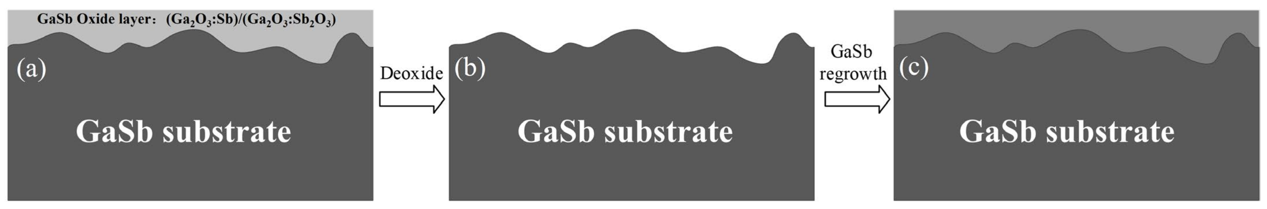
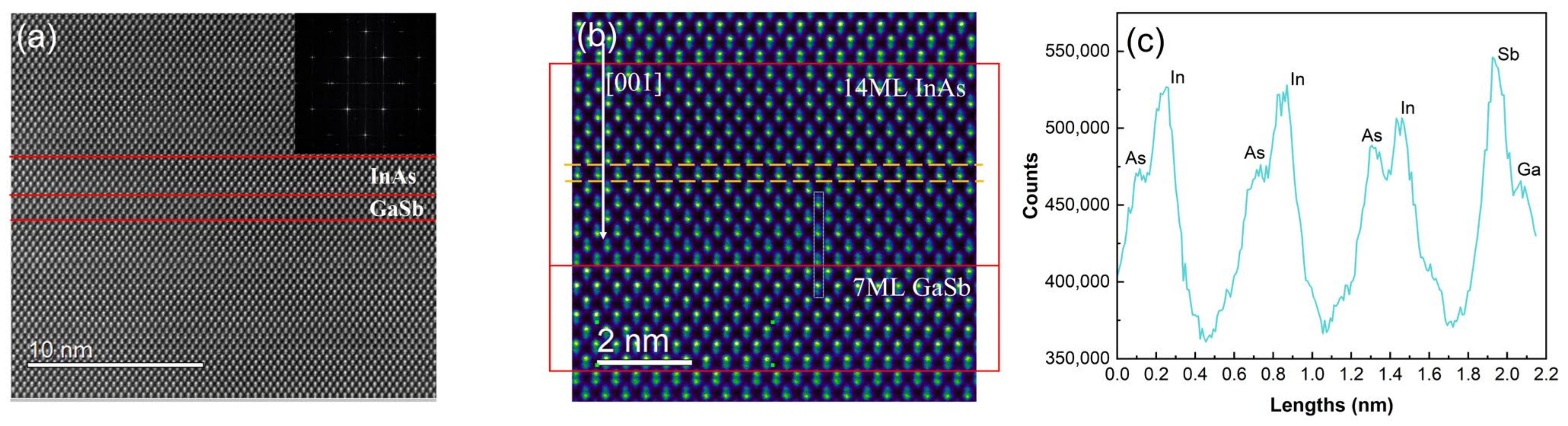
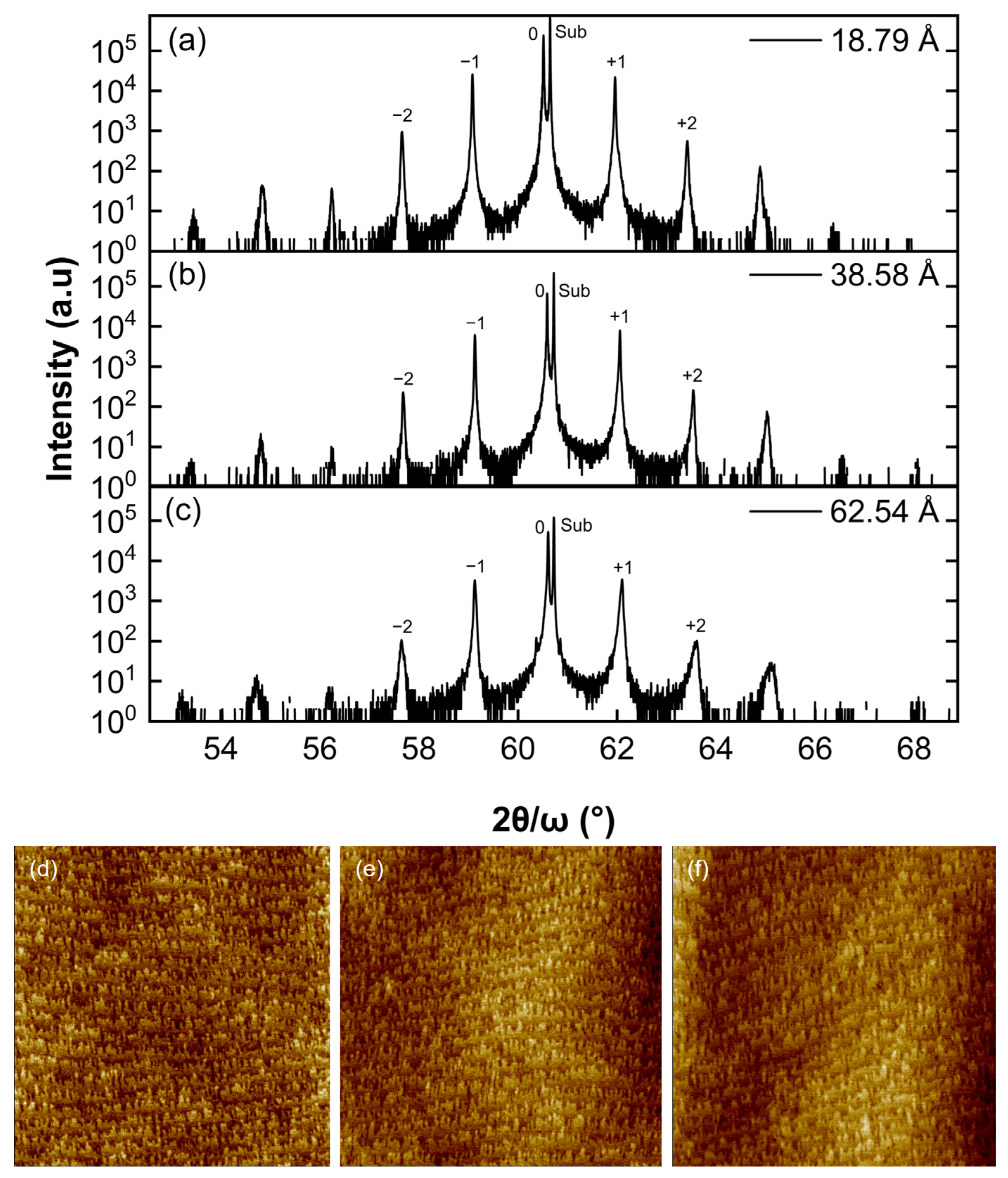
3.3. Epitaxial Layer

The growth of thin films on GaSb substrates with molecular beam epitaxy involves a series of surface processes. Driven by the surface dynamics process, the Ga and Sb atoms adsorbed to the substrate surface migrate, diffuse, desorb, and finally combine to form a most stable state. Before atomic deposition, the substrate needs to be pretreated with three steps. The first step is degassing, in which gas molecules adsorbed on the GaSb substrate are removed by heating the substrate to a moderate temperature (~140 °C). The second step is deoxidizing; a high temperature (~520 °C for GaSb) is required to remove the substrate surface oxides as much as possible. However, the surface of the substrate is very rough at this state due to the erosion of the GaSb surface by oxygen atoms. We used RHEED to monitor the substrate surface and analyze the phase transitions during surface reconstruction (as shown in Figure S3). The last stage is the epitaxy of a GaSb buffer layer on the deoxidized substrate to smooth the surface of the substrate. This stage mainly prepares the substrates for the subsequent epitaxy of superlattices and makes the growth surface smoother, as shown in Figure 4.
To explore the effect of GaSb oxide layers, we investigated five substrate samples for buffer epitaxial layer growth, corresponding to GaSb oxide layer thicknesses of 18.21 Å, 38.34 Å, 55.76 Å, 115.63 Å, and 224.71 Å, respectively. The pretreated samples a, b, c, d, and e were transferred into the MBE chamber for degassing and deoxidation. All samples were deoxidized at 520 °C for 10 min, and a 500 nm GaSb buffer layer was epitaxially grown on each sample. Five samples with different oxide layer thicknesses were successively epitaxially grown one by one in the same time period. As shown in Figure 5, due to the difference in the native oxide layer thickness, the surface of the samples remarkably changed. The fluctuation degree of samples a and b was less than ±1 nm and the uniformity was good in the whole range of 30 × 30 μm, as displayed in Figure 5a,b. However, it can be seen in Figure 5c that there was an obvious protrusion on the surface of sample c, and the RMS sharply increased to 0.633 nm. When the thickness of the GaSb oxide layer approached 115.63 Å, a number of pyramids were observed, as shown in Figure 5d. We found that when the native oxide layer was even larger, as shown in Figure 5e, the buffer layer surface showed more bumps, and the maximum fluctuation height and RMS reached 9 nm and 4.301 nm, respectively. These values are about one thousand times larger than those of samples a and b. Figure 5f concludes that the RMS changed with the thickness of the GaSb oxide layer. When the GaSb oxide layer was very thin, the RMS slightly increased with the surface oxide layer thickness, and there were no obvious pyramids that could be observed. When the thickness of the surface oxide layer reached 55 Å, the overall surface quality significantly declined, and pyramids began to emerge. Therefore, from AFM characterization, the critical thickness of the surface oxide layer for obtaining a smooth surface morphology is below 55 Å. The deep oxidation degree not only makes the deoxidized surface rough, but also leads to serious defects, as it is difficult to completely remove the oxide layer (as shown in Figure S4).
Figure 5 illustrates that the thickness of native oxide on the substrates had a great influence on the growth of the buffer layer. Further, we investigated the effect of the native oxide on the subsequent heterogeneous epitaxy of T2SLs. A long-infrared T2SL (14ML InAs/7ML GaSb) was chosen. The superlattice structure and the epitaxy procedure are shown in Figure 6. A 100-period superlattice was epitaxially grown on GaSb substrates with native oxide layers of 18.79 Å, 38.58 Å, and 62.54 Å, respectively, with a waiting time of 0.5 s before and after each switch of the shutter, as shown in Figure 6b, which provided enough time for the atoms to migrate a long enough distance and reduced elemental intermixing in the growth.
To verify the superlattice quality, we chose fresh GaSb substrates to grow the InAs/GaSb superlattice. The periodic structure of the superlattice was characterized with STEM. As shown in Figure 7a, the InAs and GaSb lattices were well matched, the interface was homogeneous, and there was no obvious dislocation. The diffraction pattern of the sample is given in the upper right corner. The atomic layers contained in one InAs/GaSb superlattice cycle are shown in Figure 7b, showing 21 atomic layers in agreement with the design values; both Figure 7a,b imply that the superlattice had a good crystal quality. The yellow dashed line in Figure 7b shows the intentionally inserted InSb interface during the superlattice growth. The InSb layer was mainly used to balance the lattice mismatch between InAs and GaSb in the superlattice. In a superlattice period, a total of 1.3ML of InSb layers was divided into two interfaces. Figure 7c shows a qualitative analysis of the intensity of the atomic columns in the high-angle annular dark-field (HAADF) image using the Digital Micrograph software. The HAADF image shows the Z-contrast, in other words, the contrast that varies according to the atomic number of the element to judge the element species [31]. The atomic column intensities are significantly lower for the triplet elements in the chemical periodic table than for the fifth group elements, where the atomic numbers of Ga, In, As, and Sb are 39, 49, 33, 51, respectively, thus marking the different distribution of elements on the peaks. The STEM results confirmed that the superlattice material had an excellent interlayer structure and no other microstructural defects were present, proving an excellent experimental platform for studying the oxide layer. Since the superlattice quality can also be analyzed with X-ray diffraction, we chose to use X-ray diffraction to characterize the superlattices grown on substrates with oxide layers of different thicknesses.
Then, we used HRXRD to characterize the superlattices grown on substrates with oxide layers of different thicknesses [32]. All measurements were taken at room temperature (300 K). The rocking curve on the (004) of the InAs/GaSb superlattice is shown in Figure 8. The net strain of all superlattice samples was less than 0.2%. The full width at half maximum (FWHM) of the zero-order peaks of samples (a), (b) and (c) are 26.7 arcsec, 27.8 arcsec and 34.7 arcsec, respectively. This is consistent with the trend in the native oxidation layer thickening. In addition, the first-order satellite peak in Figure 8c showed a significant increase in FWHM and a decrease in satellite peak intensity. This indicates that the superlattice quality of samples with 62.54 Å oxide layer thickness was worse, which is attributed to the oxidation layer being too thick to be completely removed. According to the trend shown in Figure 5, the poor surface morphology after deoxygenation is reflected on the epitaxy layer, and the quality of the epitaxy superlattice is eligible when the oxide layer thickness is less than 55 Å. Figure 8d–f corresponds to the AFM images of the superlattice (a), (b) and (c) in the 1 × 1 μm range, respectively. The RMS of samples a, b, and c are 0.116 nm, 0.144 nm, and 0.171 nm respectively, indicating that the surface morphology becomes worse with the increase in the native oxide layer thickness [33].

4. Conclusions

In summary, we investigated the effect of the native GaSb oxide layer on the surface morphology and crystal quality of InAs/GaSb T2SLs grown with molecular beam epitaxy. The experimental results demonstrate that the rate of oxidation of GaSb substrates varies in different conditions and considerably depends on the humidity. Atomic force microscopy and high-resolution X-ray diffraction results show that the thickness of the native oxide layer of the substrate affects the surface morphology and crystal quality of the subsequent epitaxial buffer and superlattice layers. Smooth surface topography and high-quality superlattices were obtained below a critical oxide layer thickness of 55 Å. This work successfully demonstrated that the native oxide layer thickness of the substrate is a key factor affecting the quality of the superlattice, and high-quality superlattices can be obtained by using GaSb substrates with thin native oxide layers, which reveals a promising method for improving the performance of infrared detectors.

Supplementary Materials

The following supporting information can be downloaded at: https://www.mdpi.com/article/10.3390/photonics10030345/s1, Figure S1: The growth process of superlattices; Figure S2: The binding rate of Ga and Sb to oxygen under different atmospheric exposure times; Figure S3: Reflection high energy electron diffraction of reconstruction processes; Figure S4: Spiral dislocations on the surface of GaSb buffers grown on GaSb substrates with 224.71 Å oxide thickness were observed by atomic force microscopy.

Author Contributions

Conceptualization, J.L. and Y.L.; methodology, J.L. and X.Z.; software, R.G. and L.L.; validation, J.L. and M.G.; formal analysis, J.L.; investigation, R.G. and Z.C.; resources, D.Z. and Y.F.; data curation, Q.F.; writing—original draft preparation, J.L. and B.L.; writing—review and editing, J.L. and Y.L.; supervision, Y.L. and L.Z.; project administration, Y.L. and L.Z.; funding acquisition, L.Z. All authors have read and agreed to the published version of the manuscript.

Funding

This research was funded by the Young Elite Scientist Sponsorship Program by the China Association for Science and Technology (Grant No. YESS20200146), The Beijing Scholars Program (74A2111113), the Research Project of Beijing Education Committee (KM202111232019), and the National Natural Science Foundation of China (Grant No. 62105039, 52275517).

Institutional Review Board Statement

Not applicable.

Informed Consent Statement

Not applicable.

Data Availability Statement

Some or all data that support the findings of this study are available from the corresponding author upon reasonable request.

Conflicts of Interest

The authors declare no conflict of interest.

References

  1. Clément, Q.; Melkonian, J.-M.; Dherbecourt, J.-B.; Raybaut, M.; Grisard, A.; Lallier, E.; Gérard, B.; Faure, B.; Souhaité, G.; Godard, A. Longwave infrared, single-frequency, tunable, pulsed optical parametric oscillator based on orientation-patterned GaAs for gas sensing. Opt. Lett. 2015, 40, 2676–2679. [Google Scholar] [CrossRef] [PubMed]
  2. Yin, R.; Han, W.; Gao, Z.; Di, D. The evaluation of FY4A’s Geostationary Interferometric Infrared Sounder (GIIRS) long-wave temperature sounding channels using the GRAPES global 4D-Var. Q. J. Roy. Meteor. Soc. 2020, 146, 1459–1476. [Google Scholar] [CrossRef]
  3. Zouboulis, C.C.; da Costa, A.N.; Jemec, G.B.E.; Trebing, D. Long-Wave Medical Infrared Thermography: A Clinical Biomarker of Inflammation in Hidradenitis Suppurativa/Acne Inversa. Dermatology 2019, 235, 144–149. [Google Scholar] [CrossRef] [PubMed]
  4. Ju, Y.J.; Jo, J.H.; Ryu, J.M. Optical design of a reflecting omnidirectional vision system for long-wavelength infrared light. Korean J. Opt. Photonics 2019, 30, 37–47. [Google Scholar]
  5. Rogalski, A.; Martyniuk, P.; Kopytko, M. InAs/GaSb type-II superlattice infrared detectors: Future prospect. Appl. Phys. Rev. 2017, 4, 031304. [Google Scholar] [CrossRef]
  6. Rogalski, A.; Martyniuk, P.; Kopytko, M. Type-II superlattice photodetectors versus HgCdTe photodiodes. Prog. Quantum Electron. 2019, 68, 100228. [Google Scholar] [CrossRef]
  7. Khoshakhlagh, A.; Myers, S.; Kim, H.; Plis, E.; Gautam, N.; Lee, S.J.; Noh, S.K.; Dawson, L.R.; Krishna, S. Long-wave InAs/GaSb superlattice detectors based on nBn and pin designs. IEEE J. Quantum Electron. 2010, 46, 959–964. [Google Scholar] [CrossRef]
  8. Lee, H.-J.; Jang, A.; Kim, Y.H.; Jung, H.; Bidenko, P.; Kim, S.; Kim, M.; Nah, J. Comparative advantages of a type-II superlattice barrier over an AlGaSb barrier for enhanced performance of InAs/GaSb LWIR nBn photodetectors. Opt. Lett. 2021, 46, 3877–3880. [Google Scholar] [CrossRef]
  9. Jasik, A.; Sankowska, I.; Czuba, K.; Ratajczak, J.; Kozłowski, P.; Wawro, A.; Żak, D.; Piskorski, K. Strain-balanced InAs/GaSb superlattices used for the detection of VLWIR radiation. Infrared Phys. Technol. 2022, 122, 104109. [Google Scholar] [CrossRef]
  10. Su, D.-H.; Xu, Y.; Wang, W.-X.; Song, G.-F. Growth Control of High-Performance InAs/GaSb Type-II Superlattices via Optimizing the In/Ga Beam-Equivalent Pressure Ratio. Chin. Phys. Lett. 2020, 37, 037301. [Google Scholar] [CrossRef]
  11. Lee, H.; Jung, H.; Jang, A.; Kim, J.; Ko, S.; Kim, Y.; Nah, J. Dark current improvement due to dry-etch process in InAs/GaSb type-II superlattice LWIR photodetector with nBn structure. Infrared Phys. Technol. 2018, 94, 161–164. [Google Scholar] [CrossRef]
  12. Bouschet, M.; Zavala-Moran, U.; Arounassalame, V.; Alchaar, R.; Bataillon, C.; Ribet-Mohamed, I.; de Anda-Salazar, F.; Perez, J.-P.; Péré-Laperne, N.; Christol, P. Influence of Pixel Etching on Electrical and Electro-Optical Performances of a Ga-Free InAs/InAsSb T2SL Barrier Photodetector for Mid-Wave Infrared Imaging. Photonics 2021, 8, 194. [Google Scholar] [CrossRef]
  13. Liu, S.; Li, H.; Cellek, O.O.; Ding, D.; Shen, X.-M.; Lin, Z.-Y.; Steenbergen, E.H.; Fan, J.; He, Z.-Y.; Lu, J.; et al. Impact of substrate temperature on the structural and optical properties of strain-balanced InAs/InAsSb type-II superlattices grown by molecular beam epitaxy. Appl. Phys. Lett. 2013, 102, 071903. [Google Scholar] [CrossRef]
  14. Mishra, P.; Pandey, R.K.; Kumari, S.; Pandey, A.; Dalal, S.; Sankarasubramanian, R.; Channagiri, S.; Jangir, S.K.; Raman, R.; Srinivasan, T.; et al. Interface engineered MBE grown InAs/GaSb based type-II superlattice heterostructures. J. Alloys Compd. 2021, 889, 161692. [Google Scholar] [CrossRef]
  15. Plis, E.A. InAs/GaSb Type-II Superlattice Detectors. Adv. Electron. 2014, 2014, 246769. [Google Scholar] [CrossRef] [Green Version]
  16. Li, Y.; Li, X.; Hao, R.; Guo, J.; Wang, Y.; Aierken, A.; Zhuang, Y.; Chang, F.; Cui, S.; Gu, K.; et al. MBE growth of high quality InAsSb thin films on GaAs substrates with GaSb as buffer layers. J. Cryst. Growth 2020, 542, 125688. [Google Scholar] [CrossRef]
  17. Lin, F.-Q.; Li, N.; Zhou, W.-G.; Jiang, J.-K.; Chang, F.-R.; Li, Y.; Cui, S.-N.; Chen, W.-Q.; Jiang, D.-W.; Hao, H.-Y.; et al. Growth of high material quality InAs/GaSb type-II superlattice for long-wavelength infrared range by molecular beam epitaxy. Chin. Phys. B 2022, 31, 098504. [Google Scholar] [CrossRef]
  18. More, V.M.; Kim, Y.; Jeon, J.; Shin, J.C.; Lee, S.J. Dual-band unipolar barrier infrared photodetector based on InGaAsSb bulk and type-II InAs/GaSb superlattice absorbers. J. Alloys Compd. 2021, 868, 159195. [Google Scholar] [CrossRef]
  19. Liu, Y.; Zhang, C.; Wang, X.; Wu, J.; Huang, L. Interface investigation of InAs/GaSb type II superlattice for long wavelength infrared photodetectors. Infrared Phys. Technol. 2021, 113, 103573. [Google Scholar] [CrossRef]
  20. Mizokawa, Y.; Komoda, O.; Miyase, S. Long-time air oxidation and oxide-substrate reactions on GaSb, GaAs and GaP at room temperature studied by X-ray photoelectron spectroscopy. Thin Solid Films 1988, 156, 127–143. [Google Scholar] [CrossRef]
  21. Lavery, P.S.; Oldham, C.E.; Ghisalberti, M. The use of Fick’s First Law for predicting porewater nutrient fluxes under diffusive conditions. Hydrol. Process. 2001, 15, 2435–2451. [Google Scholar] [CrossRef]
  22. Pankratov, E.L. Dynamics of δ-dopant redistribution during heterostructure growth. Eur. Phys. J. B 2007, 57, 251–256. [Google Scholar] [CrossRef]
  23. Titze, T.; Lauerer, A.; Heinke, L.; Chmelik, C.; Zimmermann, N.E.R.; Keil, F.J.; Ruthven, D.M.; Kärger, J. Transport in nanoporous materials including MOFs: The applicability of Fick’s laws. Angew. Chem. Int. Ed. 2015, 54, 14580–14583. [Google Scholar] [CrossRef] [PubMed] [Green Version]
  24. Rogers, J.W., Jr.; Erickson, K.L.; Belton, D.N.; Springer, R.W.; Taylor, T.N.; Beery, J.G. Low temperature diffusion of oxygen in titanium and titanium oxide films. Appl. Surf. Sci. 1988, 35, 137–152. [Google Scholar] [CrossRef]
  25. Lou, V.L.K.; Mitchell, T.E.; Heuer, A.H. Graphical Displays of the Thermodynamics of High-Temperature Gas-Solid Reactions and Their Application to Oxidation of Metals and Evaporation of Oxide. J. Am. Ceram. Soc. 1985, 68, 49–58. [Google Scholar] [CrossRef]
  26. Schirm, K.; Soukiassian, P.; Mangat, P.; Hurych, Z.; Soonckindt, L.; Bonnet, J. Role of defects in the passivation of III–V semiconductor surfaces modified by alkali metals: O2/Rb/p- and n-type GaSb(110). J. Vac. Sci. Technol. B 1992, 10, 1867–1873. [Google Scholar] [CrossRef]
  27. Schwartz, G. Analysis of native oxide films and oxide-substrate reactions on III–V semiconductors using thermochemical phase diagrams. Thin Solid Films 1983, 103, 3–16. [Google Scholar] [CrossRef]
  28. Kitamura, N. Characterization of GaSb anodic oxide grown in a solution of 3% tartaric acid and ethylene glycol using XPS and ellipsometry. Mater. Lett. 1996, 29, 77–79. [Google Scholar] [CrossRef]
  29. Cheng, B.; Samulski, E.T. Fabrication and characterization of nanotubular semiconductor oxides In2O3 and Ga2O3. J. Mater. Chem. 2001, 11, 2901–2902. [Google Scholar] [CrossRef]
  30. Gao, X.-Y.; Wang, S.-Y.; Li, J.; Zheng, Y.-X.; Zhang, R.-J.; Zhou, P.; Yang, Y.-M.; Chen, L.-Y. Study of structure and optical properties of silver oxide films by ellipsometry, XRD and XPS methods. Thin Solid Films 2004, 455–456, 438–442. [Google Scholar] [CrossRef]
  31. Luna, E.; Satpati, B.; Rodriguez, J.; Baranov, A.; Tournié, E. Trampert, Interfacial intermixing in InAs/GaSb short-period-superlattices grown by molecular beam epitaxy. Appl. Phys. Lett. 2010, 96, 021904. [Google Scholar] [CrossRef] [Green Version]
  32. Sankowska, I.; Jasik, A.; Czuba, K.; Ratajczak, J.; Kozłowski, P.; Wzorek, M. A Study of Defects in InAs/GaSb Type-II Superlattices Using High-Resolution Reciprocal Space Mapping. Materials 2021, 14, 4940. [Google Scholar] [CrossRef] [PubMed]
  33. Delmas, M.; Debnath, M.; Liang, B.; Huffaker, D. Material and device characterization of Type-II InAs/GaSb superlattice infrared detectors. Infrared Phys. Technol. 2018, 94, 286–290. [Google Scholar] [CrossRef]
Figure 1. Diagram of gas–solid reaction.
Photonics 10 00345 g001
Figure 2. Oxidation trend in substrate surface under different oxidation environments. (a) The trend in the oxide layer thickness of the substrate surface in the atmosphere with time; (b) the trend in oxide layer thickness on the substrate surface in deionized water with time.
Photonics 10 00345 g002
Figure 3. XPS analysis of surface oxides on GaSb substrates. (a) Native gallium oxide on fresh samples; (b) Native antimony oxide on fresh samples; (c) the change in the atomic ratio (atoms bonding to oxygen) with exposure to the atmosphere.
Photonics 10 00345 g003
Figure 4. Deoxidation and uniform regrowth process of GaSb substrate with native oxide layer. (a) Schematic of a GaSb substrate surface with a native oxide layer. (b) Schematic diagram of the surface of a deoxidized GaSb substrate. (c) Schematic diagram of GaSb substrate surface after deoxidation and epitaxy of GaSb buffer layer.
Photonics 10 00345 g004
Figure 5. AFM images of epitaxial buffer layers on substrates with different native oxide layer thicknesses. At the bottom of the figure are valley and peak heights and RMS roughness. (a) Thickness of oxide layer is 18.21 Å; (b) thickness of oxide layer is 38.34 Å; (c) thickness of oxide layer is 55.76 Å; (d) thickness of oxide layer is 115.63 Å; (e) thickness of oxide layer is 224.71 Å; (f) surface RMS in sample (ae).
Photonics 10 00345 g005
Figure 6. (a) Superlattice structure; (b) growth shutter sequence.
Photonics 10 00345 g006
Figure 7. Superlattice STEM characterization images. (a) HAADF images of InAs/GaSb superlattice heterojunctions; (b) STEM diagram containing one period; (c) peak positions of In, As, Ga, Sb (according to the blue box in (b)).
Photonics 10 00345 g007
Figure 8. HRXRD rocking curve was obtained using epitaxial superlattices on substrates with three different native oxide layer thicknesses; the AFM images in the 1 × 1 μm range of (d), (e), and (f) correspond to (a), (b), and (c) respectively; (d) the surface RMS was 0.116 nm with a native oxide layer thickness of 18.79 Å; (e) the surface RMS was 0.144 nm with a native oxide layer thickness of 38.58 Å; (f) the surface RMS was 0.171 nm with a native oxide layer thickness of 62.54 Å.
Photonics 10 00345 g008
Disclaimer/Publisher’s Note: The statements, opinions and data contained in all publications are solely those of the individual author(s) and contributor(s) and not of MDPI and/or the editor(s). MDPI and/or the editor(s) disclaim responsibility for any injury to people or property resulting from any ideas, methods, instructions or products referred to in the content.

