Modeling and Analysis of Device Orientation, Analog and Digital Performance of Electrode Design for High Speed Electro-Optic Modulator


Abstract
:1. Introduction
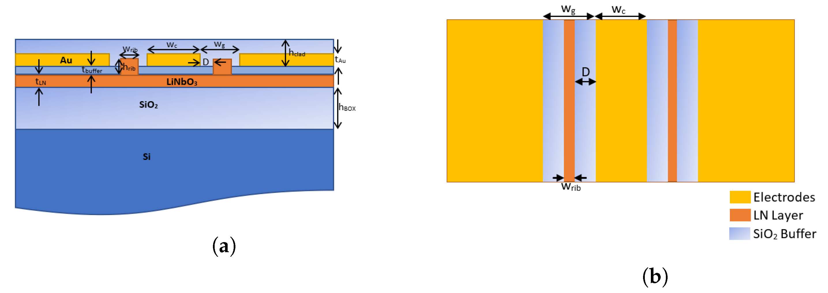
2. Design
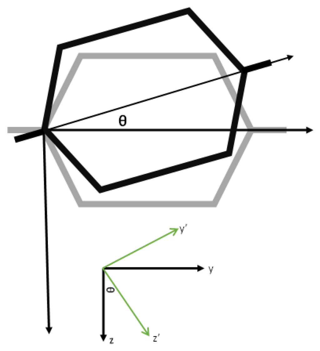
3. Effects of Orientation
4. Distortion Calculation
5. Results and Discussion
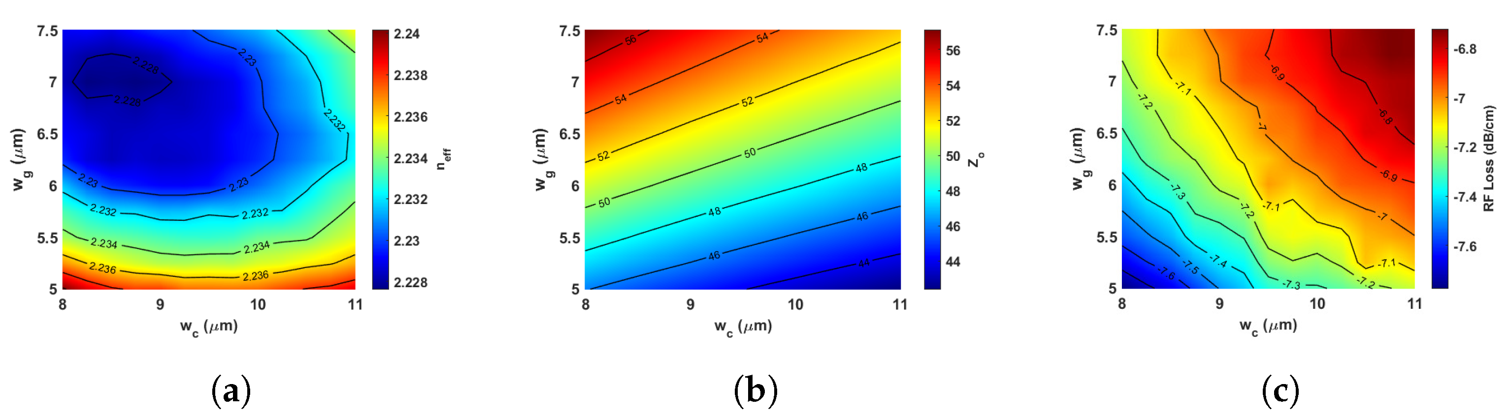
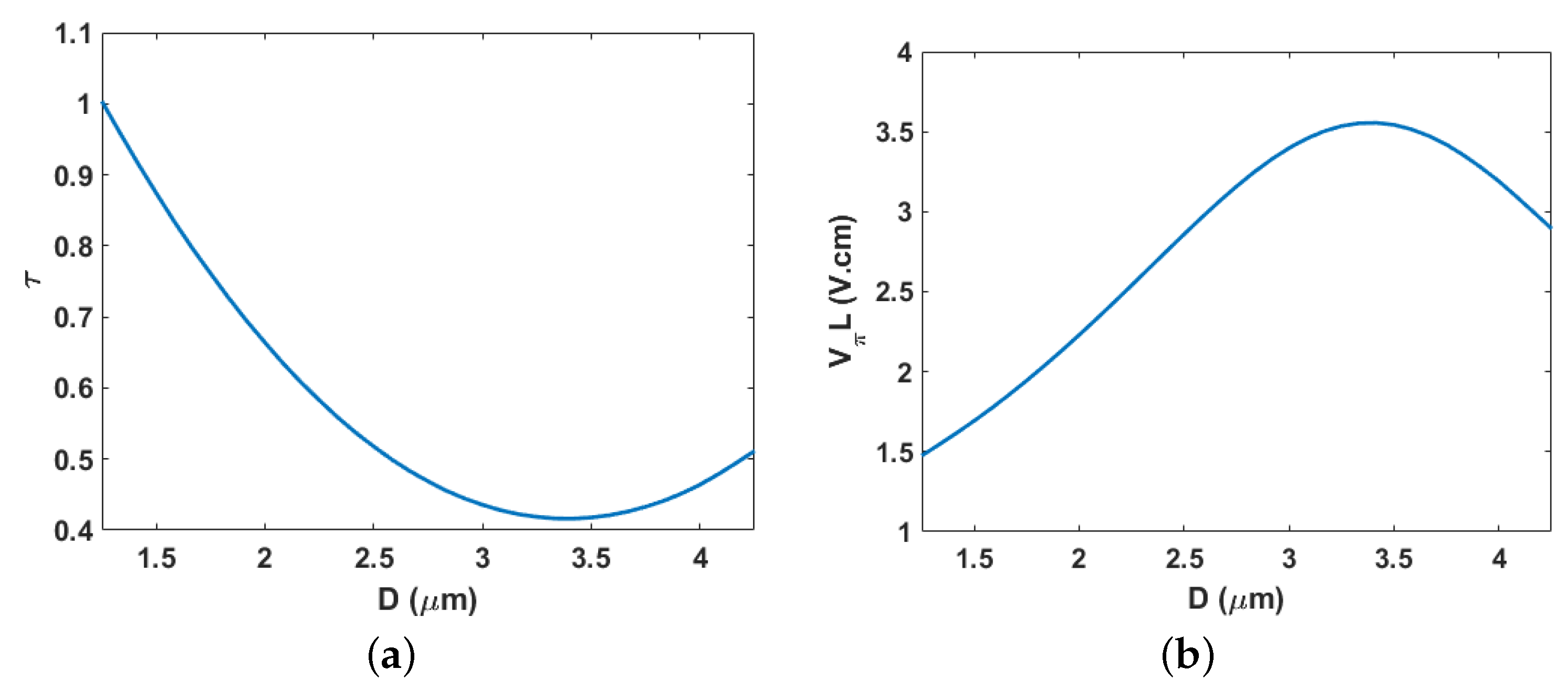
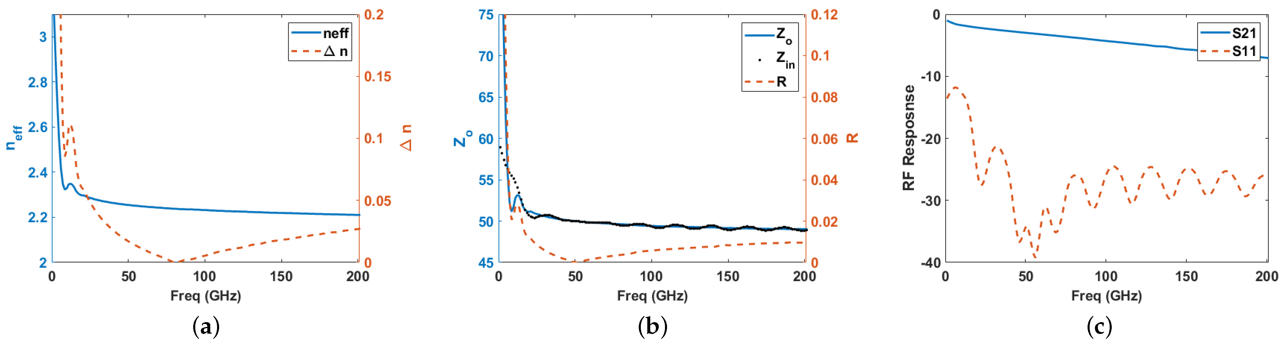
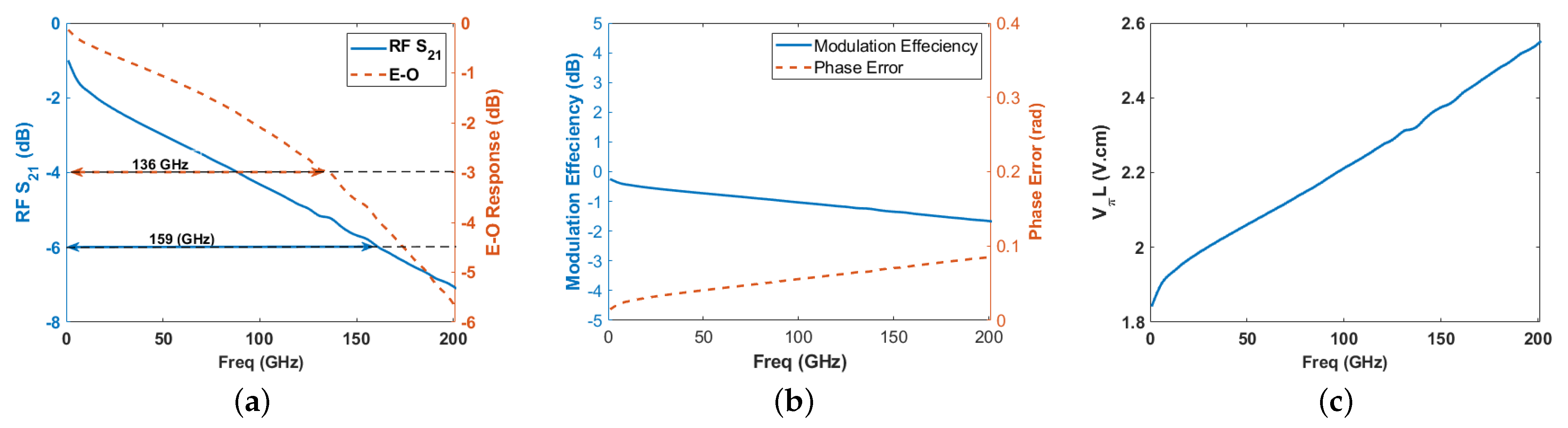
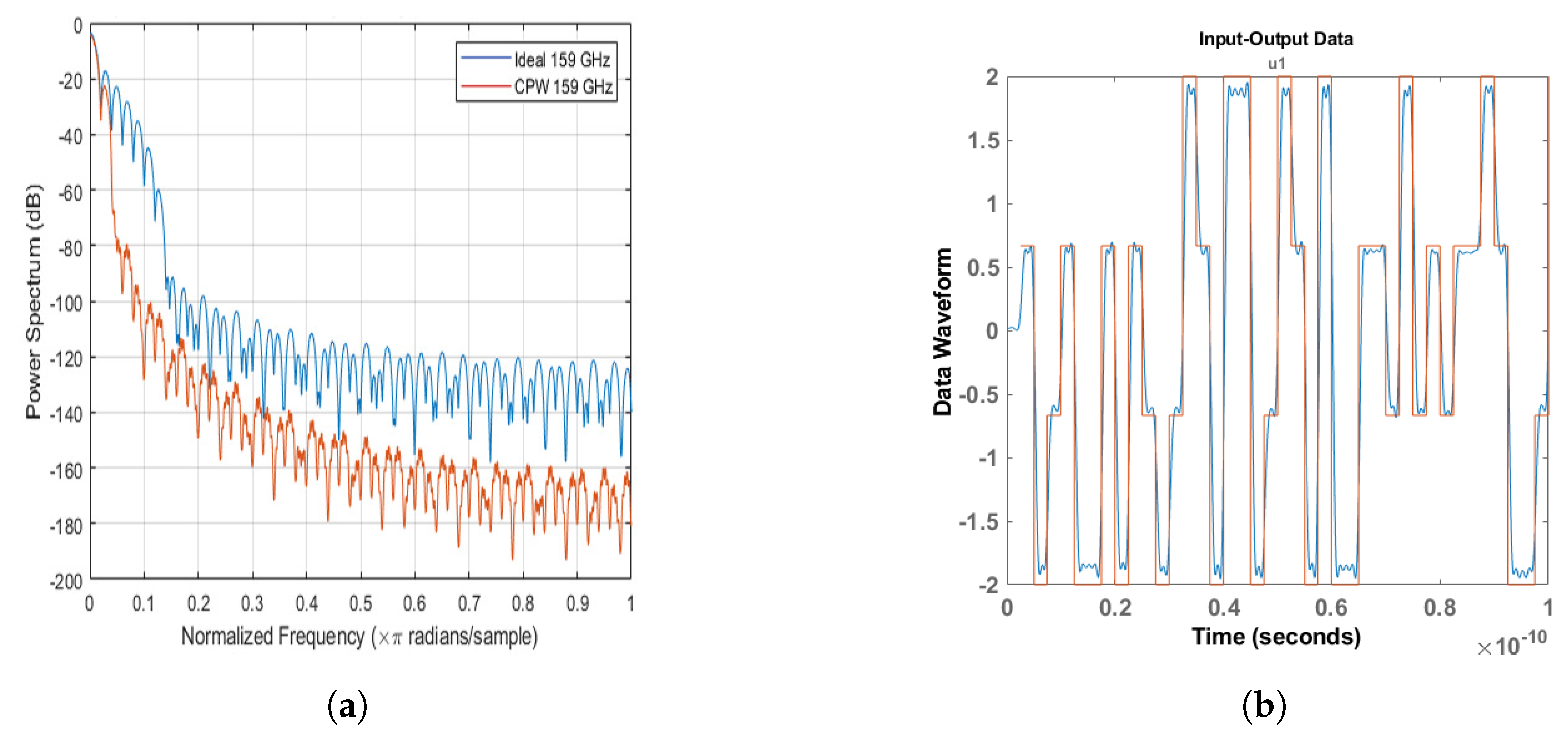
5.1. Electrode Design
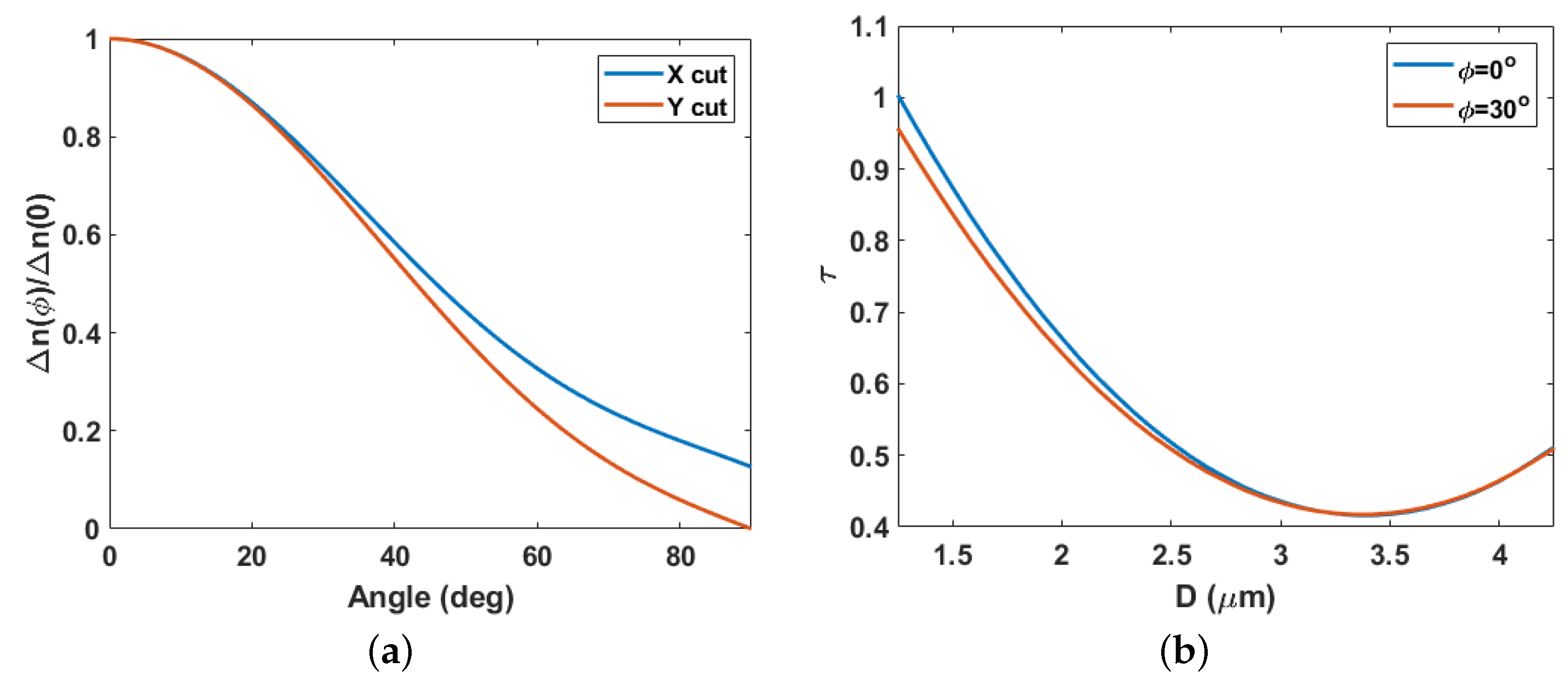
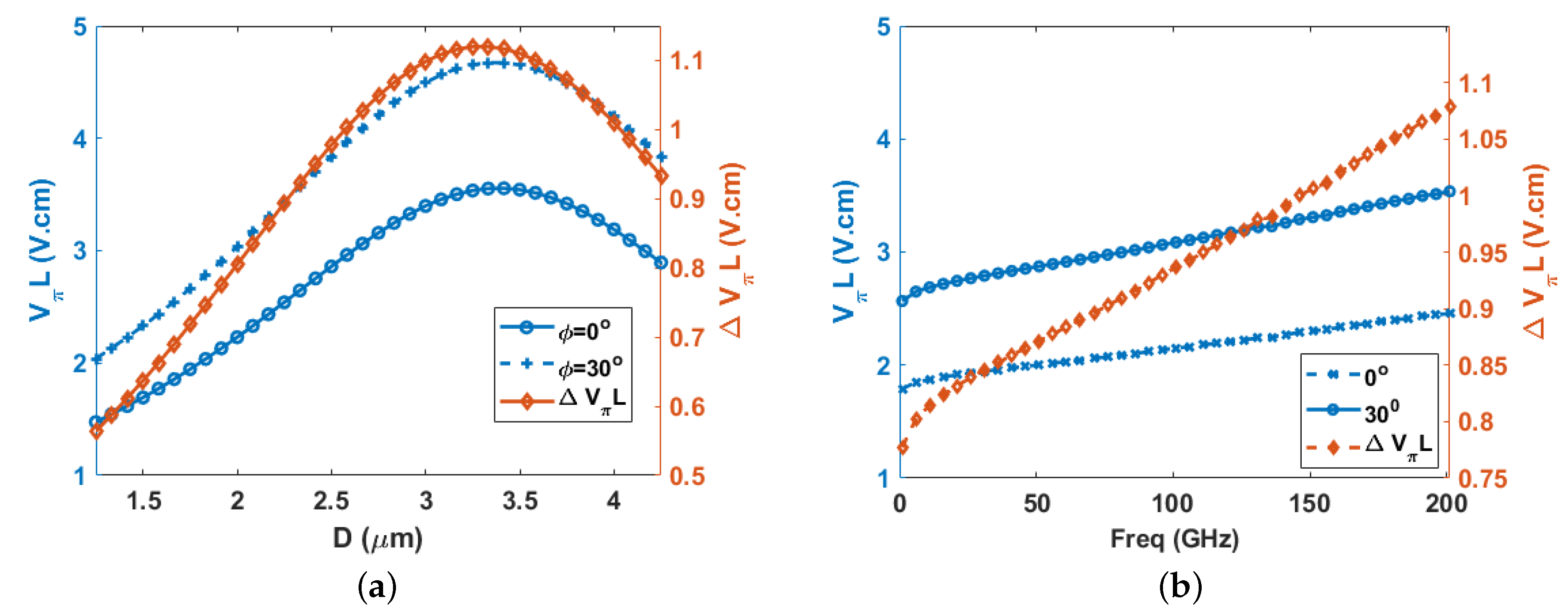
5.2. Orientation
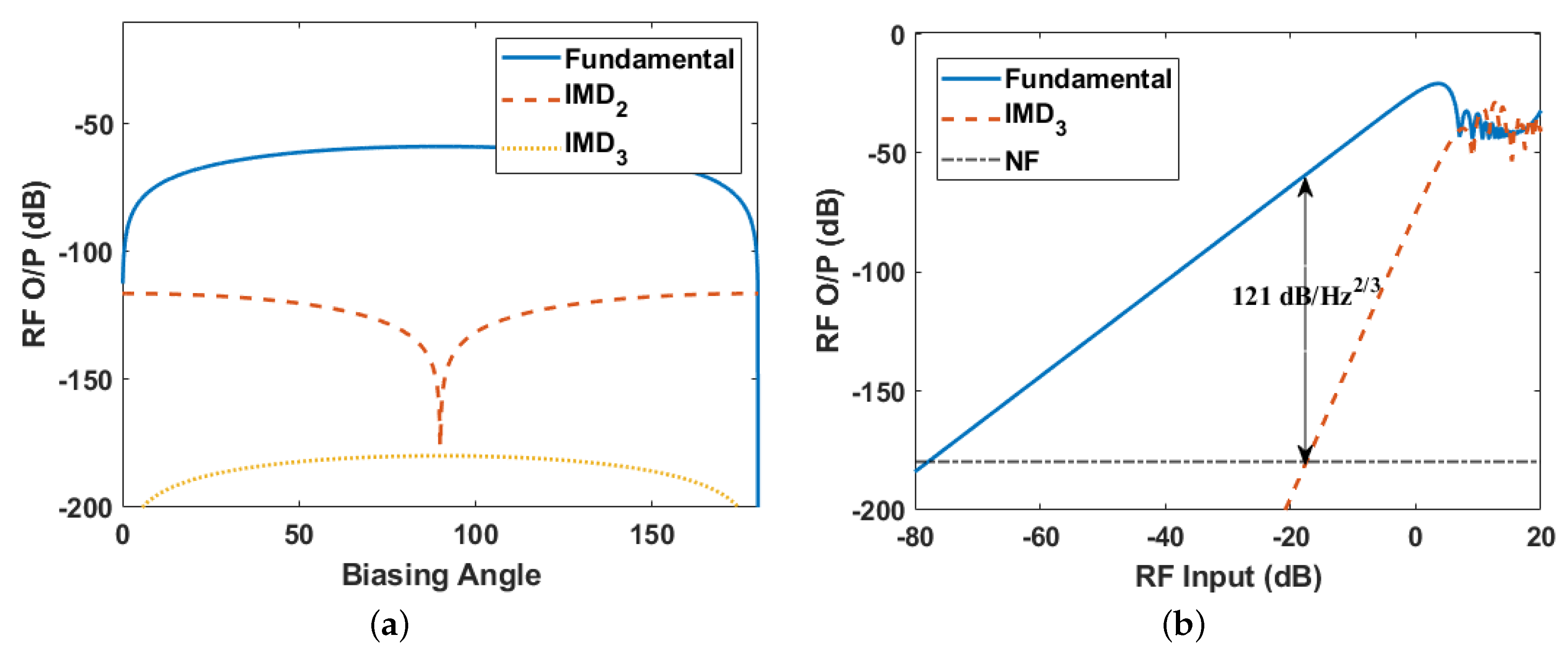
5.3. SFDR Calculation
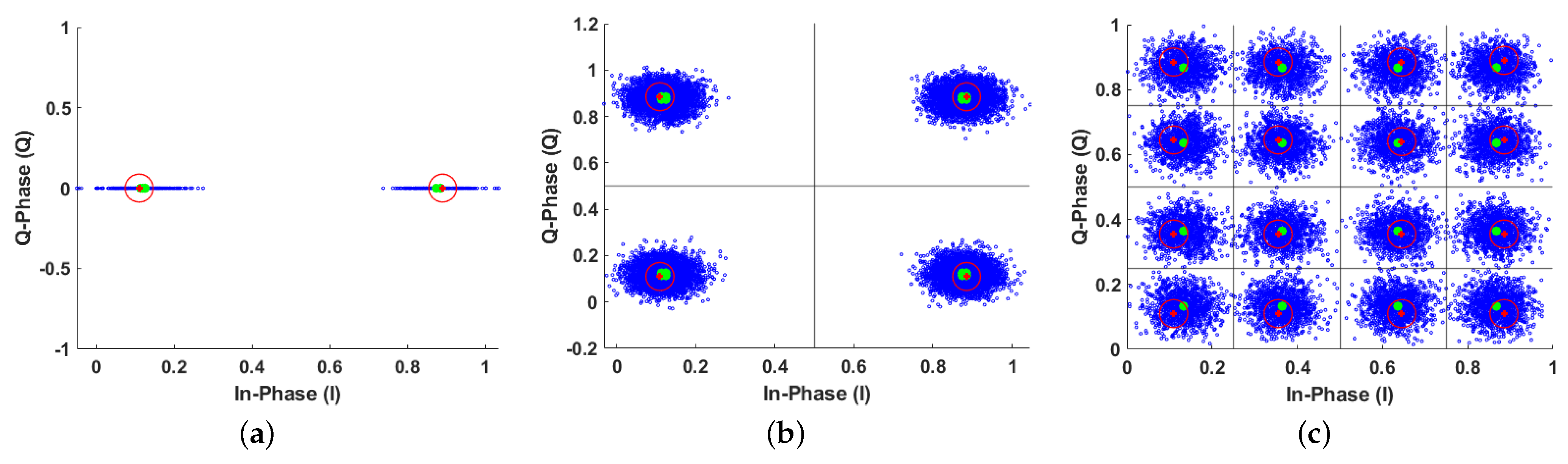
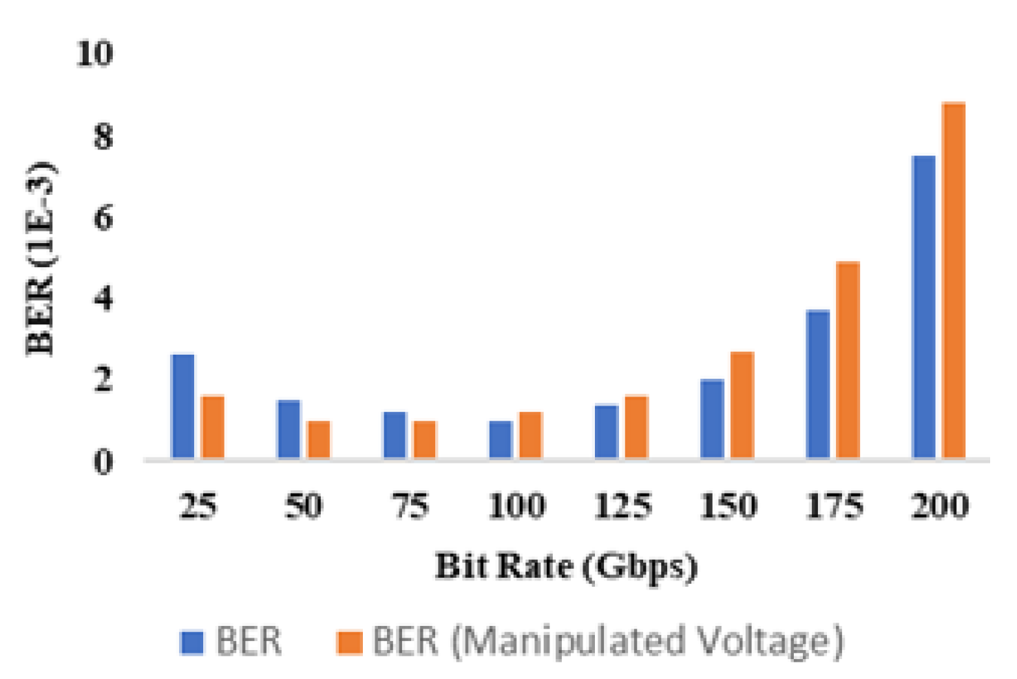
5.4. Digital Modulation Performance
6. Conclusions
Author Contributions
Funding
Institutional Review Board Statement
Informed Consent Statement
Data Availability Statement
Acknowledgments
Conflicts of Interest
Sample Availability
Abbreviations
| EOM | Electrooptic modulator |
| MZI | Mach–Zehnder interferometer |
| SFDR | Spurious free dynamic range |
| PAM | Pulse amplitude modulation |
| QAM | Quadrature amplitude modulation |
| BER | Bit error rate |
| FOM | Figure of merit |
| IMD | Intermodulation distortion |
| TFLN | Thinfilm lithium niobate |
| CPW | Coplanar waveguide |
Appendix A
Appendix A.1. Optimization Method
Appendix A.2. Modulation Efficiency
Appendix A.3. Rotated Coordinates

Appendix A.4. Electrode Filtering Characteristic

References
- Cisco Visual Networking Index: Global Mobile Data Traffic Forecast Update, 2015–2020, 2016, White Paper. Available online: http://www.cisco.com/c/en/us/solutions/collateral/service-provider/visual-networking-index-vnimobile-white-paper-c11-520862.html (accessed on 1 January 2023).
- Zhang, M.; Wang, C.; Kharel, P.; Zhu, D.; Lončar, M. Integrated lithium niobate electro-optic modulators: When performance meets scalability. Optica 2021, 8, 652–667. [Google Scholar] [CrossRef]
- Marpaung, D.; Yao, J.; Capmany, J. Integrated microwave photonics. Nat. Photonics 2019, 13, 80–90. [Google Scholar] [CrossRef] [Green Version]
- Xu, M.; Cai, X. Advances in integrated ultra-wideband electro-optic modulators. Opt. Express 2022, 30, 7253–7274. [Google Scholar] [CrossRef]
- Orlandi, P.; Morichetti, F.; Strain, M.J.; Sorel, M.; Melloni, A.; Bassi, P. Tunable silicon photonics directional coupler driven by a transverse temperature gradient. Opt. Lett. 2013, 38, 863–865. [Google Scholar] [CrossRef] [Green Version]
- Xu, H.; Li, X.; Xiao, X.; Li, Z.; Yu, Y.; Yu, J. Demonstration and Characterization of High-Speed Silicon Depletion-Mode Mach–Zehnder Modulators. IEEE J. Sel. Top. Quantum Electron. 2014, 20, 23–32. [Google Scholar] [CrossRef]
- Errando-Herranz, C.; Takabayashi, A.Y.; Edinger, P.; Sattari, H.; Gylfason, K.B.; Quack, N. MEMS for Photonic Integrated Circuits. IEEE J. Sel. Top. Quantum Electron. 2020, 26, 1–16. [Google Scholar] [CrossRef] [Green Version]
- Zhu, D.; Shao, L.; Yu, M.; Cheng, R.; Desiatov, B.; Xin, C.J.; Hu, Y.; Holzgrafe, J.; Ghosh, S.; Shams-Ansari, A.; et al. Integrated photonics on thin-film lithium niobate. Adv. Opt. Photon. 2021, 13, 242–352. [Google Scholar] [CrossRef]
- Chen, G.; Lin, H.-L.; Ng, J.D.; Danner, A.J. Integrated Electro-Optic Modulator in Z-Cut Lithium Niobate Thin Film with Vertical Structure. IEEE Photonics Technol. Lett. 2021, 33, 1285–1288. [Google Scholar] [CrossRef]
- Sinatkas, G.; Christopoulos, T.; Silipakos, O.; Kriezis, E.E. Electro-optic modulation in integrated photonics. J. Appl. Phys. 2021, 130, 010901. [Google Scholar] [CrossRef]
- Demkov, A.A.; Bajaj, C.; Ekerdt, J.G.; Palmstrøm, C.J.; Ben Yoo, S.J. Materials for emergent silicon-integrated optical computing. J. Appl. Phys. 2021, 130, 070907. [Google Scholar] [CrossRef]
- Honardoost, A.; Safian, R.; Rao, A.; Fathpour, S. High-Speed Modeling of Ultracompact Electrooptic Modulators. J. Light. Technol. 2018, 36, 5893–5902. [Google Scholar] [CrossRef]
- Gopalaknshnan, G.K.; Burns, W.K.; McElhanon, R.W.; Bulmer, C.H.; Greenblatt, A.S. Performance and Modeling of Broadband LiNb03 Traveling Wave Optical Intensity Modulators. J. Light. Technol. 1994, 12, 1807–1819. [Google Scholar] [CrossRef]
- Rao, A.; Patil, A.; Rabiei, P.; Honardoost, A.; DeSalvo, R.; Paolella, A.; Fathpour, S. High-performance and linear thin-film lithium niobate Mach-Zehnder modulators on silicon up to 50 GHz. Opt. Lett. 2016, 41, 5700–5703. [Google Scholar] [CrossRef]
- Betts, G.E. Linearized modulator for suboctave-bandpass optical analog links. IEEE Trans. Microw. Theory Tech. 1994, 42, 2642–2649. [Google Scholar] [CrossRef]
- Mirza, T.N.; Haxha, S.; Dayoub, I. A Linearized Analog Microwave Photonic Link With an Eliminated Even-Order Distortions. IEEE Syst. J. 2021, 15, 4843–4851. [Google Scholar] [CrossRef]
- Shaqiri, S.; Haxha, S.; Flint, I.; Ademgil, H. Microwave photonics analog link based on two integrated D-DPMZM linearized signals and with eliminated odd harmonics and all IMD’s. Opt. Quant. Electron. 2022, 54, 464. [Google Scholar] [CrossRef]
- Wang, C.; Zhang, M.; Chen, X.; Bertrand, M.; Shams-Ansari, A.; Chandrasekhar, S.; Winzer, P.; Lončar, M. Integrated lithium niobate electro-optic modulators operating at CMOS-compatible voltages. Nature 2018, 562, 101–104. [Google Scholar] [CrossRef] [PubMed]
- He, M.; Xu, M.; Ren, Y.; Jian, J.; Ruan, Z.; Xu, Y.; Gao, S.; Sun, S.; Wen, X.; Zhou, L.; et al. High-performance hybrid silicon and lithium niobate Mach–Zehnder modulators for 100 Gbit/s and beyond. Nat. Photonics 2019, 13, 359–364. [Google Scholar] [CrossRef] [Green Version]
- Wang, X.; Weigel, P.O.; Zhao, J.; Ruesing, M.; Mookherjea, S. Achieving beyond-100-GHz large-signal modulation bandwidth in hybrid silicon photonics Mach Zehnder modulators using thin film lithium niobate. APL Photonics 2019, 4, 096101. [Google Scholar] [CrossRef] [Green Version]
- Ahmed, A.N.R.; Shi, S.; Mercante, A.; Nelan, S.; Yao, P.; Prather, D.W. High-efficiency lithium niobate modulator for K band operation. APL Photonics 2020, 5, 091302. [Google Scholar] [CrossRef]
- Liu, Y.; Li, H.; Liu, J.; Tan, S.; Lu, Q.; Guo, W. Low Vπ thin-film lithium niobate modulator fabricated with photolithography. Opt. Express 2021, 29, 6320–6329. [Google Scholar] [CrossRef]
- Huang, X.; Liu, Y.; Li, Z.; Guan, H.; Wei, Q.; Yu, Z.; Li, Z. Advanced Electrode Design for Low-Voltage High-Speed Thin-Film Lithium Niobate Modulators. IEEE Photonics J. 2021, 13, 1–9. [Google Scholar]
- Patel, D.; Ghosh, S.; Chagnon, M.; Samani, A.; Veerasubramanian, V.; Osman, M.; Plant, D.V. Design, analysis, and transmission system performance of a 41 GHz silicon photonic modulator. Opt. Express 2015, 23, 14263–14287. [Google Scholar] [CrossRef] [Green Version]
- Simons, R.N. Coplanar Waveguide Circuits, Components, and Systems; John Wiley and Sons: Hoboken, NJ, USA, 2001. [Google Scholar]
- Chen, E.; Chou, S.Y. Characteristics of Coplanar Transmission Lines on Multilayer Substrates: Modeling and Experiments. IEEE Trans. Microw. Theory Tech. 1997, 45, 939–945. [Google Scholar] [CrossRef] [Green Version]
- Goswami, S.; Thompson, D.; Williams, R.S.; Goswami, S.; Venkatesan, T. Colossal current and voltage tunability in an organic memristor via electrode engineering. Appl. Mater. Today 2020, 19, 100626. [Google Scholar] [CrossRef]
- Hou, Y.; Zhang, X.; Wu, W.; Zhang, T.; Chen, P.; Deng, Z. Controlling the Surface Roughness of Surface-Electrode Ion Trap Based on Micro-Nano Fabrication. Coatings 2021, 11, 406. [Google Scholar] [CrossRef]
- Current-Tuning, C-Band Ultra-Low-Noise Hybrid Laser (Spec Sheet); Thor Labs: Newton, NJ, USA; Available online: https://www.thorlabs.com/newgrouppage9.cfm?objectgroup_id=13653 (accessed on 1 January 2023).
- Winzer, P.J.; Essiambre, R.-J. Advanced Modulation Formats for High-Capacity Optical Transport Networks. J. Light. Technol. 2006, 24, 4711–4728. [Google Scholar] [CrossRef]
- Melikyan, A.; Kaneda, N.; Kim, k.; Baeyens, Y.; Dong, P. Differential Drive I/Q Modulator Based on Silicon Photonic Electro-Absorption Modulators. J. Lightwave Technol. 2020, 38, 2872–2876. [Google Scholar] [CrossRef]


| 0.3 m | 0.4 m | 1.25 m | 0.2 m | 0.5 m | 2.75 m | 4.7 m | 500 m |
Disclaimer/Publisher’s Note: The statements, opinions and data contained in all publications are solely those of the individual author(s) and contributor(s) and not of MDPI and/or the editor(s). MDPI and/or the editor(s) disclaim responsibility for any injury to people or property resulting from any ideas, methods, instructions or products referred to in the content. |
© 2023 by the authors. Licensee MDPI, Basel, Switzerland. This article is an open access article distributed under the terms and conditions of the Creative Commons Attribution (CC BY) license (https://creativecommons.org/licenses/by/4.0/).
Share and Cite
Gaur, T.; Mishra, P.; Hegde, G.; Srinivas, T. Modeling and Analysis of Device Orientation, Analog and Digital Performance of Electrode Design for High Speed Electro-Optic Modulator. Photonics 2023, 10, 301. https://doi.org/10.3390/photonics10030301
Gaur T, Mishra P, Hegde G, Srinivas T. Modeling and Analysis of Device Orientation, Analog and Digital Performance of Electrode Design for High Speed Electro-Optic Modulator. Photonics. 2023; 10(3):301. https://doi.org/10.3390/photonics10030301
Chicago/Turabian StyleGaur, Tushar, Pragya Mishra, Gopalkrishna Hegde, and Talabattula Srinivas. 2023. "Modeling and Analysis of Device Orientation, Analog and Digital Performance of Electrode Design for High Speed Electro-Optic Modulator" Photonics 10, no. 3: 301. https://doi.org/10.3390/photonics10030301