1. Introduction
Since their advent, semiconductor lasers operating at 650 nm have been widely used in the field of optical data storage and as laser display systems, industrial lasers, and medical equipment due to their advantages in terms of power conversion efficiency and flexible range of wavelength emission [
1]. Nevertheless, the fundamental structure of edge-emitting laser (EEL) diodes results in a poor appearance in lateral optical mode confinement, evidenced by a promiscuous beam on the output facet which reduces the quality of the laser output and affects the further application of the device [
2]. Therefore, optimizing the devices’ electro-optical conversion efficiency with a good lateral fundamental mode purity is one of the hot spots in academic research and the industrial field.
According to the fundamental structure of EEL, the higher-order optical modes, which are distributed on both sides of the waveguides, can oscillate easily and then affect the far-field pattern (FFP) of the laser beam [
3]. To suppress the high-order mode, microstructures beside the ridge aim to stabilize the fundamental mode oscillation and increase the oscillation threshold of the higher-order optical mode [
4]. In 2016, a ridge-edge-emitting laser with an asymmetric waveguide and isolated double-trench was designed by the Beijing University of Technology. This laser obtained a low-threshold 852 nm laser with a single fundamental mode. This work studied the influence of the ridge parameters of the depth to width ratio on the lateral mode characteristics [
5].
In this work, a mode-modulation design was investigated theoretically and experimentally to achieve an ideal far-field beam quality. After analyzing the distribution of the current and optical mode of each order, obtained through simulations, we fabricated an EEL chip with a deep trench on the gentle side of the ridge waveguide. By causing a refractive index change in the waveguide structure, these trenches lead to the additional loss of higher-order side optical mode and keep the high-order optical mode from emitting. Additionally, these trench designs are beneficial for preventing current diffusion and increasing the optical confinement factor [
6].
2. Process and Simulation
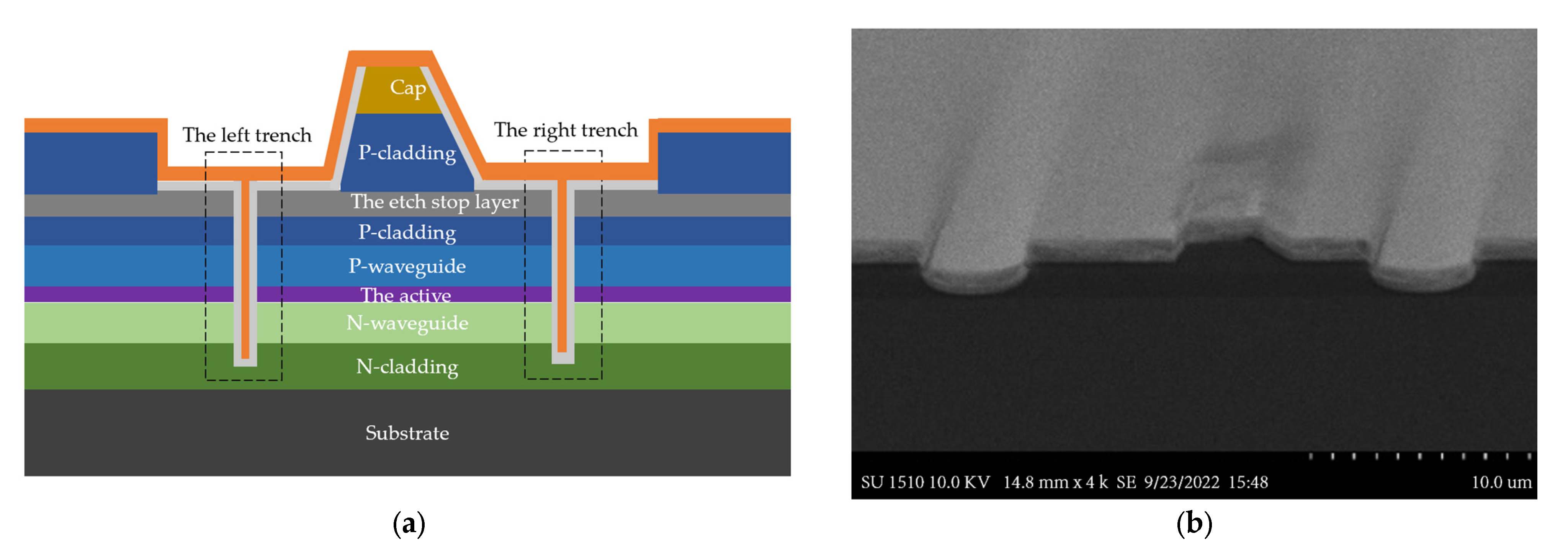
The laser structure was grown using metal–organic vapor phase epitaxy (MOVPE) in an Aixtron reactor. The epitaxial structure is provided in
Table 1. The layers were deposited on (100) GaAs substrates with a 15° offcut towards the (111) A-direction. A 200 nm thick GaAs was first grown to isolate the defects of the substrate. The tensile-strained, GaInP, dual-quantum well was embedded with an AlGaInP barrier. A 100 nm AlGaInP-waveguide layer was then embedded on both sides of the active layer. The N-cladding was made from AlInP with Si doping, and the P-cladding was made from magnesium-doped AlInP [
7]. The designed chip is shown in
Figure 1a. The ridges were defined in a photoresist using standard, i-line contact lithography, then formed by wet etching. The etching depth of the ridge was controlled well by an additional etch-stop layer (ESL) in the P-cladding structure, a SEM photo of which is shown in
Figure 1b. The ridge was perpendicular to the cavity surface (110).
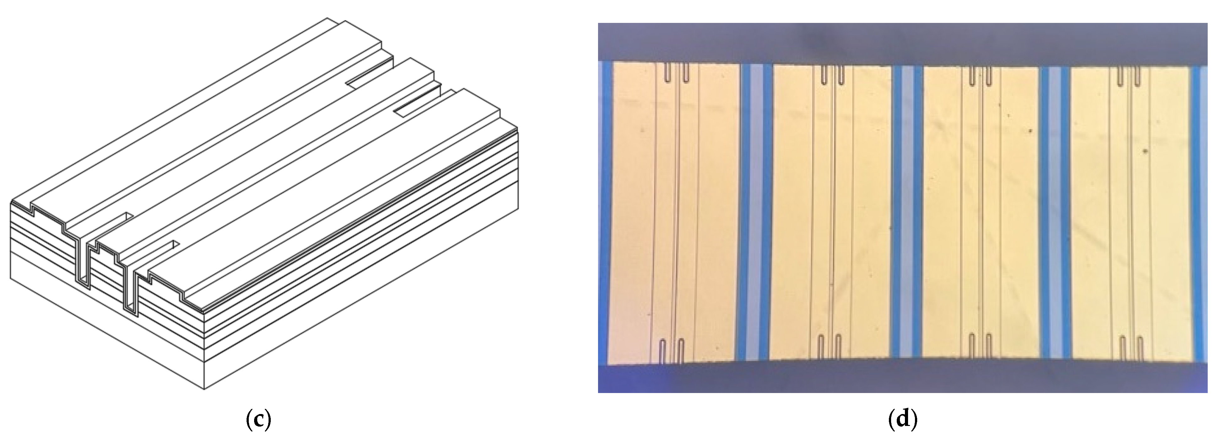
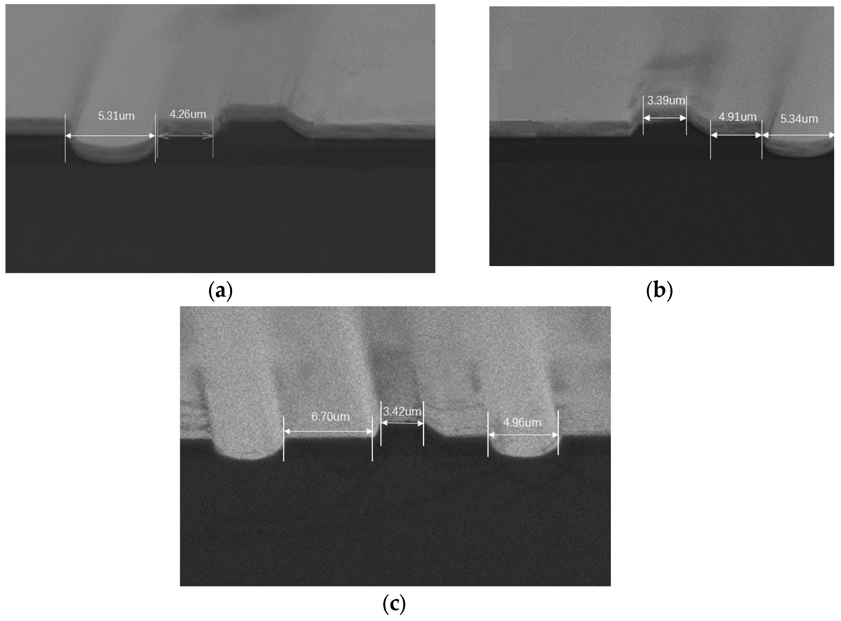
After the ridge was etched, the trench was made with photolithography using wet etching to transfer the design onto the wafer, which was controlled well by the etching time to ensure the depth and width. A 200 nm thick silicon dioxide insulating layer was deposited using plasma-enhanced chemical vapor deposition (PECVD), and a contact window was defined on top of the ridge waveguide. A thick gold p-contact was applied to allow for p-side-down mounting. After fabricating the laser structure, the substrate was thinned to 100 um by a chemical–mechanical polishing (CMP) thinning process on the n-contact side of substrate wafer. The device was then cleaved to a total length of 350 um. The mode-modulation laser structure with narrow trenches on the sides of the ridge of the waveguide is shown in
Figure 1c, and the trench is etched into the N-doped cladding layer. Finally, the appearance of the bar is shown in
Figure 1d. The depth of the prepared trench was 2500 nm.
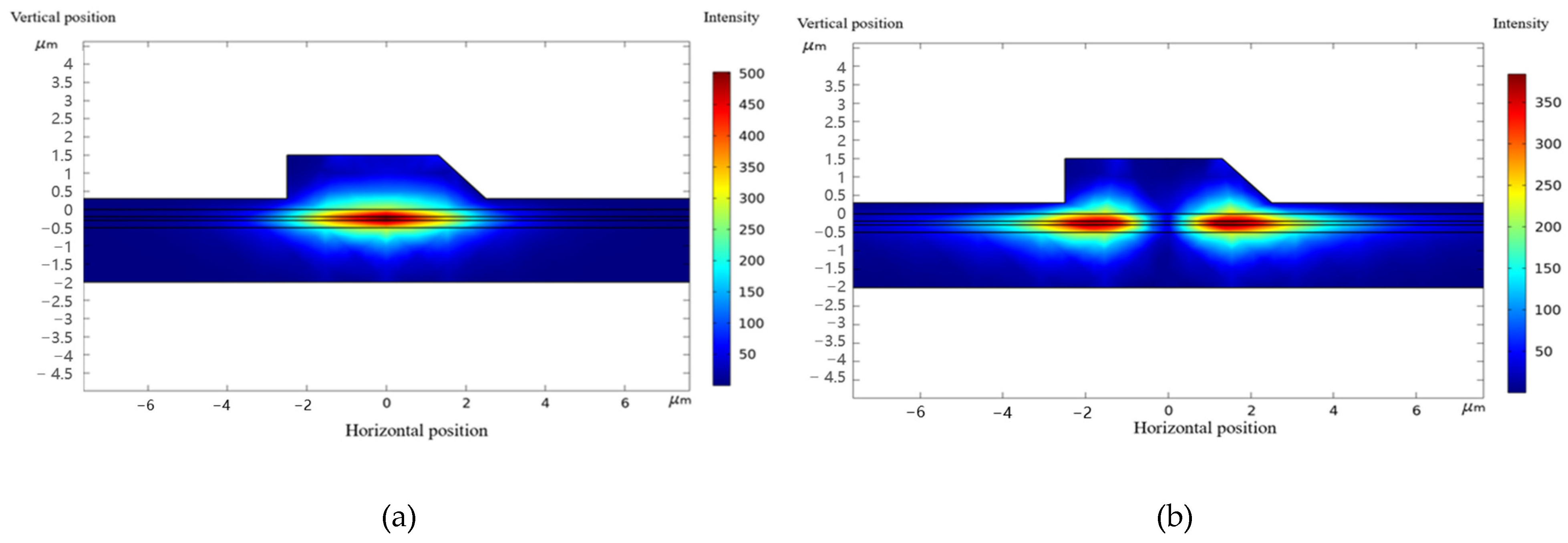
To investigate the mode distribution in the ridge waveguide structure, we used the finite element simulation software COMSOL Multiphysics to calculate the laser operation mode and cavity-surface optical field distribution. According to the simulations illustrated in
Figure 2, there were mainly two optical mode distributions in the semiconductor laser with a 5 um wide ridge waveguide: the fundamental optical mode and the second-order optical mode. The maximum intensity of the fundamental mode is usually localized at the active region below the ridge waveguide and shifts toward the sides, whereas the second-order optical mode is divided into two energy peaks and similarly extends over the sides [
8].
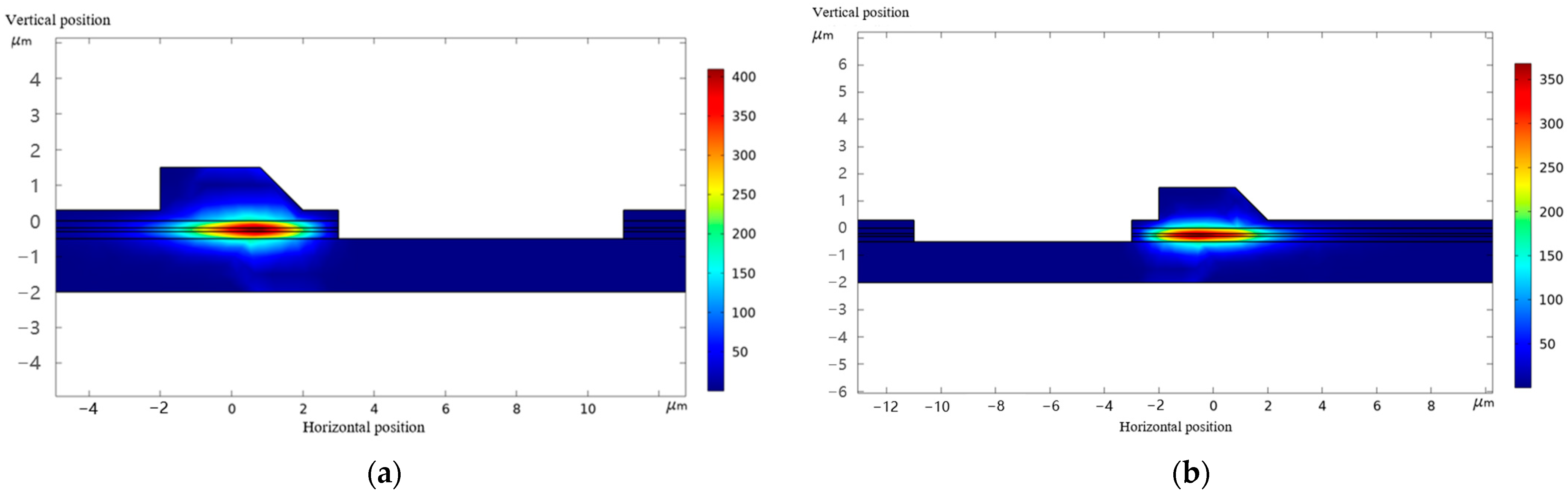
When bilateral trenches were added to the EEL, as shown in
Figure 3, the first-order mode was suppressed, and there was only the fundamental mode in the active region below the ridge waveguide. However, the maximum intensity of the fundamental mode field was much lower than those without trenches. We believe this was caused by the additional loss of trenches beside the laser ridge, which effected the laser oscillation.
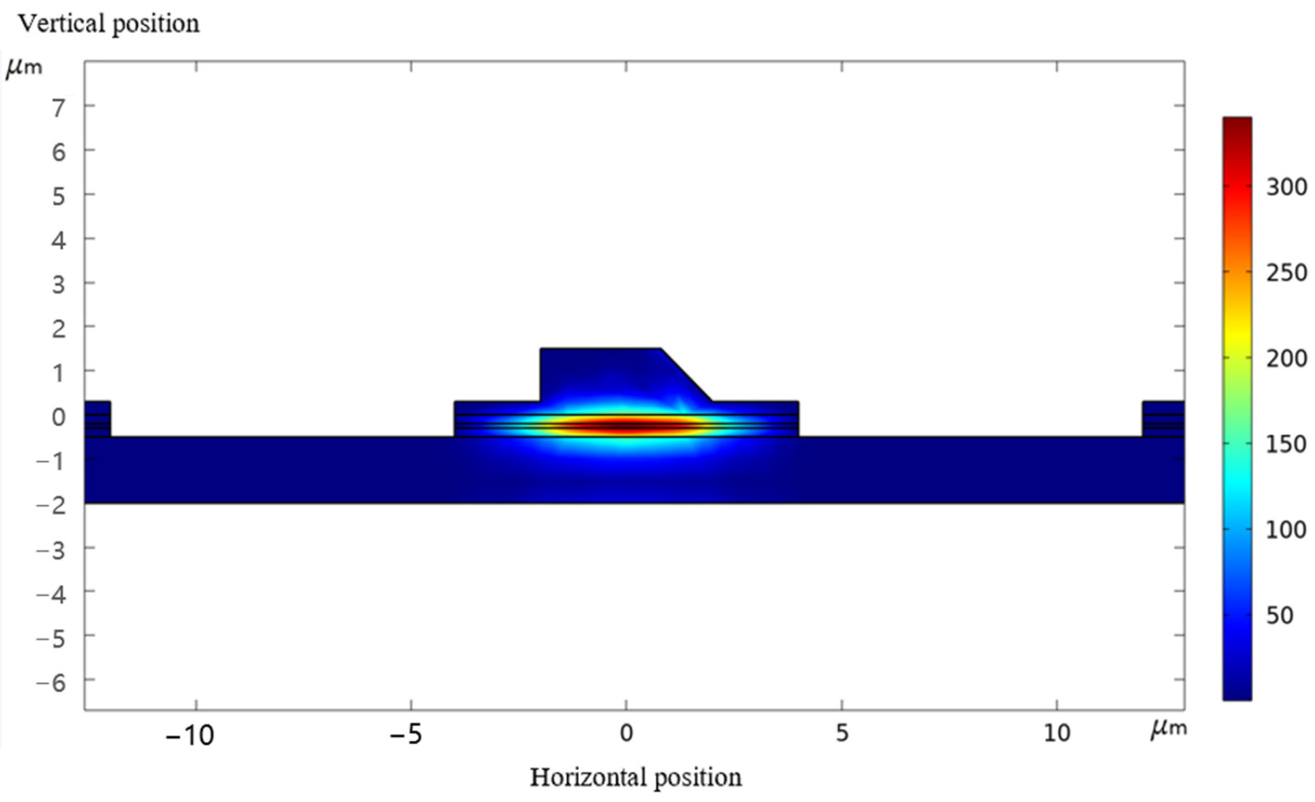
Figure 4a,b show a single trench structure on the left and right side, respectively. It can be seen that, similar to the bilateral trenches, with a proper distance, the first-order mode was also suppressed by trench. However, the mode field intensity of the trench structure on right side of the ridge was higher than the left trench structure. We believe this was because the effective index and current expansion blocking ability were higher on the gentle side. The added trench on the gentle side, with a wider ridge area to expand the current and enlarge the mode gain area, could provide a better optical confinement ability.
The threshold gain theory of LDs can be expressed as:
where
represents the factor of threshold gain,
represents the internal loss,
L represents the cavity length, and
R represents the cavity surface reflectivity. With the same
L and
R, the threshold gain,
, of the laser mode can be increased by adding the internal loss,
. To make the fundamental mode emit easily and maintain the output power, the internal loss,
should be designed precisely. The higher internal loss of the higher-order optical modes compared to the fundamental mode will isolate the emission of the higher-order modes and achieve the purpose of optimizing the lateral beam quality [
9].
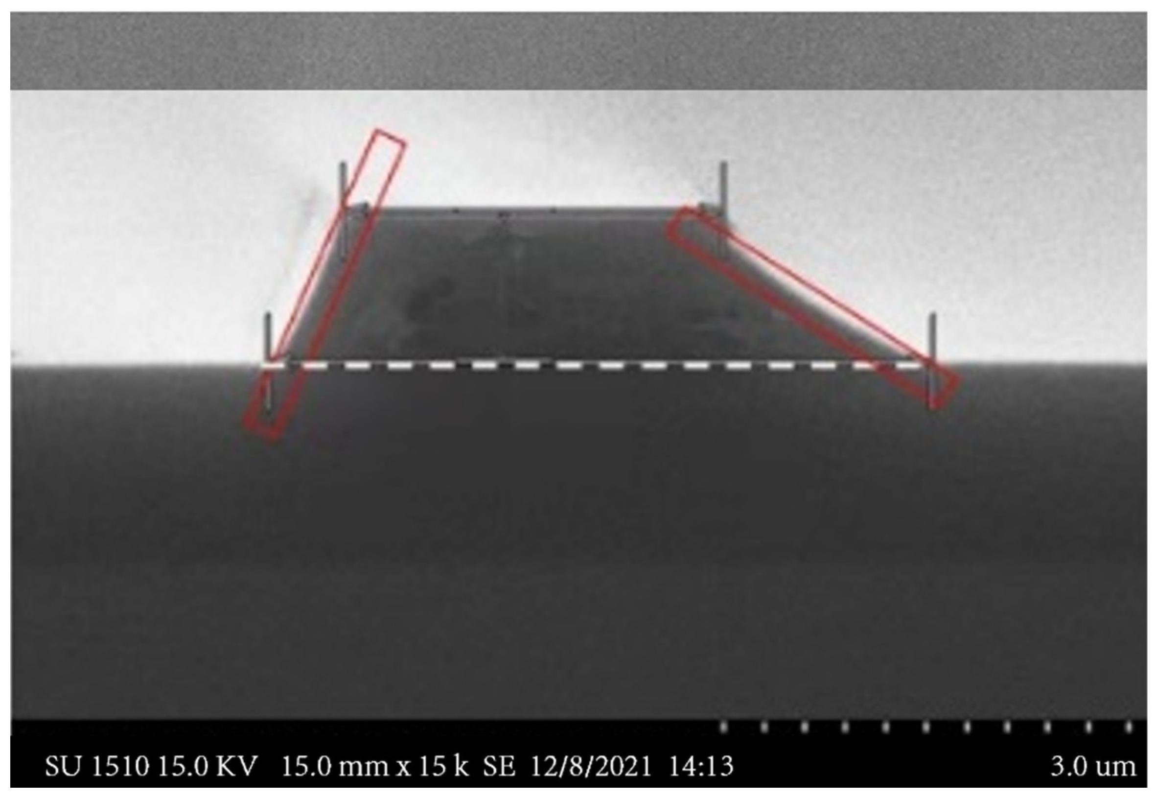
The appearance of the ridge is shown in
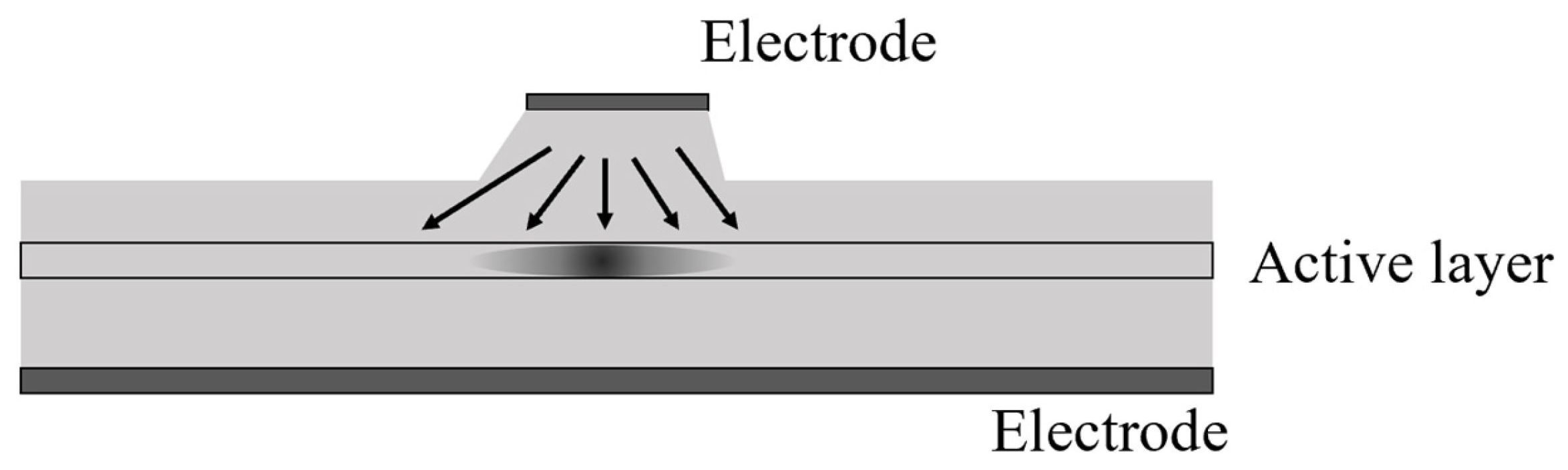
Figure 5. The anisotropy of the materials in the wet etching process leads to the asymmetric ridge structure. The gentle side (in the right trench structure) is 31°, while the steep side (in the left trench structure) is 53°. The asymmetric ridge influences the current diffusion, as shown in
Figure 6, leading to more gain-area expansion and a severe beam filament phenomenon on the gentle side [
10,
11]. In order to explore the impact of this asymmetry, three different designs of the mode-modulation trench, the left trench structure (near steep slope), the right trench structure (near the gentle slope), and the bilateral trench structure, shown in
Figure 7, were fabricated and investigated, respectively.
3. Results
The chips were tested on a needle probe platform.
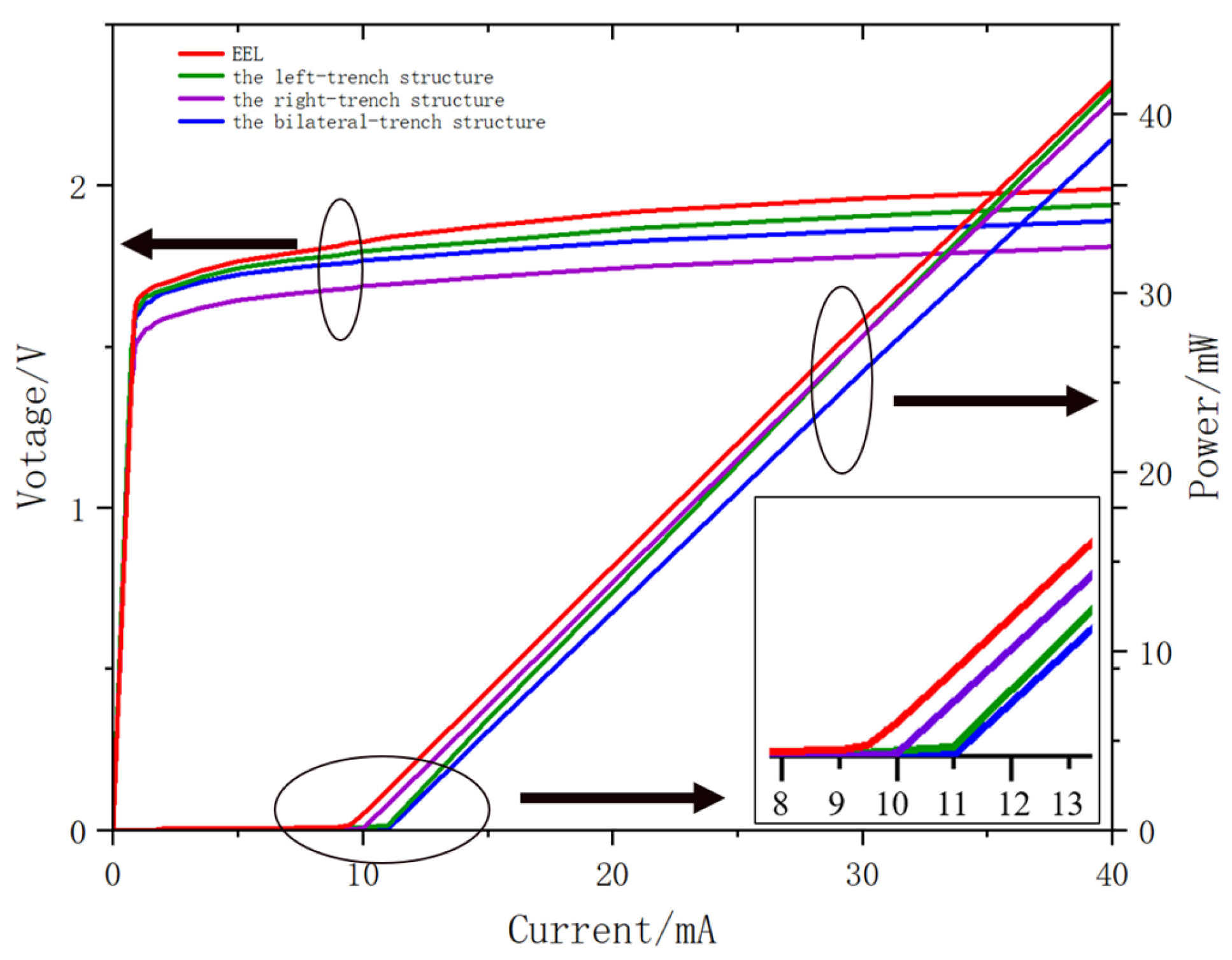
Figure 8 shows the output power and voltage against current characteristics measured, ranging from 0 to 40 mA. The blue curve in
Figure 8 belongs to the bilateral trench structure, and the threshold current and voltage were 11.1 mA and 1.89 V, respectively. For an operating current of 40 mA, the output power went as high as 38.6 mW, and an electro-optical conversion efficiency of 50% is demonstrated with a slope efficiency of 1.3 W/A. For the purple curve obtained upon the max injection current of 40 mA with the right trench structure, the threshold current and voltage were 10.3 mA and 1.81 V, respectively, the highest output power and slope efficiency were 40.8 mW and 1.32 W/A, respectively, and the electro-optical conversion efficiency was 56%. The green curve is represents the left trench structure, which demonstrated a threshold current and voltage of 11.3 mA and 1.94 V, respectively, a highest output power and slope efficiency of 41.5 mW and 1.39 W/A, respectively, and an electro-optical conversion efficiency of 53%. The red curve in the comparison belongs to the EEL, and the threshold current and voltage were 9.2 mA and 1.99 V, respectively, and the highest output power and slope efficiency were 42 mW and 1.35 W/A, respectively.
The record value for the maximum output power achieved by the lasers with the left trench groove structure was 6.99% higher than that of the bilateral trench structure. Additionally, the output power of the right trench structure demonstrated a 5.39% higher value than the bilateral trench structure. The low output power of the bilateral trench structure is the reason for the high-mode loss and even damage to the fundamental mode. It is illustrated by the high threshold current of the bilateral trench structure. The high output power and low threshold current of the EEL also illustrate this point. It should be noted that the slightly larger voltage difference of Curve II is may be due to poor contact.
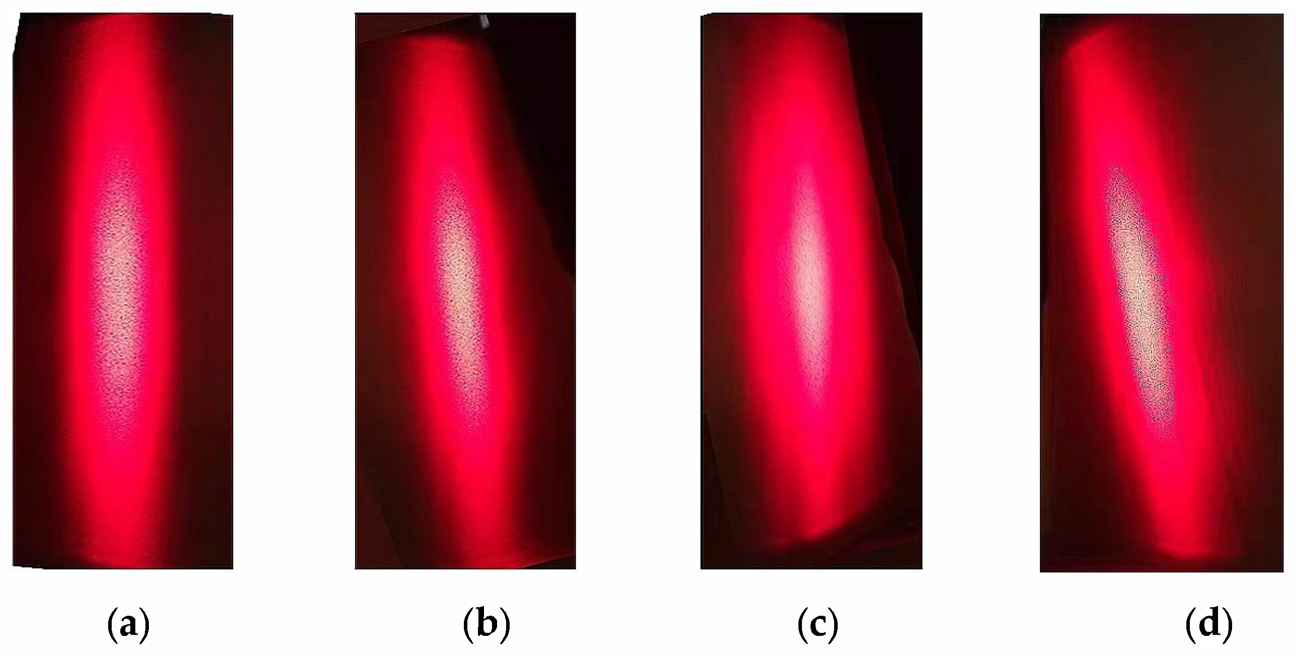
The FFP image of the lasers, illustrated in
Figure 9, was created by taking images on the screen at fixed positions. The test current was 40 mA. The laser beam image in
Figure 9a is of the bilateral trench structure, demonstrating a regular oval shape with a clear edge without blurring. The laser beam image in
Figure 9b is of the right trench structure, with an oval shape and no filiform at the edges. The laser beam image in
Figure 9c,d are the left trench structure and the EEL, the edge of which is unrecognizable and demonstrates multiple vertical filiformes on both sides. The main difference between
Figure 9a–d is whether a filiform exists on both sides. This demonstrates that the gain of the low-order mode also reached the lasing condition, which is reflected by the filiformes.
From the above results, it can be observed that the high-mode suppression effect of the bilateral- trench and the right trench structures were better than that of the left-trench structure. This is because, on the gently sloping side, the trench can more effectively block the current lateral diffusion. The mode competition and the modal gain are reduced in the cavity, which is also be very useful in suppressing undesirable effects in laser diodes [
12,
13].
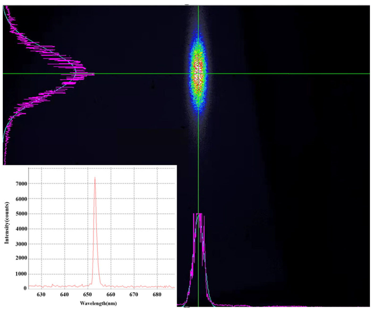
In order to characterize the beam quality of the right trench structure, a CCD camera beam-analyzing system was used to record and plot the beam intensity with an injection current of 40 mA. The measured far-field spot is shown in
Figure 10. It can be seen that the center intensity of the elliptical beam is strong, and the two curves exhibit Gaussian distribution. The typical spectrum of a 653 nm diode laser at an operating current of 40 mA is also shown in the insert image of
Figure 10.
4. Conclusions
In this paper, we developed a mode-modulated structure of a ridge waveguide laser which suppresses the current diffusion and increases the diffraction loss of the high-order side modes. By increasing the threshold difference between the fundamental and higher-order side modes, we achieved higher-order side-mode suppression and minimized the beam “splitting” phenomenon. By comparing the output characteristics of the three different mode-modulated structures, the output power of the right trench structure and the left trench structure are greater than that of the bilateral trench structure. Further, a better beam quality was realized in the right trench structure than the left trench structure. Finally, we developed a new ridge waveguide laser structure with a single trench on the gently sloping side. At an input current of 0.04 A, the chip output power is 40.8 mW, the slope efficiency is 1.32 W/A, the electro-optical conversion efficiency is 56%, and the horizontal beam divergence angle is 17°.

 ,
, 


