Article

A Design of All-Optical Integrated Linearized Modulator Based on Asymmetric Mach-Zehnder Modulator

1
State Key Laboratory on Integrated Optoelectronics, Institute of Semiconductors, Chinese Academy of Sciences, Beijing 100083, China
2
College of Materials Science and Opto-Electronic Technology, University of Chinese Academy of Sciences, Beijing 100049, China
*
Author to whom correspondence should be addressed.
Photonics 2023, 10(3), 229; https://doi.org/10.3390/photonics10030229
Submission received: 28 January 2023 / Revised: 14 February 2023 / Accepted: 19 February 2023 / Published: 21 February 2023

Abstract

:
We proposed an all-optical linearized modulator model suitable for an integration platform. The linearized modulator is formed by an asymmetric Mach–Zehnder modulator and a carrier-separated waveguide. We focus on the suppression of both intermodulation distortion (IMD3) and second-order harmonic distortions (SHD). As a result, the third-order nonlinear terms of IMD3 and second-order nonlinear terms of SHD are entirely suppressed, leading to a spurious free dynamic range of IMD3 (SFDRIMD3) improvement of ~14 dB and SFDRSHD improvement of ~3 dB compared with a standard MZM model. The influence of large RF input signals, losses, and fabrication deviations are also discussed to prove the feasibility of the model.

1. Introduction

Microwave photonics (MWP) has received extensive attention in recent years with the advantages of both the microwave and the photonics fields [1,2,3]. Modern MWP links have become increasingly crucial as higher-order QAM coherent systems become more analog-like and require a higher linear transmitter [4]. Prevalent microwave photonic links employ a direct detection (DD) scheme in which Mach–Zehnder modulators (MZMs) are widely used. However, the sinusoidal transmission characteristics of the MZM are the main limiting factor in the linearity of the MWP links, which restricts the spurious free dynamic range (SFDR). Therefore, it is highly desirable to develop a high-linearity modulator to propel the development of MWP systems.
Many MZM linearization methods have been suggested and implemented, which can be broadly categorized as electrical, mixed, and all-optical. Electrical linearization can achieve ultra-high SFDR at low frequency, but the bandwidth is limited by the speed of electronic processing [5,6,7,8]. The third-order nonlinearity is eliminated in silicon modulators built in a regular MZM configuration by optimizing doping [9]. However, this is not applicable to material platforms with a linear electro-optic effect. The mixed linearized modulator typically uses a dual-parallel Mach–Zehnder modulator (DPMZM) [10,11,12,13] to produce complimentary third-order intermodulation distortion (IMD3), as it cancels the IMD3 at the detector. However, a mixed linearized modulator requires precise control of the optical power splitter ratio, broadband microwave attenuator, and phase shifter. All-optical linearization includes discrete links and integrated modulators. The discrete all-optical linearization is ultra-wideband and wavelength-independent, but it requires an attenuator to eliminate the IMD3, which causes unwanted signal attenuation [14]. The integrated linearized modulators mainly utilize a micro-ring [15,16,17,18,19,20,21] or Bragg grating [22] to improve the interference characteristic of the Mach–Zehnder interferometers (MZIs), which have been successfully implemented on the Silicon Photonics platform. These integrated modulators are attractive for their simplicity and robustness, but the resonators limit the bandwidth.
In this paper, we propose an all-optical linearization design for the integrated modulator. The linearized modulator is formed by an asymmetric Mach–Zehnder modulator and a carrier-separated waveguide, called carrier separated asymmetric Mach–Zehnder modulator (CS-AMZM). A mathematical model is built to investigate the linearity of the CS-AMZM structure. The second-order harmonic distortions (SHDs) and IMD3 can be suppressed simultaneously at a specific operating point to achieve a spurious-free status within the full operating broadband. At the same time, CS-AMZM does not contain resonators, so its operating bandwidth can be close to MZM. Through calculation and simulation, the SFDRSHD of CS-AMZM is close to MZM, and the SFDRIMD3 is ~14 dB higher than the standard MZM. In the case of large input power, the harmonics can be further suppressed by feedback control. In addition, after considering the leading design and process errors in fabrication, it is revealed that the performance is almost consistent with the ideal case except for loss.

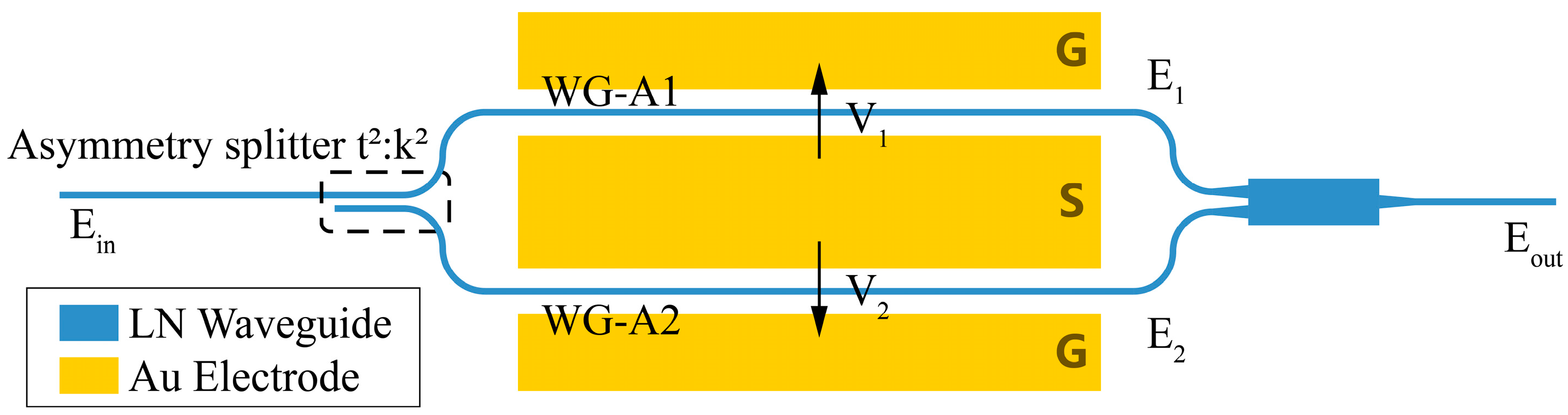
2. Linearized CS-AMZM Model

The nonlinearity effect of a modulator is usually represented by the two-tone test. The modulator is driven by two signals whose frequencies are closely spaced. Because of the nonlinear electro-optic response of the modulator, the output optical signal contains new frequency components called intermodulation distortions (IMDs) and harmonic distortions (HDs). The nonlinearity calculation usually only considers the IMD3 but ignores the SHD, which limits the system within the range of the sub-octave bandwidth. To improve the system’s performance, the SHD is also a factor that must be considered. Therefore, the SHD and IMD3 need to be suppressed simultaneously, and the loss of (first-order harmonics) FH components should also be minimized.
We first consider the ideal model of an AMZM, as shown in Figure 1. The difference between AMZM and MZM is that the power ratio of the input beam splitter is unequal. Directional coupler splitter (DCS), 1 × 2 MZI, asymmetric Y branch, and arbitrary ratio MMI [23,24,25] are all suitable choices for asymmetric beam splitters. In this paper, DCS is chosen for calculation and design. The power ratio of the splitter is t2: k2, and of course, t2 + k2 = 1. The input optical field of the AMZM is Ein = E0exp(jωt), and the driving signals of the two arms (WG-A1 and WG-A2) consist of a two-tone signal and a direct current bias, written as:
V 1 = V D C + v 0 cos ω 1 t + cos ω 2 t V 2 = v 0 cos ω 1 t + cos ω 2 t ,
where v0 is the amplitude of the RF signal and VDC is the direct current bias voltage. ω1 and ω2 are the angular frequencies of the two-tone signal. Here, to simplify the calculation, we let DC voltage only exist in the upper arm, which does not affect the correctness of the calculation. The phase difference between WG-A1 and WG-A2 caused by the DCS can be ignored owing to VDC, which can achieve any desired operating points. Therefore, VDC will directly represent the phase difference between WG-A1 and WG-A2. The modulated optical field of the two arms can be written as:
E 1 = E 0 t exp j ω t + x D C + x 0 cos ω 1 t + cos ω 2 t E 2 = E 0 k exp j ω t x 0 cos ω 1 t + cos ω 2 t ,
where x0 = πv0/Vπ and xDC = πVDC/Vπ are the modulator index of the RF signal and DC bias, respectively. Vπ is the half-wave voltage of the AMZM. We normalize E0 to 1 and set the operating point of AMZM to exp(jxDC) = j. In addition, only linear electro-optic materials are considered here, such as lithium niobate (LN). The modulation of voltage to phase is linear and ignores asymmetries of WG-A1 and WG-A2. The modulation sidebands are calculated using Bessel expansion. Following this, the coefficients of the sidebands related to the FH, SHD, and IMD3 in the Eout can be written as:
0 :   W 0 = 1 2 j t + k J 0 2 ± ω 1 , ± ω 2 :   W 1 = 1 2 t + j k J 0 J 1 ± 2 ω 1 , ± 2 ω 2 :   W 2 = 1 2 j t + k J 0 J 2 ± ω 1 ω 2 :   W 11 = 1 2 j t + k J 1 2 ± 2 ω 1 ω 2 , ± 2 ω 2 ω 1 :   W 21 = 1 2 t + j k J 1 J 2 ,
where Wi is the power of the corresponding sideband. Jn is a simplified form of Jn(x0), which is the n-order Bessel function of the first kind, and [±ωi] represents exp(jωt ± jωit). For square-law detectors, the photocurrent of the FH, SHD, and IMD3 components can be calculated by the modulation sidebands (see Appendix A):
I F H W 0 W 1 * + W 1 W 0 * = t k J 0 3 J 1 1 2 t k x 0 I S H D 2 W 0 W 2 * + W 2 W 0 * + W 1 W 1 * + W 1 W 1 * = t 2 + k 2 1 2 J 0 2 J 1 2 J 0 3 J 2 0 I I M D 3 W 0 W 21 * + W 21 W 0 * + W 1 W 11 * + W 11 W 1 * + W 1 W 2 * + W 2 W 1 * = t k J 0 2 J 1 J 2 + 1 2 J 0 J 1 3 1 8 t k x 0 3 ,
where the Bessel function is approximated by a power series expansion under the case of the small signal; it can be seen in Equation (4) that for AMZM, although the SHD is almost nonexistent, neither FH nor IMD3 have zero points. If a cancellation component can be introduced, the FH and IMD3 components can obtain different zero points. Therefore, a carrier-separated AMZM (CS-AMZM) is proposed, as seen in Figure 2.
For IMD3 components to obtain zero points, we add an adjustable 1 × 2 splitter to separate a portion of the carrier, whose power ratio is p2: q2, p2 + q2 = 1. The arm for the separated carrier, called WG-CS, has a heating electrode to control the phase shift, which is defined as Δϕ. It should be noted that the adjustable 1 × 2 splitter will introduce a phase difference of π on the two arms. Δϕ includes this phase difference, and represents the total phase difference between the two output ports. The optical field of WG-A1, WG-A2, and the WG-CS can be written as:
E 1 = p t exp j x D C exp j ω t + j x 0 cos ω 1 t + cos ω 2 t E 2 = p k exp j ω t j x 0 cos ω 1 t + cos ω 2 t E 3 = q exp j Δ ϕ ,
The photocurrent of the FH, SHD, and IMD3 components can be written as
I F H 1 2 p 2 p k t + 2 q t cos Δ ϕ + k sin Δ ϕ x 0 I S H D 2 4 p q k cos Δ ϕ + t sin Δ ϕ x 0 2 I I M D 3 1 64 p 8 p t k + 2 q k cos Δ ϕ + t sin Δ ϕ x 0 3 ,
It can be seen in Equation (6) that, after separating the carrier, the SHD and IMD3 components can exist with different zero points with a suitable Δϕ.
Figure 3 shows the IFH, ISHD, and IIMD3 in Equation (6) changed with the power ratio of the two splitters when Δϕ = 7/8π. The zero points of SHD and IMD3 components are marked with a dotted black line and solid black line, respectively. x0 is set to 0.001, which is small enough to satisfy small-signal conditions. It should be noted that as for t, p = 0, or 1, CS-AMZM equivalents to a phase modulator, a waveguide, or a single AMZM, so the ranges of t2 and p2 are limited from 0.001 to 0.999. It can be seen that the variation in SHD is independent of t2. SHD and IMD3 have a unique common zero point. Since Figure 3 will change with Δϕ, in order to find the maximum value of FH, we performed the calculation for different Δϕs.
The common zero point of SHD and IMD3 changes as Δϕ changes, as shown in Figure 4a. When Δϕ is in a specific range, SHD and IMD3 have a common zero point. It is independent of p to suppress SHD for a certain Δϕ. Therefore, t can be fixed with a specific splitter structure. The FH power reaches its maximum when Δϕ = 7.6/8π, as shown in Figure 4b. In actual fabrication, it is difficult to make a waveguide with fixed phase-shifting due to the inaccurate length and width. Therefore, a more practical approach is to use thermo-optic or electro-optic effects to make adjustable phase shifters. The advantage of the adjustable phase shifters is that the fabrication error of t can be adjusted by Δϕ. Hence in actual fabrication, the power of FH depends on t. The effective interval for t2 is (0.6, 1). In this interval the suppression of SHD and IMD3 will not be affected, but only the power of FH will be affected. This is a relatively sufficient tolerance; simple process design is required to ensure that t2 is in this interval. We can set an adjustable t2 to maximize the power of FH. However, because t2 and Δϕ affect each other, if both parameters are adjustable, the device will be more unstable. When the environment or experimental conditions change, it is necessary to adjust the two parameters at the same time to make them match each other, which increases the difficulty of adjustment. For such comprehensive considerations, we recommend fixing t2.

3. Results and Discussion

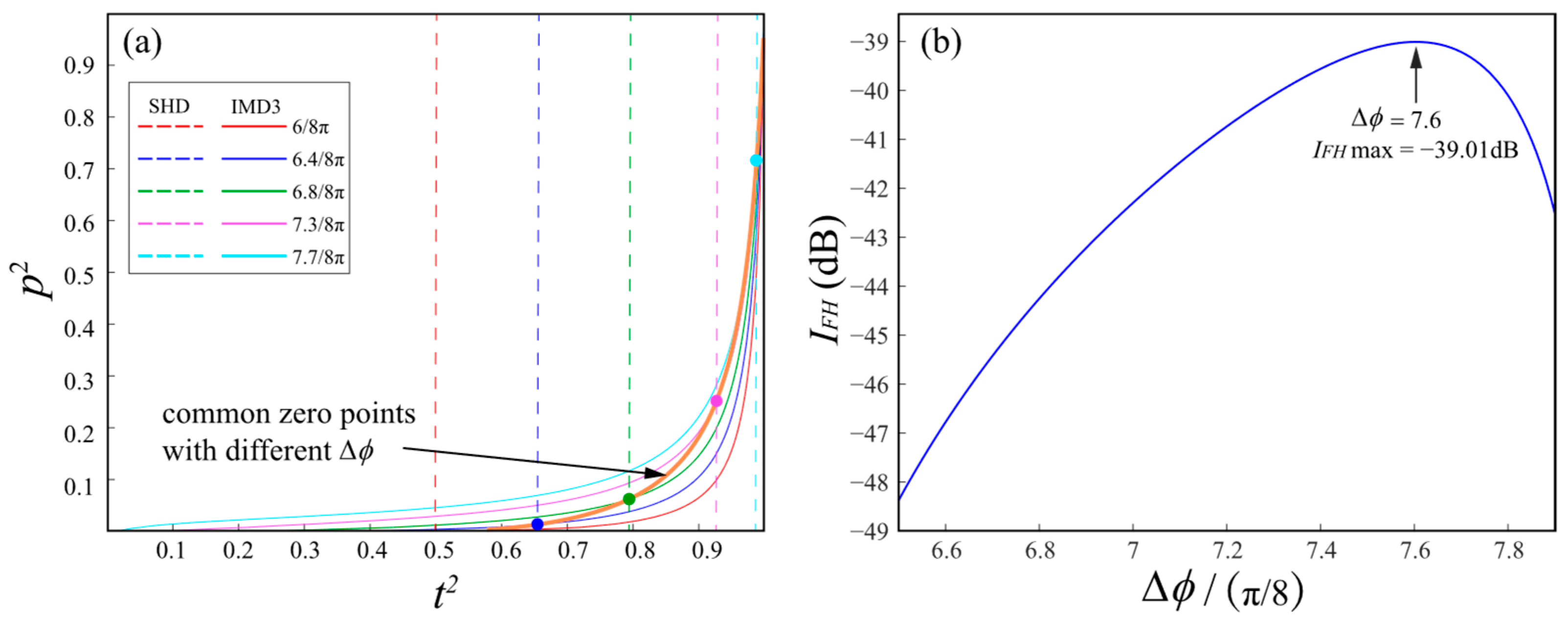
3.1. Ideal CS-AMZM Simulation

In this section, the CS-AMZM was analyzed under ideal conditions. We used Lumerical INTERCONNECT to simulate the proposed CS-AMZM. Following this, CS-AMZM is compared with a standard MZM under the same conditions. The device parameters in the simulation are shown in Table 1, and the simulation settings are shown in Table 2. The test link of CS-AMZM is shown in Figure 5.
In the simulation, the solver settings are default, and losses are not considered, and the phase differences among WG-A1, WG-A2, and WG-CS are not considered. The linear operating point of the CS-AMZM is the same as calculated in the previous section. Δϕ is set to 7.6/8π, corresponding to achieving the common zero points of SHD and IMD3. The RF input power is 7 dBm. The frequency of the two-tone signal is set to 10 GHz and 11.25 GHz. We disabled the thermal noise of the laser and detector to detect the harmonics with eminently low power. This only eliminates white noise, which does not affect harmonic generation. Meanwhile, we adjusted the sensitivity of the RF spectrum analyzer to −200 dBm. When calculating SFDR, the NF is set to −162 dBm/Hz, which can be obtained in the experiment [15].
I T H , 3 1 96 p 8 p t k + 2 q k cos Δ ϕ + t sin Δ ϕ x 0 3 ,
The TH and IMD3 components have the same zero points. In the 5-octave range, the harmonics and intermodulation of the signal will be much lower than that of MZM and other linearized modulators, which do not consider SHD cancellation.
Simulated SFDR results of the standard MZM and the proposed CS-AMZM are shown in Figure 6c. Compared with MZM, although the FH power of the CS-AMZM is reduced, the SFDRIMD3 is improved by 14 dB, and the SFDRSHD is improved by 2.8 dB due to the complete suppression of harmonics. We note that the slopes of IMD3 power versus input power is ~5 for the CS-AMZM, because we have almost completely suppressed the third-order nonlinear components under small-signal conditions. Therefore, the main component of IMD3 is fifth-order nonlinear components. The fifth-order nonlinear component of IMD3 is calculated as (see Appendix B):
I I M D 3 , 5 p 2 t k 2 J 0 J 1 J 2 2 + 2 J 0 J 1 2 J 3 + J 1 3 J 2 ,
Fifth-order nonlinear components are not affected by separated carriers and have no zero points, which defines the linearization limit of CS-AMZM.
We performed a tolerance analysis of p2 and Δϕ with an RF input power of 10 dBm, as shown in Figure 7. The influence of p2 offset on each component is given in Figure 7a, which shows that p2 has little influence on FH and SHD. As mentioned in 3.2 in the manuscript, for large input signals, the minimum power of IMD3 is not at the optimal linear point, and the increase in IMD3 is less than 10dB when the offset of p2 is between −0.004 and 0.008. Figure 7b shows the effect of the offset of Δϕ on each component. It can be seen that a slight change in Δϕ leads to a large increase in SHD. Therefore, in practical application, the accuracy and stability of Δϕ should be ensured first, to obtain higher SFDRSHD. If only IMD3 needs to be suppressed, the accuracy requirements for both p2 and Δϕ are drastically reduced.

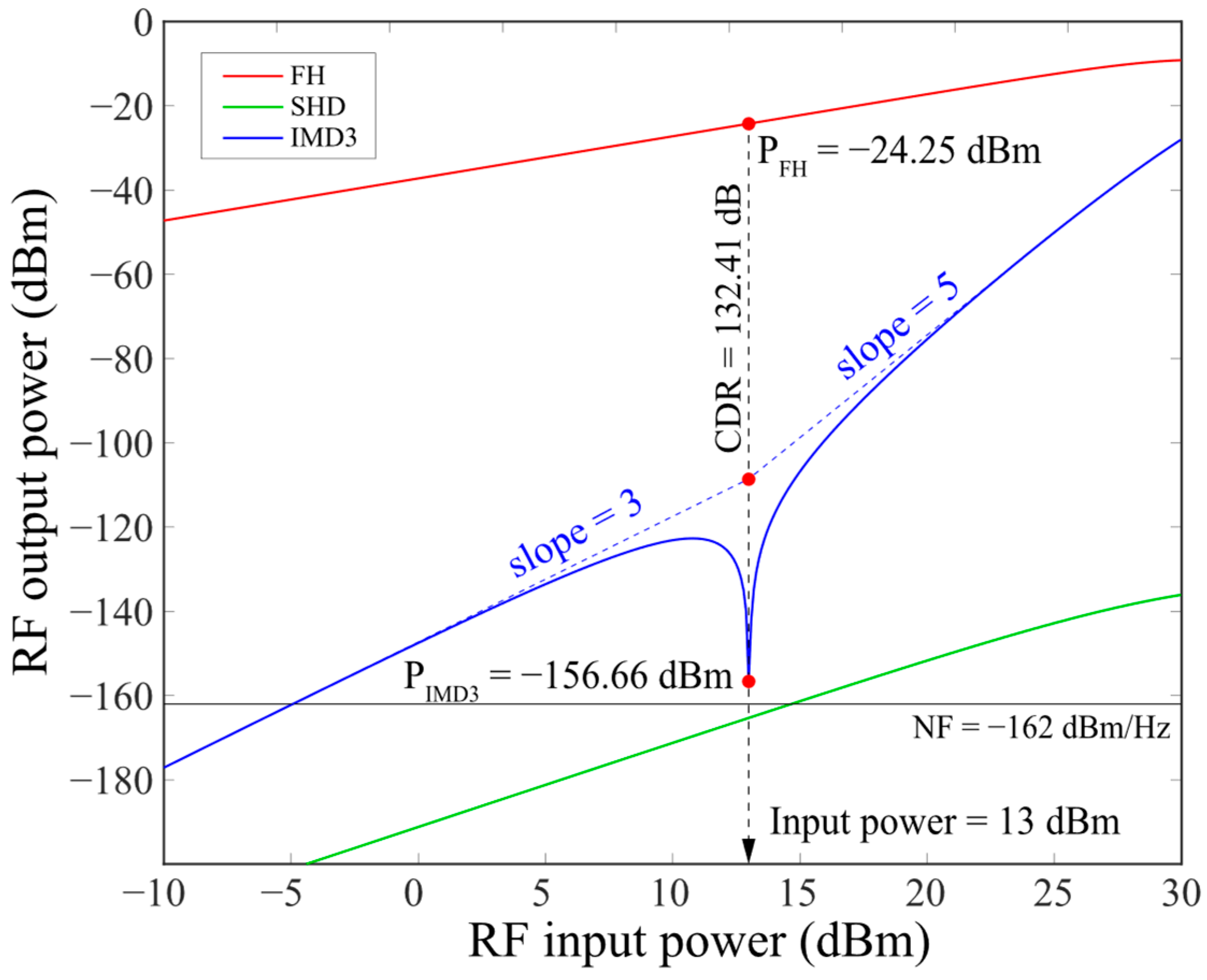
3.2. The Case of Large RF Input Power

As shown in the dashed line in Figure 6c, Bessel expansion does not satisfy linear approximation at large-signal conditions, and the beat higher-order nonlinear components cannot be neglected. In order to perform the calculation for the large-signal case, we abandon the approximation of the Bessel function and add the fifth-order beat frequency components in IMD3 (see Equation (8)). The normalized photocurrent under a small-signal condition (x0 = 0.001) and large-signal condition (x0 = 1) is shown in Figure 8. The zero points are shifted in the large-signal condition for both FH and IMD3 components. The zero points of the SHD are almost constant.
The linearization condition is t2 = 0.976 and p2 = 0.550 when the input power is 13 dBm. The input power is scanned under this condition, and the result is shown in Figure 9. The input power corresponding to the position of the notch is exactly the input power. The slope is three for less than the input power and five for more. IMD3 contains all nonlinear components of an odd order. Higher-order nonlinear components have lower power. When the operating point slightly deviates from the condition of complete suppression of the third-order nonlinear components, the power of the third-order and fifth-order components are close. Therefore, the IMD3 for small input power is dominated by the third-order nonlinear components, while the IMD3 for large input power is dominated by the fifth-order nonlinear components. The intersection of the two extension lines is the position of the notch. In this case, the third- and fifth-order nonlinear components are almost equal. It can be seen from Equations (6) and (8) that the third- and fifth-order components are inverted. They are almost entirely canceled out when the power is equal, forming the notch.
This phenomenon means that intermodulation distortions can be further suppressed at large signals by improving the feedback-control system. If a fixed control point is used, a high SFDR can be obtained. If adaptive control of the smallest harmonics can be achieved, an operating point with the minimum IMD3 power can be found by adjusting p2 under large signals. Consequently, the modulator’s carrier-to-distortion ratio (CDR) under large signals can be significantly improved.

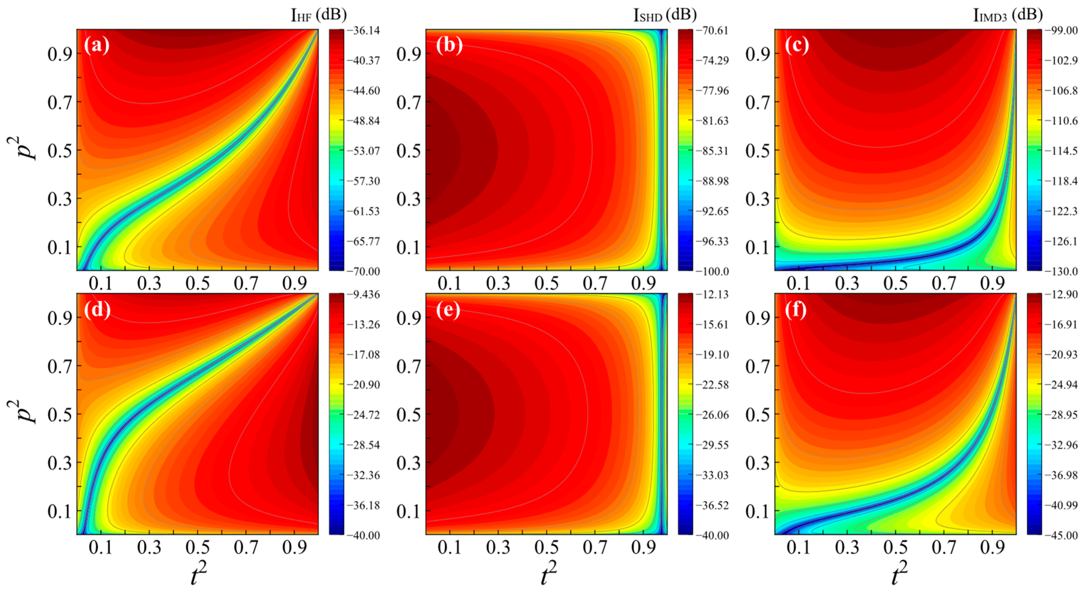
3.3. Influence of Losses and Fabrication Deviations

The losses and deviations in fabrication are considered in this section. At the same time, the process of determining linear operating points is also simulated. There are many variable parameters in CS-AMZM, so we use a set of deviated parameters as an example to demonstrate the fabrication tolerance of CS-AMZM.
Common thin-film lithium niobate (TFLN) ridge waveguides are used to constitute the CS-AMZM. TFLN is 600 nm thick, the width of the ridge waveguide is 1 μm, the height is 300 nm, and the side wall inclination is 70°. We use the Lumerical FDE solver to simulate the waveguide. The effective refractive index of the waveguide is 1.907, and the group index is 2.266. We refer to the parameters in [26]; the voltage-length product is 2.2 V·cm, the loss of the WG is 0.3 dB/cm, and the loss of DCS is 0.5 dB. t2 is set to 0.95 to simulate DCS fabrication deviation. The lengths of WG-A1, WG-A2, and WG-CS are 8800 μm, 8820 μm, and 9000 μm, respectively. The waveguide length is set in this way to simulate the fabrication error of the waveguide. According to Section 3.2, the large signal will offset the operating point, so we used an input signal of −10 dBm to find the linear operating point. The process is shown in Figure 10.
However, if only the Eout is monitored, the p2 and Δϕ cannot be determined. Therefore, a detector is needed to find the optimal working point. Firstly, the orthogonal bias point of AMZM can be found by the normalized output optical power, and the corresponding bias voltage can be obtained. Following this, since the suppression of SHD is independent of p2, Δϕ can be adjusted independently to find the operating point of SHD suppression. Finally, p2 is adjusted to suppress IMD3. It should be noted that the adjustable beam splitter uses two 2 × 2 MMIs, thus ensuring that the initial phase difference of the two output ports is always π when adjusting p2. Therefore, the adjustment of Δϕ in step b will not be affected by adjusting p2.
At the linear operating point, the spectrogram and SFDR results are shown in Figure 11. After introducing losses and deviations, the power of all frequency components is reduced by ~7 dB, caused by the waveguide loss. The dynamic range is reduced accordingly. Besides the losses, CS-AMZM performs the same as the ideal case. Therefore, we demonstrated that CS-AMZM can still suppress SHD and IMD3 well under non-ideal conditions.

4. Conclusions

In summary, we proposed a novel, all-optical linearized modulator model suitable for the integration platform. A comparison of reported SFDRs for TFLN modulators is shown in Table 3; compared to those reported MZMs on LNOI platforms, the proposed CS-AMZM takes advantage of its simplicity and high performance.
The scheme takes advantage of integrated device design flexibility, designing a CS-AMZM to suppress SHD and IMD3 components simultaneously, and even the TH component is suppressed. The novel structure leads to an SFDRIMD3 improvement of ~14 dB and an SFDRSHD improvement of ~3 dB compared with a standard MZM. The dynamic range is improved throughout the whole operating bandwidth. For the case of large RF input power, CDR can be further increased by adjusting the power ratio of the splitter. We also demonstrated that CS-AMZM can still suppress SHD and IMD3 well under non-ideal conditions. Even though the only weakness is that CS-AMZM requires precise control of the operating point to achieve the best linearization, which requires high precision feedback control circuits, the all-optical structure and traditional ground-signal-ground (GSG) electrode simplify the application. The proposed CS-AMZM has the potential to directly replace MZM in analog signal system and achieve high-linearity modulation. It can be used in large-scale functional microwave photonic integrated circuits, microwave photonic radar, and other applications, leading to huge potential as a building block in the integrated microwave photonics system.

Author Contributions

Conceptualization, Y.Z. and J.L. (Jinye Li); methodology, software, writing—original draft preparation, Y.Z.; writing—review and editing, Z.X. and J.L. (Jianguo Liu); supervision, project administration, J.L. (Jianguo Liu). All authors have read and agreed to the published version of the manuscript.

Funding

This work is supported by the National Natural Science Foundation of China (61727815).

Informed Consent Statement

Not applicable.

Data Availability Statement

No new data were created or analyzed in this study. Data sharing is not applicable to this article.

Acknowledgments

The authors are grateful to the State Key Laboratory on Integrated Optoelectronics, Institute of Semiconductors, Chinese Academy of Sciences and College of Materials Science and Opto-Electronic Technology, University of Chinese Academy of Sciences.

Conflicts of Interest

The funders had no role in the design of the study; in the collection, analyses, or interpretation of data; in the writing of the manuscript, or in the decision to publish the results.

Appendix A. Derivation of the Photocurrent of the FH, SHD, and IMD3 Components

In this section, we show the complete mathematical derivation process. To ensure the completeness of the narrative, some equations are repeated with the main text, which are renumbered here.
The input optical field of the AMZM is set as Ein = E0exp(jωt), and the driving signals of the two arms consist of a two-tone signal and a DC bias, written as:
V 1 = V D C + v 0 cos ω 1 t + cos ω 2 t V 2 = v 0 cos ω 1 t + cos ω 2 t
where v0 is the amplitude of the RF signal, VDC is the voltage of the DC bias, and ω1 and ω2 are the angular frequencies of the two-tone signal. Here, to simplify the calculation, we let DC voltage only exist in the upper arm, which does not affect the correctness of the calculation.
Therefore, the modulated optical field of the two arms can be written as:
E 1 = E 0 t exp j ω t + x D C + x 0 cos ω 1 t + cos ω 2 t E 2 = E 0 k exp j ω t x 0 cos ω 1 t + cos ω 2 t
where x0 = πv0/Vπ and xDC = πVDC/Vπ are the modulator index of the RF signal and DC bias, respectively. Vπ is the half-wave voltage of the AMZM. Bessel expansion of the Equation (A2) is calculated as [29]:
E 1 = E 0 t exp j ω t exp j x D C n = J n x 0 j n exp j n ω 1 t n = J n x 0 j n exp j n ω 2 t E 2 = E 0 k exp j ω t n = J n x 0 j n exp j n ω 1 t n = J n x 0 j n exp j n ω 2 t
where Jn is the n-order Bessel function of the first kind. It can be seen that there are a series of frequency combinations of ω1 and ω2. We normalize E0 to 1 and set the work point of AMZM to exp(jxDC) = j. Only the sidebands related to the FH, SHD, and IMD3 during modulating and detecting are considered, and the higher-order terms are ignored. Following this, the coefficients of the desired frequency components are extracted from the Equation (A3).
0 :   W 0 = 1 2 j t + k J 0 2 ± ω 1 , ± ω 2 :   W 1 = 1 2 t + j k J 0 J 1 ± 2 ω 1 , ± 2 ω 2 :   W 2 = 1 2 j t + k J 0 J 2 ± ω 1 ω 2 :   W 11 = 1 2 j t + k J 1 2 ± 2 ω 1 ω 2 , ± 2 ω 2 ω 1 :   W 21 = 1 2 t + j k J 1 J 2
where [ωi] represents exp(jωt + jωit), and Wi is the power of the corresponding sideband. The photocurrent of a square-law detector can be expressed as:
I P D E o u t E o u t * = W 0 0 + W 1 ± ω 1 , ± ω 2 + W 2 ± 2 ω 1 , ± 2 ω 2 + W 11 ± ω 1 ω 2 + W 21 ± 2 ω 1 ω 2 , ± 2 ω 2 ω 1 W 0 * 0 + W 1 * ± ω 1 , ± ω 2 + W 2 * ± 2 ω 1 , ± 2 ω 2 + W 11 * ± ω 1 ω 2 + W 21 * ± 2 ω 1 ω 2 , ± 2 ω 2 ω 1
The relationship between photocurrent and modulation sideband is shown in Figure A1.
Figure A1. A schematic diagram of modulation sideband and photocurrent.
Photonics 10 00229 g0a1
Referencing Figure A1 and expanding Equation (A5), the photocurrent of the FH, SHD, and IMD3 can be written as:
I F H W 0 W 1 * + W 1 W 0 * = t k J 0 3 J 1 I S H D 2 W 0 W 2 * + W 2 W 0 * + W 1 W 1 * + W 1 W 1 * = t 2 + k 2 1 2 J 0 2 J 1 2 J 0 3 J 2 I I M D 3 W 0 W 21 * + W 21 W 0 * + W 1 W 11 * + W 11 W 1 * + W 1 W 2 * + W 2 W 1 * = t k J 0 2 J 1 J 2 + 1 2 J 0 J 1 3
For the small signal (x0→0), the Bessel function is approximated by a power series expansion:
J n x = 1 Γ n + 1 x 2 n + O x n + 2 , x 0
which means J 0 1 , J 1 x 0 / 2 , J 2 x 0 2 / 8 , and J 3 x 0 3 / 48 . Following this, Equation (A6) can be written as
I F H 1 2 t k x 0 I S H D 0 I I M D 3 1 8 t k x 0 3
The derivation of CS-AMZM is similar with AMZM. An adjustable 1 × 2 splitter [30] was used to form the CS-AMZM. Two 2 × 2 MMI are used to form a 1 × 2 MZI to achieve the adjustable 1 × 2 splitter. The output power depends on the phase difference between the two arms:
E o u t 1 E o u t 2 = 2 2 j 2 2 j 2 2 2 2 exp j Δ φ 0 0 1 2 2 j 2 2 j 2 2 2 2 E i n 0 = exp j Δ φ 1 j exp j Δ φ + 1 E i n
where Δφ is the phase difference between the two arms, Ein is the input electric field, and Eout1,2 are the output electric field of two output ports. The output power can be written as:
P o u t 1 P o u t 2 = E o u t 1 2 E o u t 2 2 = 1 cos Δ φ 1 + cos Δ φ E i n
Therefore, the output power can be adjusted by controlling the Δφ. The modulated optical field of the two arms and the separated carrier can be written as:
E 1 = p t exp j x D C exp j ω t + j x 0 cos ω 1 t + cos ω 2 t E 2 = p k exp j ω t j x 0 cos ω 1 t + cos ω 2 t E 3 = q Δ ϕ
Bessel expansion of the Equation (A11) is calculated as:
E 1 = E 0 p t exp j ω t exp j x D C n = J n x 0 j n exp j n ω 1 t n = J n x 0 j n exp j n ω 2 t E 2 = E 0 p k exp j ω t n = J n x 0 j n exp j n ω 1 t n = J n x 0 j n exp j n ω 2 t
Following this, the coefficients of the desired frequency components are extracted from the Equation (A12).
W 0 = p 2 j t + k J 0 2 + 2 q 2 exp j Δ ϕ 0 W 1 = p 2 t + j k J 0 J 1 ± ω 1 , ± ω 2 W 2 = p 2 j t + k J 0 J 2 ± 2 ω 1 , ± 2 ω 2 W 11 = p 2 j t + k J 1 2 ± ω 1 ω 2 W 3 = p 2 t + j k J 1 J 2 ± 2 ω 1 ω 2 , ± 2 ω 2 ω 1
The photocurrent of the FH, SHD, and IMD3 of CS-AMZM can be written as:
I F H | p 2 k t J 0 2 + 2 2 p q t cos Δ ϕ + k sin Δ ϕ | J 0 J 1 = 1 2 p 2 p k t + 2 q t cos Δ ϕ + k sin Δ ϕ x 0 I S H D | p 2 t 2 + p 2 k 2 1 2 J 0 2 J 1 2 J 0 3 J 2 2 J 0 J 2 p q k cos Δ ϕ + t sin Δ ϕ | = 2 4 p q k cos Δ ϕ + t sin Δ ϕ x 0 2 I I M D 3 | p 2 t k J 0 2 J 1 J 2 + 1 2 J 0 J 1 3 + 2 4 J 1 J 2 p q k cos Δ ϕ + t sin Δ ϕ | = 1 64 p 8 p t k + 2 q k cos Δ ϕ + t sin Δ ϕ x 0 3
As shown in Figure 6, the FH of CS-AMZM is reduced compared with the standard MZM. There are two reasons for the decrease in FH. Firstly, compared with the standard MZM, the FH of AMZM will be reduced, which is due to the reduction in the extinction ratio caused by the asymmetric interference. Secondly, after the introduction of the adjustable 1 × 2 beam splitter, compared with the IFH in Equations (A8) and (A14), less light is involved in the modulation due to the separation of part of the carrier, which results in a reduction in FH.

Appendix B. Derivation of Higher-Order Sidebands and Nonlinear Component

In the main text, we mentioned the computations of large signals and TH, which needs to consider the higher-order sidebands. The power of associated sidebands can be written as:
± 3 ω 1 , ± 3 ω 2 :   W 3 = p 2 t + j k J 0 J 3 ± 4 ω 1 , ± 4 ω 2 :   W 4 = p 2 j t + k J 0 J 4 ± 3 ω 1 + ω 2 , ± 3 ω 1 ω 2 , ± 3 ω 1 ω 2 :   W 31 = p 2 j t + k J 1 J 3 ± 2 ω 1 + ω 2 , ± 2 ω 1 ω 2 :   W 22 = p 2 j t + k J 2 2
The third-order nonlinear component of TH is:
I T H , 3 W 0 W 3 * + W 3 W 0 * + W 1 W 2 * + W 2 W 1 * = p 2 t k 2 J 0 3 J 3 + J 0 2 J 1 J 2 + 2 2 J 3 p q k cos Δ ϕ + t sin Δ ϕ = 1 96 p 8 p t k + 2 q k cos Δ ϕ + t sin Δ ϕ x 0 3
The fifth-order nonlinear component of IMD3 is:
I I M D 3 , 5 W 2 W 21 * + W 21 W 2 * + W 21 W 11 * + W 11 W 21 * + W 1 W 22 * + W 22 W 1 * + W 3 W 11 * + W 11 W 3 * + W 1 W 31 * + W 31 W 1 * = p 2 t k 2 J 0 J 1 J 2 2 + 2 J 0 J 1 2 J 3 + J 1 3 J 2

References

  1. Li, M.; Zhu, N. Recent Advances in Microwave Photonics. Front. Optoelectron. 2016, 9, 160–185. [Google Scholar] [CrossRef]
  2. Marpaung, D.; Yao, J.; Capmany, J. Integrated Microwave Photonics. Nat. Photonics 2019, 13, 80–90. [Google Scholar] [CrossRef] [Green Version]
  3. Capmany, J.; Munoz, P. Integrated Microwave Photonics for Radio Access Networks. J. Light. Technol. 2014, 32, 2849–2861. [Google Scholar] [CrossRef]
  4. Cox, C.H.; Ackerman, E.I.; Betts, G.E.; Prince, J.L. Limits on the Performance of RF-over-Fiber Links and Their Impact on Device Design. IEEE Trans. Microw. Theory Techn. 2006, 54, 906–920. [Google Scholar] [CrossRef]
  5. Chou, H.F.; Ramaswamy, A.; Zibar, D.; Johansson, L.A.; Bowers, J.E.; Rodwell, M.; Coldren, L.A. Highly Linear Coherent Receiver with Feedback. IEEE Photon. Technol. Lett. 2007, 19, 940–942. [Google Scholar] [CrossRef]
  6. Sadhwani, R.; Jalali, B. Adaptive CMOS Predistortion Linearizer for Fiber-Optic Links. J. Light. Technol. 2003, 21, 3180–3193. [Google Scholar] [CrossRef]
  7. Zhang, G.; Zheng, X.; Li, S.; Zhang, H.; Zhou, B. Postcompensation for Nonlinearity of Mach–Zehnder Modulator in Radio-over-Fiber System Based on Second-Order Optical Sideband Processing. Opt. Lett. 2012, 37, 806. [Google Scholar] [CrossRef]
  8. Zhang, G.; Li, S.; Zheng, X.; Zhang, H.; Zhou, B.; Xiang, P. Dynamic Range Improvement Strategy for Mach-Zehnder Modulators in Microwave/Millimeter-Wave ROF Links. Opt. Express 2012, 20, 17214. [Google Scholar] [CrossRef]
  9. Khilo, A.; Sorace, C.M.; Kärtner, F.X. Broadband Linearized Silicon Modulator. Opt. Express 2011, 19, 4485. [Google Scholar] [CrossRef] [Green Version]
  10. Huang, X.; Liu, Y.; Tu, D.; Yu, Z.; Wei, Q.; Li, Z. Linearity-Enhanced Dual-Parallel Mach–Zehnder Modulators Based on a Thin-Film Lithium Niobate Platform. Photonics 2014, 9, 197. [Google Scholar] [CrossRef]
  11. Zhou, Y.; Zhou, L.; Wang, M.; Xia, Y.; Zhong, Y.; Li, X.; Chen, J. Linearity Characterization of a Dual–Parallel Silicon Mach–Zehnder Modulator. IEEE Photonics J. 2016, 8, 7805108. [Google Scholar] [CrossRef]
  12. Zhang, Q.; Yu, H.; Jin, H.; Qi, T.; Li, Y.; Yang, J.; Jiang, X. Linearity Comparison of Silicon Carrier-Depletion-Based Single, Dual-Parallel, and Dual-Series Mach–Zehnder Modulators. J. Light. Technol. 2018, 36, 3318–3331. [Google Scholar] [CrossRef]
  13. Zhang, Q.; Yu, H.; Xia, P.; Fu, Z.; Wang, X.; Yang, J. High Linearity Silicon Modulator Capable of Actively Compensating Input Distortion. Opt. Lett. 2020, 45, 3785. [Google Scholar] [CrossRef]
  14. Morton, P.A.; Khurgin, J.B.; Morton, M.J. All-Optical Linearized Mach-Zehnder Modulator. Opt. Express 2021, 29, 37302. [Google Scholar] [CrossRef]
  15. Feng, H.; Zhang, K.; Sun, W.; Ren, Y.; Zhang, Y.; Zhang, W.; Wang, C. Ultra-High-Linearity Integrated Lithium Niobate Electro-Optic Modulators. Photonics Res. 2022, 10, 2366. [Google Scholar] [CrossRef]
  16. Yang, J.; Wang, F.; Jiang, X.; Qu, H.; Wang, M.; Wang, Y. Influence of Loss on Linearity of Microring-Assisted Mach-Zehnder Modulator. Opt. Express 2004, 12, 4178. [Google Scholar] [CrossRef]
  17. Tazawa, H.; Steier, W.H. Bandwidth of Linearized Ring Resonator Assisted Mach-Zehnder Modulator. IEEE Photonics Technol. Lett. 2005, 17, 1851–1853. [Google Scholar] [CrossRef]
  18. Ayazi, A.; Baehr-Jones, T.; Liu, Y.; Lim, A.E.J.; Hochberg, M. Linearity of Silicon Ring Modulators for Analog Optical Links. Opt. Express 2012, 20, 13115. [Google Scholar] [CrossRef]
  19. Chen, L.; Chen, J.; Nagy, J.; Reano, R.M. Highly Linear Ring Modulator from Hybrid Silicon and Lithium Niobate. Opt. Express 2015, 23, 13255. [Google Scholar] [CrossRef]
  20. Zhang, C.; Morton, P.A.; Khurgin, J.B.; Peters, J.D.; Bowers, J.E. Ultralinear Heterogeneously Integrated Ring-Assisted Mach–Zehnder Interferometer Modulator on Silicon. Optica 2016, 3, 1483. [Google Scholar] [CrossRef] [Green Version]
  21. Chen, S.; Zhou, G.; Zhou, L.; Lu, L.; Chen, J. High-Linearity Fano Resonance Modulator Using a Microring-Assisted Mach–Zehnder Structure. J. Light. Technol. 2020, 38, 3395–3403. [Google Scholar] [CrossRef]
  22. Khurgin, J.B.; Morton, P.A. Linearized Bragg Grating Assisted Electro-Optic Modulator. Opt. Lett. 2014, 39, 6946. [Google Scholar] [CrossRef] [PubMed]
  23. Zhang, J.; Han, L.; Kuo, B.P.P.; Radic, S. Broadband Angled Arbitrary Ratio SOI MMI Couplers with Enhanced Fabrication Tolerance. J. Light. Technol. 2020, 38, 5748–5755. [Google Scholar] [CrossRef]
  24. Deng, Q.; Liu, L.; Li, X.; Zhou, Z. Arbitrary-Ratio 1 × 2 Power Splitter Based on Asymmetric Multimode Interference. Opt. Lett. 2014, 39, 5590. [Google Scholar] [CrossRef] [PubMed] [Green Version]
  25. Sharma, B.; Kishor, K.; Pal, A.; Sharma, S.; Makkar, R.; Pal, A.; Kumar, S.; Sharma, S.; Raghuwanshi, S.K. Design and Simulation of Ultra-Low Loss Triple Tapered Asymmetric Directional Coupler at 1330 Nm. Microelectron. J. 2021, 107, 104957. [Google Scholar] [CrossRef]
  26. Wang, C.; Zhang, M.; Chen, X.; Bertrand, M.; Shams-Ansari, A.; Chandrasekhar, S.; Winzer, P.; Lončar, M. Integrated Lithium Niobate Electro-Optic Modulators Operating at CMOS-Compatible Voltages. Nature 2018, 562, 101–104. [Google Scholar] [CrossRef]
  27. He, M.; Xu, M.; Ren, Y.; Jian, J.; Ruan, Z.; Xu, Y.; Gao, S.; Sun, S.; Wen, X.; Zhou, L.; et al. High-Performance Hybrid Silicon and Lithium Niobate Mach–Zehnder Modulators for 100 Gbit S−1 and Beyond. Nat. Photonics 2019, 13, 359–364. [Google Scholar] [CrossRef] [Green Version]
  28. Ghoname, A.O.; Hassanien, A.E.; Chow, E.; Goddard, L.L.; Gong, S. Highly Linear Lithium Niobate Michelson Interferometer Modulators Assisted by Spiral Bragg Grating Reflectors. Opt. Express 2022, 30, 40666. [Google Scholar] [CrossRef]
  29. Watson, G.N. A Treatise on the Theory of Bessel Functions, 2nd ed.; Cambridge Mathematical Library, Ed.; Cambridge University Press: Cambridge, UK; New York, NY, USA, 1995; ISBN 978-0-521-48391-9. [Google Scholar]
  30. Pal, A.; Kumar, S.; Sharma, S.; Raghuwanshi, S.K. Design of 4 to 2 Line Encoder Using Lithium Niobate Based Mach Zehnder Interferometers for High Speed Communication. In Proceedings of the Optical Modelling and Design IV, Brussels, Belgium, 27 April 2016; Wyrowski, F., Sheridan, J.T., Meuret, Y., Eds.; p. 98890H. [Google Scholar]
Figure 1. A schematic diagram of the single AMZM.
Photonics 10 00229 g001
Figure 2. A schematic diagram of the single CS-AMZM.
Photonics 10 00229 g002
Figure 3. Contour map of the (a) IFH, (b) ISHD, and (c) IIMD3 as a function of t2 and p2 when Δϕ = 7/8π. The dotted and solid black lines in (a) mark the zeros points of the ISHD and IIMD3, respectively. The white point marks the common zero points of ISHD and IIMD3.
Photonics 10 00229 g003
Figure 4. (a) The zero points of SHD and IMD3 with different Δϕs. The orange line is the common zero points with different Δϕ. (b) The IFH as a function of Δϕ.
Photonics 10 00229 g004
Figure 5. Simulation setup for CS-AMZM testing.
Photonics 10 00229 g005
Figure 6. Spectrogram of (a) CS-AMZM and (b) MZM under ideal conditions. (c) Simulated SFDR results of the standard MZM and the proposed CS-AMZM. The dashed line shows the actual output power for large input power.
Photonics 10 00229 g006
Figure 7. Tolerance of the CS-AMZM with the deviation of (a) p2 and (b) Δϕ.
Photonics 10 00229 g007
Figure 8. Contour map of the photocurrent as a function of t2 and p2 at (ac) x0 = 0.001 and (df) x0 = 1.
Photonics 10 00229 g008
Figure 9. Output FH, SHD, and IMD3 powers versus input RF powers.
Photonics 10 00229 g009
Figure 10. The process of finding the linear operating point: (a) VDC, (b) Δϕ, and (c) p2.
Photonics 10 00229 g010
Figure 11. Spectrogram of (a) CS-AMZM and (b) MZM with losses and deviations. (c) Simulated SFDR results of the standard MZM and the proposed CS-AMZM. The dashed line shows the actual output power for large input power.
Photonics 10 00229 g011
Table 1. Device parameters used to calculate the CS-AMZM.
SymbolQuantityValue
PLDLaser power20 dBm
ηDetector responsivity0.7 A/W
NFNoise floor−162 dBm/Hz
VπHalf-wave voltage4 V
Table 2. Simulation settings used to calculate the CS-AMZM.
QuantityValue
Bitrate2.5 × 1010 bit/s
Time window2.56 × 1012 Hz
Sample rate5.12 × 1010 s
Number of samples131,072
Table 3. Comparison of the reported modulators on TFLN platforms.
PlatformTypesParameters that Need
to Be Controlled
SFDR dB·Hz2/3Ref.
Si/TFLNMZM199.6[27]
Si/TFLNMRM 1198.1[19]
etched TFLNDual-Parallel-MZM5110.7[10]
etched TFLNRing-assisted-MZM3120.04[15]
etched TFLNGAMIM 22101.2[28]
etched TFLN
(simulation)
CS-AMZM3121.4This work
1 MRM: Micro-ring modulator. 2 GAMIM: Grating-assisted Michelson interferometer modulator.
Disclaimer/Publisher’s Note: The statements, opinions and data contained in all publications are solely those of the individual author(s) and contributor(s) and not of MDPI and/or the editor(s). MDPI and/or the editor(s) disclaim responsibility for any injury to people or property resulting from any ideas, methods, instructions or products referred to in the content.

