Review

Working Mechanism and Progress of Electromagnetic Metamaterial Perfect Absorber

1
College of Physics, Center for Marine Observation and Communications, Qingdao University, Qingdao 266071, China
2
School of Physics and Information Technology, Shaanxi Normal University, Xi’an 710119, China
*
Author to whom correspondence should be addressed.
Photonics 2023, 10(2), 205; https://doi.org/10.3390/photonics10020205
Submission received: 2 January 2023 / Revised: 9 February 2023 / Accepted: 9 February 2023 / Published: 14 February 2023
(This article belongs to the Special Issue Advanced Polarimetry and Polarimetric Imaging)

Abstract

:
Electromagnetic metamaterials are artificial subwavelength composites with periodic structures, which can interact strongly with the incident light to achieve effective control of the light field. Metamaterial absorbers can achieve nearly 100% perfect absorption of incident light at a specific frequency, so they are widely used in sensors, optical switches, communication, and other fields. Based on the development history of metamaterials, this paper discusses the research background and significance of metamaterial perfect absorbers. Some perfect absorption mechanisms, such as impedance matching and coherent perfect absorption, are discussed. According to the functional division, the narrowband, dual frequency, multi-frequency, broadband, and tunable metamaterial perfect absorbers are briefly described.

1. Introduction

1.1. Development History of Metamaterials

Electromagnetic metamaterial, an artificial material with sub-wavelength size and periodic array structure that has optical properties that traditional natural optical materials do not have in nature, has been used to realize more extensive and rich optical functions [1,2]. Such optical properties depend not only on chemical composition but also on the geometric parameters of the structure [3]. The development of metamaterials can be traced back to the 1960s, when Veselago first proposed a material with a negative dielectric constant and negative magnetic permeability [4]; it is also called left-handed material because it conforms to the left-handed rule [5,6]. In 1996, Pendry et al.designed the periodically arranged thin metal wire and split-ring resonator (SRR) structure [1] and proved that this structure can realize negative dielectric constant and negative permeability, respectively. The concept of metamaterial emerged at this point. In the last twenty years, the development of nanotechnology has provided opportunities for the precise machining and control of materials far smaller than the wavelength, and has further promoted the theoretical research and functional expansion of metamaterials [7,8]. The theory of transformation optics [9], the plasmon-induced transparency (PIT) [10], the generalized reflection and refraction law, including the linear phase change of interface space [11], and the concept of Huygens metasurface [12] have been put forward one after another. At the same time, scientists are skillfully combining metamaterials with various optical phenomena to realize the effective regulation of the interaction between light and matter [13], such as perfect absorption [14], regulation of the polarization state of the light field [15], Fano resonance [16], wavefront modulation [3], electromagnetic wave phase regulation, and amplitude regulation [17], etc.
During the development of metamaterials in the past 60 years, there have been many difficulties and challenges hindering the practical application of metamaterials, such as high loss and strong dispersion related to resonant response, and the use of metal structures, high dependence on wavelength, and difficulties in manufacturing micro–nano three-dimensional structures. The metasurface, a two-dimensional (2D) metamaterial with sub-wavelength thickness, can be prepared by traditional micro–nano processing methods, such as lithography and nanoimprinting [18]. The metasurface has provided answers to the difficulties present in three-dimensional materials. The unit structure of the metasurface is composed of meta-atoms, and through the types and arrangement of meta-atoms, the interaction between light and matter can be efficiently regulated. Compared with traditional optical components, the metasurface can better meet the development requirements of miniaturization, integration, and multifunction. According to Huygens’ principle, the hypersurface can subtly reshape the electromagnetic wave, resulting in new physical defects, such as abnormal refraction and reflection of light, surface wave coupling, etc. In addition, the metasurface can break the optical diffraction limit and realize super-resolution. At present, scientists use metasurface exploration to discover more extraordinary electromagnetic characteristics and expand into more application fields, such as filtering, holographic imaging, communication, energy, sensing, and so on.

1.2. Metamaterial Perfect Absorber and Its Research Significance

Perfect absorption (PA) refers to the phenomenon where the absorption is nearly 100% for a certain frequency, or for a certain frequency at a specific incident angle [19]. Metamaterials can supply many unconventional optical properties, and the electromagnetic properties are simple to control. Based on the impedance matching between metamaterials and free space, Landy et al. realized the perfect absorption of metamaterials in microwave band for the first time in 2008 [14]. Since then, the metamaterial perfect absorber (MPA) has gradually expanded to terahertz [20,21,22], mid-infrared [23,24], infrared [25,26], and visible light [27].
The typical metamaterial absorber is composed of a metal resonant layer, dielectric layer, and base layer from top to bottom [28,29]. Scientists have fused the absorber with the metasurface structure to achieve excellent absorption performance in a sub-wavelength size, and further realized multi-functional control by optimizing the parameters, such as the type and arrangement of metal particles in the structured metal layer. The development of the metasurface provides a unique opportunity for the planarization and miniaturization of the perfect absorber. The ultra-thin perfect absorber based on the metasurface is of great importance for unified application.
The bandwidth of the absorber is very important for many scientific and technological applications. Narrow-band absorbers are widely used in sensing fields, such as temperature sensing, refractive index sensing, absorption filtering, and optical flare processing. Broadband absorbers have pioneering applications in photovoltaic cells, photodetectors, and other applications. In Section 3, according to the function of MPA, narrow-band absorbers, dual-frequency and multi-frequency absorbers, broadband absorbers, and tunable absorbers are systematically introduced.

2. Perfect Absorption Mechanism

2.1. Impedance Matching

Impedance matching is a necessary state for perfect absorption [30]. Broadly, the metamaterial absorber is usually configured with three layers, including the metamaterial layer, the dielectric compartment layer, and the grounding plane. The traditional structure takes the form of metal–dielectric–metal (MDM), that is, the top metal resonance structure, the middle dielectric layer, and the bottom metal reflection layer. The relationship between absorption, transmission, and reflection is as follows [14]:
A(ω) = 1 − T(ω) − R(ω), T(ω) = |t(ω)|2, R(ω) = |r(ω)|2
T(ω) = R(ω) = 0 is required for the absorption to arrive at 100%.
The bottom layer of MDM is metal, and its thickness is much greater than the skin depth of light in this metal, which can block the transfer of light waves, T(ω) = 0.
Suppose the impedance of free space and the equivalent impedance of absorber are Z0 and Z1, respectively. Then the expression of reflection coefficient R is:
R = Z 1 Z 0 Z 1 + Z 0  
The impedance of the free space and the equivalent impedance of the MPA can be expressed as:
Z 0 = ε 0 μ 0 , Z 1 = ε 1 μ 1
The impedance matching condition requires that R = 0 when the surface impedance of metamaterial matches the impedance in free space, and Z0 = 1 when the surrounding environment is air. It can be seen from the above formula that Z1 = 1 can match the surface impedance of metamaterial with the air impedance. Therefore, it is necessary to adjust the efficient dielectric continuous ε1 and the permeability μ1 by designing the metamaterial structure and making them identical [31,32].

2.2. Four Theoretical Models

Impedance matching introduced in the previous section is a necessary condition for absorption. In the research process of metamaterials, many theoretical models have been developed, among which four are popular, namely, effective medium theory, transmission line modelling, coupled mode theory, and interference theory. The following briefly introduces various models and analyzes their advantages and disadvantages [33].

2.2.1. Effective Medium Model

Metamaterials can produce an electromagnetic response through their special structures. Often the working wavelength is much larger than the periodic size of metamaterials, so for the convenience of analysis, metamaterials can be approximated as homogeneous materials. Because of the sub-wavelength structure, the average electromagnetic response of metamaterials can be described by frequency-dependent effective dielectric constant εeff(ω) and magnetic permeability μeff(ω). Ignoring anisotropy, effective dielectric constant and permeability can be extracted from S parameters. The effective impedance of metamaterials can be expressed as:
Z = μ e f f ε e f f Z 0  
When the material has high electromagnetic wave loss, the imaginary parts of εeff(ω) and μeff(ω) are very large. When impedance matching and high loss are realized at the same time, metamaterials can achieve perfect absorption. The effective medium model provides an intuitive explanation for achieving perfect absorption. However, because the absorber is regarded as a uniform model of reflection and transmission coefficients, the effective medium model cannot decouple the contributions of each part of the metamaterial absorber.

2.2.2. Transmission Line Modelling

At first, the transmission line modelling was applied to the interpretation of Salisbury screen, Jaumann absorption, and circuit analog absorption. Due to the expansibility of electromagnetic theory, the metamaterial absorber can also use transmission line modelling to explain its working principle after appropriate modification. In transmission line modelling, the metamaterial layer can be regarded as a coupled resonance mode connected in parallel.
For example, the metamaterial layer is simulated by LC oscillation circuit and dipole resonance mode, as shown in Figure 1. Through mutual inductance coupling, the impedance of LC and dipole resonance mode (ZL, Zd) can be expressed as:
Z L , d = R L , d + 2 ε i ω C L , d ε r + 1 2 + i ω L L , d + 2 i ω C l , d ε r + 1  
where εr and εi are the real and imaginary parts of the dielectric constant of the dielectric layer, and RLd, LLd, and CLd are the impedance, inductance, and capacitance of the structure, respectively. To simplify the calculation and analysis, the coupling between the two modes is ignored, so the impedance of metamaterial can be calculated as:
Z = Z L · Z d Z L + Z d  
When impedance matching is satisfied, perfect absorption occurs. The transmission line model can analyze the contribution of each part of the metamaterial to absorption by analyzing the circuit, but the near-field coupling between the metamaterial resonant layer and substrate is ignored in the analysis, which leads to the blue shift of the fitted absorption peak. To solve this problem, in the use of transmission line modelling, this near-field coupling effect can be included in capacitance or inductance to compensate for frequency mismatch [34].

2.2.3. Coupled Mode Theory

Coupled mode theory is a theory that studies the coupling of a harmonic oscillator with one or more ports or other harmonic oscillators. This theory describes a system with lumped parameters, and each parameter corresponds to the specific physical meaning of the whole system. Coupled mode theory is widely used in the research of optical resonators, waveguides, photonic crystals, and metamaterials because of its low requirements for algebra and simple physical concepts.
In coupled mode theory, the metamaterial absorber can be regarded as a single-port single-mode resonator, which can be described by the following formula:
d a d t = i ω 0 a 1 τ 0 a 1 τ e a + 2 τ e s +  
s = s + + 2 τ e a
where a is the amplitude of resonance, ω0 is the angular frequency of resonance, 1/τ0 is the internal loss of Joule heat and other materials, 1/τe is the energy loss, such as radiation loss from resonance, and s+ and s are the amplitudes of the incident wave and reflected wave, respectively. The first equation represents the energy change in the resonant cavity, and the second equation represents the total reflected wave. Therefore, the reflection coefficient can be expressed as:
  r = s s + = 1 τ e 1 τ 0 i ω ω 0 1 τ e + 1 τ 0 + i ω ω 0  
It can be seen that the expression of the metamaterial absorber is relatively simple, able to be described only by three parameters: ω0, τ0, and τe. However, these parameters are difficult for complex metamaterial analysis, and more parameters need to be considered to analyze the contribution of other resonance modes.

2.2.4. Interference Theory

In the traditional interpretation, the superposition of multiple reflections between the metamaterial layer and the substrate constitutes the overall reflection of the metamaterial absorber, as shown in Figure 2, and perfect absorption can be achieved through the destructive interference of reflection amplitude. The interference theory model provides a relatively simple mathematical model to understand the metamaterial absorber from the optical point of view. This provides a platform for studying the properties of metamaterial absorbers and exploring the internal relationship between material properties and absorber properties [35].
With the refractive index n of the dielectric layer, the angular wave number k in a vacuum, and the thickness d of the dielectric layer, the one-way phase delay can be expressed:
β = n k d
Assuming that the reflection coefficient of the substrate is −1, the overall reflection coefficient can be expressed as:
r = r 12 t 12 t 21 r 21 + e 2 i β  
The reflection and transmission coefficients of metallic interfaces (r12, t12, r21 and t21) can be obtained from the impedance of the metamaterial layer. The reflection coefficient is optimized to 0 to achieve perfect absorption. By analyzing the above formula, it can be found that when other parameters are fixed, the critical spacer thickness is mainly determined by the loss of the metamaterial absorber, and the frequency is mainly determined by the resonance frequency of the metamaterial layer.
Although the interference model is intuitive and concise, it usually ignores the near-field coupling between the metamaterial layer and the base reflective layer. Generally, the near-field coupling can reduce the resonant frequency by introducing additional reactance. However, because the near-field coupling decays quickly away from the material layer, we can ignore the near-field coupling when the reflective substrate is far away from the metamaterial layer.

2.3. Coherent Perfect Absorption

The traditional metal conductive film’s absorption in the microwave series is very low because of the impedance mismatch between metal and free space. Although reducing the film thickness can improve the matching performance and absorption effectiveness, absorption cannot surpass the highest absorption rate of 50% with ultra-thin film. A coherent perfect absorber (CPA) based on coherent principle provides a new idea to solve such problems [36,37].
When several coherent waves overlap, interference occurs, which can redistribute the energy in space. CPA is a common phenomenon caused by the interaction of interference and scattering. It can completely absorb electromagnetic radiation by controlling the interference of multiple incident waves. Typical coherent perfect absorption is a two-port linear system, in which two coherent beams with equal intensity and opposite directions are vertically incident on the absorbing material. In a two-port linear system, the absorption of light can be dynamically adapted from 0% to 100% only by changing the relative phases of two disturbance beams, thus realizing the transition of the metasurface from a transparent state to an opaque state [38]. In addition to the dual-port system, the typical CPA has an FP dielectric cavity, where all the incident energy can be captured and dissipated. Up to now, many CPA structures have been proposed, such as grating, thin film, metal–insulator–metal structures, etc.
In a two-port linear system, the scattering matrix can be used to theoretically analyze the coherent perfect absorption. When the coherent light in the facing direction is perpendicularly incident on the absorbing material, the relation between the incident wave and the outgoing wave is:
O 1 O 2 = S I 1 I 2 ,   S = r 11 t 12 t 21 r 22  
Ii and Oi represent the amplitude of the incident wave and the amplitude of the outgoing wave in the ith direction, respectively. S is the scattering matrix, and rii and tii are the reflection coefficient and transmission coefficient, respectively, which are determined by the component materials and geometric structure of CPA. The relationship between I1 and I2 is:
I 2 = α I 1 e i φ + i k z
where α, φ and z are the relation amplitude, phase dissimilarity, and phase reference points between I1 and I2, respectively. When the incoherent absorption limit (R11 = R22 = 0.5, T12 = T21 = 0.5) is met, if z = 0, the absorption of CPA can be obtained as follows:
A = 1 O 1 2 + O 2 2 I 1 2 + I 2 2 = 1 1 + α 2 2 α c o s φ 2 1 + α 2  
Therefore, it can be tuned by changing α and φ.

3. Research Progress of MPA

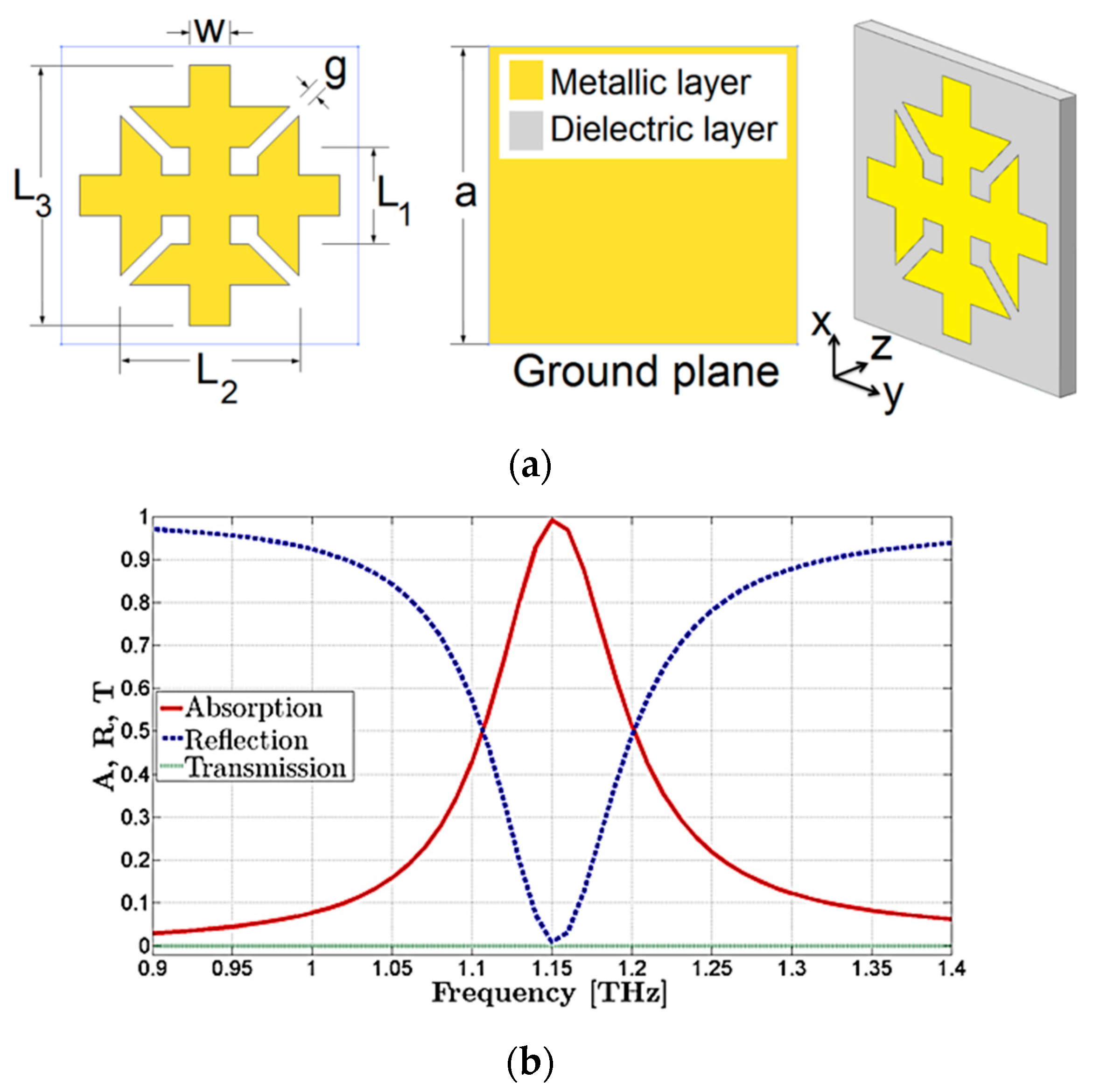
3.1. Narrow Band Absorber

Before the development of the metamaterial absorber, the traditional absorber needed to spot a resistance plate with a thickness of at least one-quarter wavelength in front of the metal plate to defeat the restriction of the traditional absorber working at one-quarter wavelength. This resistor plate becomes very thick and heavy in the long wavelength frequency range (such as microwave frequency), which means that it does not meet the requirements of light and miniaturized devices. In 2008, Landy et al. designed the first metamaterial absorber, successfully overcoming the above difficulties. Within a single unit of the absorber, the electrical coupling is provided by an electric ring resonator (ERR) [14]. The element consists of two standard split ring resonators connected by an induction ring parallel to the split line, as shown in Figure 3. Through the impedance matching principle, the perfect narrowband absorption is realized in the microwave band. The absorber is favored by the industry due to its light structure and high absorption rate.
According to Maxwell’s equations, the adjustment of the resonance frequency can be realized by scaling the size of the metamaterial structure. In the same year, Tao et al. designed the first THz metamaterial absorber with an absorption rate of 70%. After continuous optimization and improvement, Tao et al. designed a kind of MPA composed of an ERR and split wires [39]. Its structure is similar to that designed by Landy et al., as shown in Figure 4, and it is a typical MDM structure of MPA today. In addition, the absorption can be up to 97% for the incident wave at 1.6 THz.
In 2010, Ye et al. proposed an absorber with a composite structure of metallic crosses, which is a near omnidirectional terahertz absorber with high absorption for transverse electric wave (TE) and transverse magnetic wave (TM) [40]. By exciting the magnetic pole in the metal–dielectric layer, the incident light is perfectly absorbed in the thin layer structure, which is about 25 times smaller than the resonance wavelength. Next, Ye et al. designed the absorber with an overlapping structure on this basis to achieve broadband absorption, which is mentioned in Section 3.3 of this paper.
At first, most MPA can only perfectly absorb a certain polarized electromagnetic wave, which means it is very sensitive to the polarization angle of the incident light. This leads to its limited application in many fields, such as solar cells and biosensors. Therefore, polarization-insensitive MPA has become the development requirement for MPA in some fields [41]. In 2017, Astorino et al. designed a polarization-insensitive ultra-thin narrowband absorber [42], which is composed of a top metallic ERR and a bottom ground plane, both made of lossy gold, separated by a thick dielectric layer of benzocyclobutane, as shown in Figure 5. Its absorption structure has four rotational symmetries. It can be found that the high symmetry of the absorber structure can help realize polarization insensitivity.
In recent years, with the development of MPA in the sensing field, the requirements for sensor multi-scene applications are gradually increasing. Flexible materials are widely used in sensing fields, such as biological detection, pressure sensing, flexible artificial skin, etc., due to their excellent characteristics, such as flexibility, low dielectric constant, stable performance, and easy integration into wearable devices.
In 2020, Cheng et al. proposed a planar array Fano asymmetric split ring resonator fabricated on flexible Polyimide (PI) substrate [43] for protein sensing. Its sensitivity was 240 GHz/RIU, which provided the idea for the combination of flexible materials and MPA. In 2021, Wang et al. improved the structure. As shown in Figure 6 [44], the unit structure of the absorber is gold, dielectric (polyimide), and gold, from top to bottom. The upper surface comprises two identical split rings, which are rotated and spliced 180 degrees to form an asymmetric split ring resonator. When there is no substance to be measured, the highest absorption peak is 4.83 THz. By changing the refractive index of the object to be measured, its sensitivity can reach 1018 GHz/RIU [45].
Although the metamaterial absorber with MDM structure can realize the correspondence of most electromagnetic spectrums with novel performance, it also faces some shortcomings due to the existence of metal structure, such as high ohmic loss, high thermal conductivity, and low melting point [45]. These shortcomings limit its application scope. Therefore, the researchers designed a metamaterial absorber with all-dielectric structure, which put forward a new idea for the regulation of electromagnetic field. An all-dielectric metamaterial absorber made of materials with good temperature stability can effectively avoid Joule heating, and has potential applications in energy collection, imaging, and sensing. In 2017, Liu et al. presented a terahertz all-dielectric metasurface absorber based on hybrid dielectric waveguide resonances [46]. By adjusting the geometric structure, the resonance of the electric and magnetic dipole overlapped, thus achieving perfect absorption, as shown in Figure 7. The results show that the absorbance is 97.5% at 1.011 THz. Compared with metal-based methods, all-dielectric absorbers can use near-infrared materials with high melting points and low loss, so they will be used in imaging, thermophotovoltaic, and other sensing applications.
In the same year, Fan et al. realized a metasurface consisting of sub-wavelength cylindrical resonators that achieve diffraction-limited imaging at THz frequencies without cooling [45]. The ingenuity of this design lies in the use of conversion imaging method. As shown in Figure 8, the unit structure is cylindrical dielectric particles, and the medium used here is silicon. As a universal converter of radiation, the all-dielectric metasurface absorber absorbs incident terahertz waves, converts them into heat, and then is detected by infrared cameras. The results show that at the frequency of 603 GHz, the absorbance of all-dielectric metasurface is as high as 96%, and the thermal response rate is as high as 2.16 × 10⁴ K/W. This result can be extended to other spectra, which provides a new way of measuring thermal imaging.

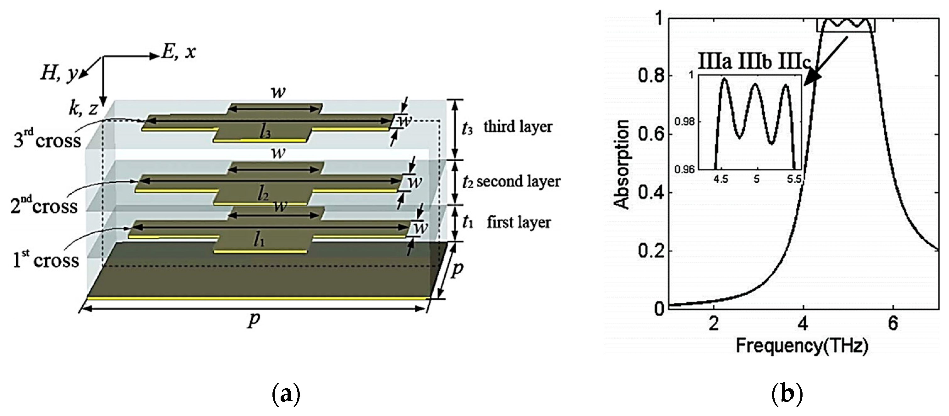
3.2. Dual-Frequency and Multi-Frequency Absorbers

In the design of the MPA structure, usually, there are two ways to achieve dual-frequency absorption, multi-frequency absorption, and even broadband absorption. In the first method, sub-lattice units with various sizes and structures are assembled in one lattice unit, so that different resonance effects occur in each sub-lattice unit or among sub-lattice units. In the second method, MPA is designed as a multi-layer superposition structure, and the structure and size of resonators in each layer are different. The principle is similar to that of the first method. When different resonance absorption peaks are far away, we can get dual-frequency or multi-frequency MPA; when the distance between different resonance peaks is close, or the average absorption between resonance peaks is high, we can get broadband MPA.
In 2009, Wen et al. designed a dual-frequency THz metamaterial absorber. Its ERR unit consists of two symmetrical single resonant metamaterials, one embedded in the other [47]. The results show that MPA has two obvious strong absorption peaks near 0.45 THz and 0.92 THz, both of which are related to the LC resonance of metamaterials, as shown in Figure 9. Compared with single-frequency absorbers, such a design has a wider application range and a broader development prospect. In 2011, Ma et al. also designed a terahertz dual-band metamaterial absorber with metal nested square ring arrays [48]. Its structure is simpler than the former. Two obvious absorption peaks are found at 2.7 THz and 5.2 THz, which are in good agreement with the simulation results, as shown in Figure 10. In addition, the design is highly symmetrical, so it is insensitive to polarization.
In 2015, Shan et al. proposed an ultra-thin flexible dual-band terahertz wave absorber based on metamaterials [49]. The metamaterial structure has two periodic split ring resonators with asymmetric gaps. The results show that the absorber has two resonance absorption peaks at 0.41 THz and 0.75 THz, respectively, and the absorption rates are 92.2% and 97.4%, respectively, as shown in Figure 11. Because the structure is symmetrical, the absorber also has polarization insensitivity. The middle dielectric layer of the absorber is made of polyimide, a flexible material with a thickness of 25 μm, which makes the absorber highly flexible and gives it a non-planar application potential, for instance, for microbolometers and stealth aircraft.
In 2022, Yun et al. designed a dual narrow-band perfect metamaterial absorber suitable for the optical communication band [50], as shown in Figure 12, in which the silicon nanodisc array was placed on a thin gold film separated by a dielectric layer. The results showed that perfect absorption peaks appeared at 1310 nm and 1550 nm, respectively. The absorber had a wide application prospect in the fields of optical communication, frequency-selective optical detection, and inter-satellite laser communication.
In 2019, Wang et al. designed two all-dielectric terahertz plasmonic metamaterial absorbers (PMA) [51]. The cell structures of both PMAs are composed of square arrays of all-dielectric rings and cylindrical disks, and the same heavily doped silicon is used. However, their geometric parameters are different. As shown in Figure 13a, the gap between the two rings is narrow. At this time, PMA can achieve dual-frequency absorption, and there are two different absorption peaks at 0.96 THz and 1.92 THz, with absorption rates of 99.7% and 99.9%, respectively. By changing the inner radius of the ring and the radius of the cylinder, multiple resonance modes can be overlapped, and the Q value can be reduced, so that broadband operation can be obtained, as shown in Figure 13b. Because the quality factor Q of dual-band resonance is larger than that of broadband resonance, it has better sensing performance.
With the development of MPA, perfect multi-band absorption has become a reality. In 2012, Shen et al. designed a terahertz three-band MPA consisting of a square metal piece and two concentric metal square rings with different sizes, as shown in Figure 14 [52]. The results show that there are three different absorption peaks at 0.5 THz, 1.03 THz, and 1.71 THz, and the absorption rates are 96.4%, 96.3%, and 96.7%, respectively. It is simple in structure, easy to fabricate, insensitive to polarization, and has high absorption. In 2016, Wang et al. designed a five-band MPA. The resonant structure of the absorber is two split rings [53], as shown in Figure 15. The working mechanism of five-band near-perfect absorption is due to the joint action of LC, dipole, and surface resonance. The device can be used in the fields of biosensing, material detection, and thermal imaging.

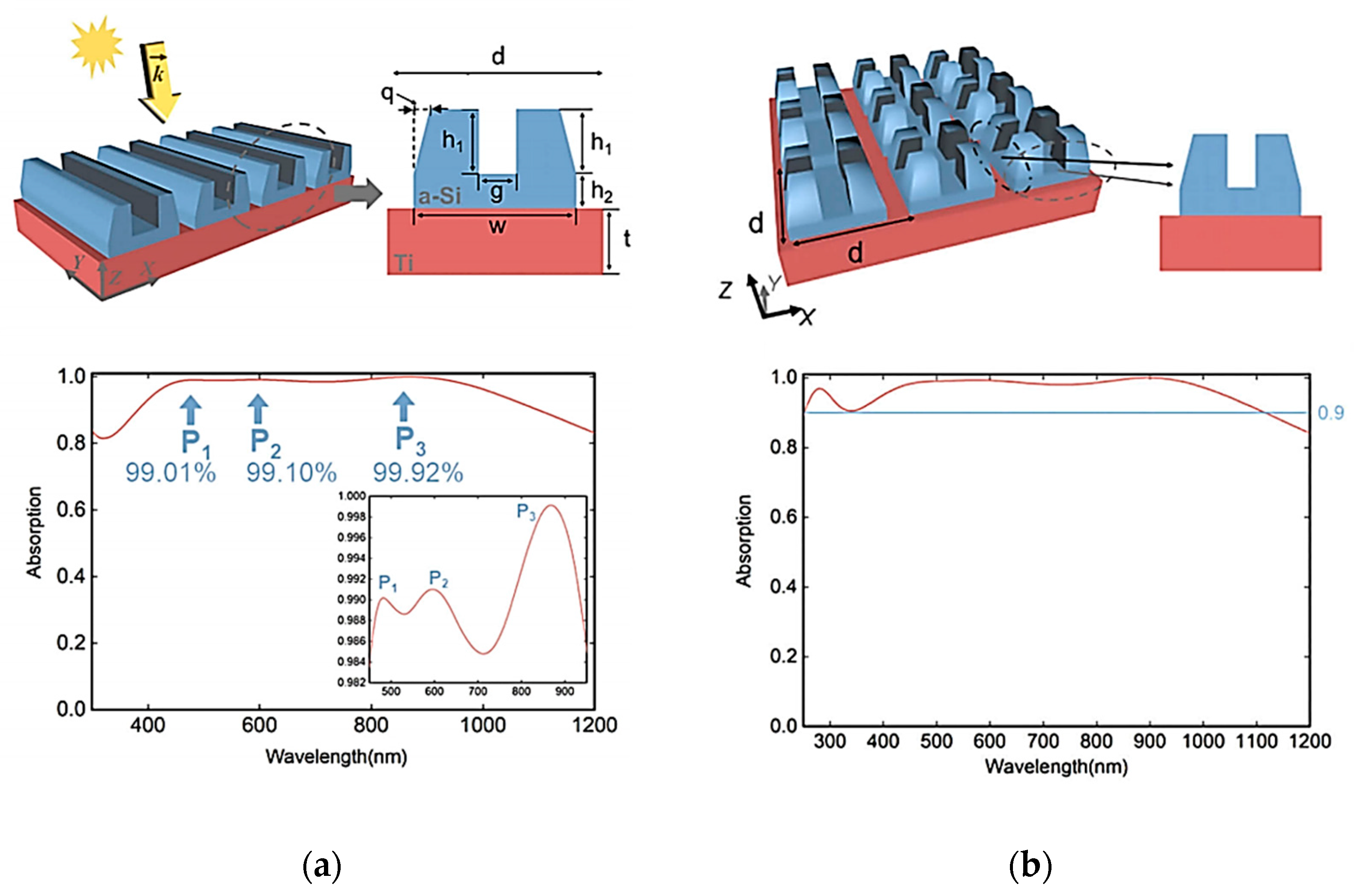
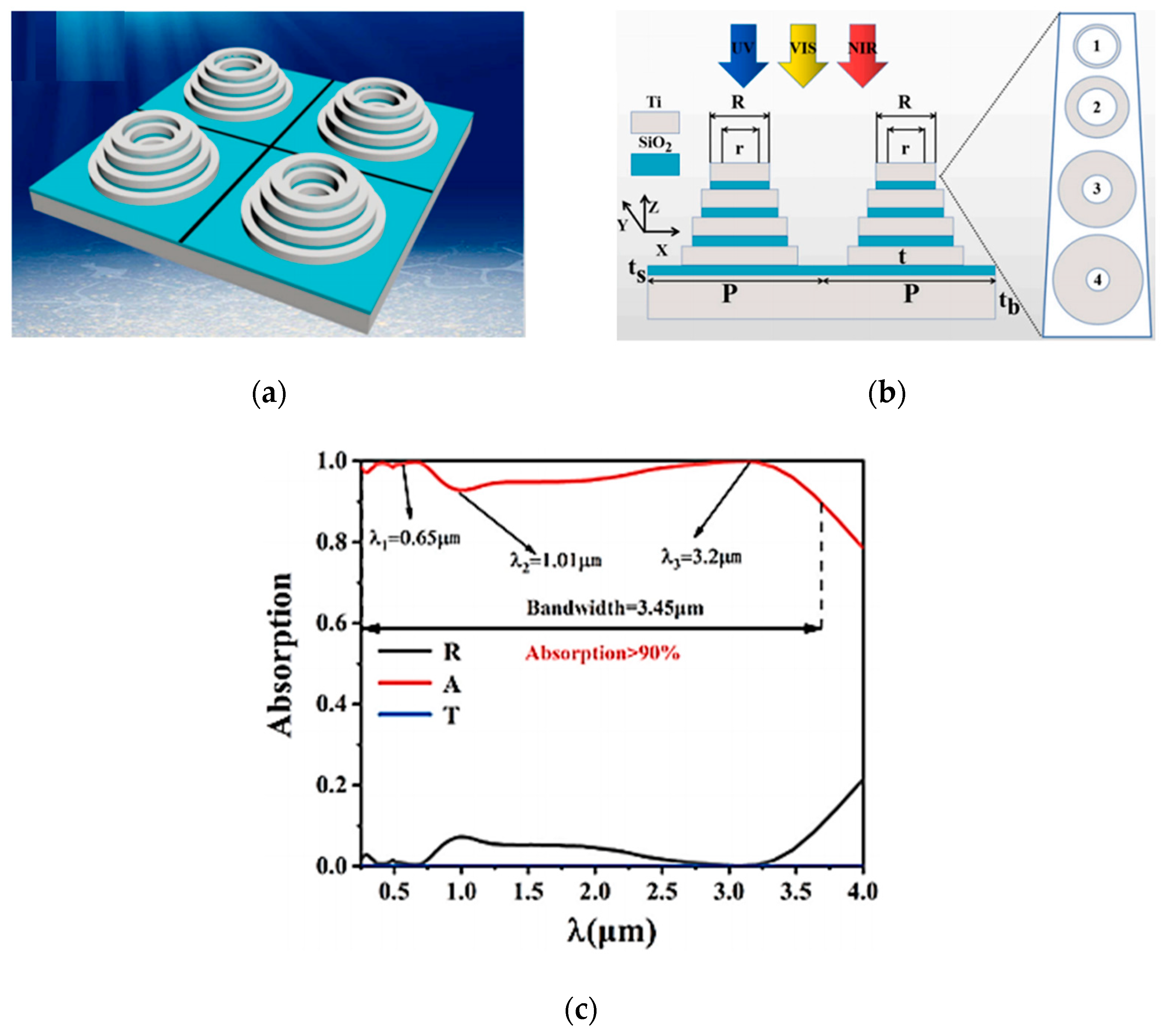
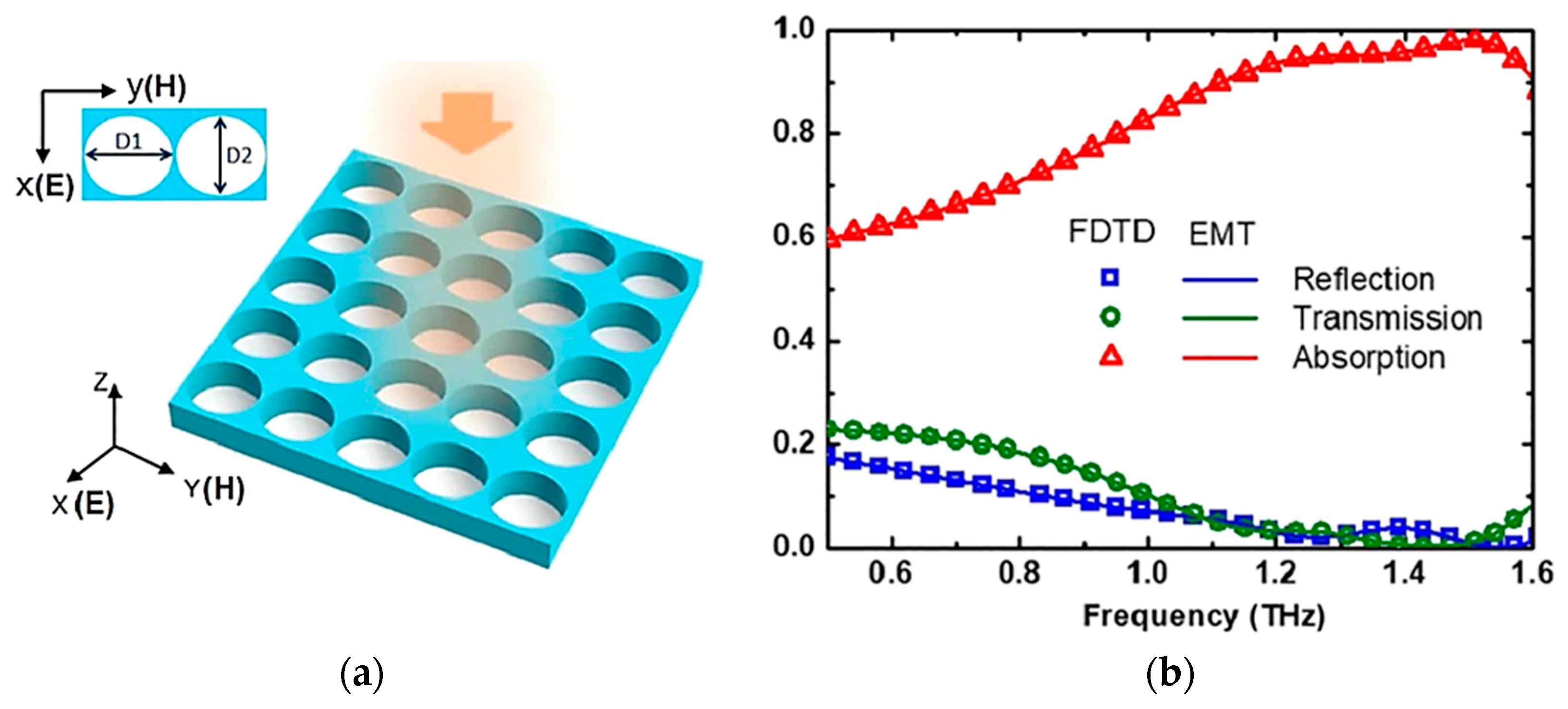
3.3. Broadband Absorber

In many practical applications, such as solar energy collection and photoelectric detectors, researchers hope to obtain absorbers with high average absorption. However, the absorption peaks of multi-frequency absorbers are often discrete, and the average absorption is not high enough. Thus, the perfect absorber with continuous broadband has become the inevitable goal and an important focus for development.
As mentioned above, one of the methods to realize broadband absorption is by assembling sub-lattice units with various sizes in one lattice unit. In 2012, Huang et al. designed a terahertz broadband absorber with three different sizes of “I”-shaped metal structures [54]. As shown in Figure 16, the realization of broadband absorption depends on the superposition of two similar formats. The highest absorbance measured at 0.905 and 0.956 THz is 99.9%, and the minimum absorbance between these two frequencies is still as high as 93%. The absorber can absorb TE or TM polarized terahertz radiation according to the incident direction.
In 2021, Yun et al. designed an ultra-wideband absorber based on multiple resonances [55]. The absorber is composed of amorphous silicon and metallic titanium, and its whole structure comprises grating, as shown in Figure 17. When the visible light is incident in the X polarization direction, the ultra-wideband absorption is realized in the wavelength range of 382 nm to 1100 nm, and three near-perfect absorption bands are obtained. To realize the polarization insensitivity of the absorber and keep excellent absorption performance, Yun et al. improved the above structure to make the unit periodic structure centrosymmetric. The modified absorber can achieve absorption in the range of 0~90° polarization angle.
As mentioned in the previous section, to realize broadband absorption, the absorber is designed as a multi-layer superposition structure and the structure and size of resonators in each layer are different. In 2010, Ye et al. proposed an absorber that could expand the absorption bandwidth by simply stacking several structural layers with different geometric sizes [40], as shown in Figure 18. Three close resonances are observed at 4.55 THz, 4.96 THz, and 5.37 THz. The bandwidth of this strong absorption can be effectively enhanced due to the hybridization of magnetic polarization elements in different layers.
In 2022, Li et al. designed an ultra-wideband absorber with stacked round hole discs [56], as shown in Figure 19. Ultra-wideband absorption can be realized in the whole spectrum (0.25 μm–4 μm). Due to the plasma resonance, the absorber’s absorption rate is more than 90% in the ultra-wide spectral range of 3450 nm, the average absorption rate is 97.5%, and the average absorption rate in the visible light range is more than 99%. Therefore, the absorber shows good performance in the field of solar energy collection and conversion.
In addition to the broadband absorber based on metal structure, the designed all-dielectric metasurface absorber can also achieve broadband absorption. In 2022, Huang et al. introduced a thin-film silicon metasurface absorber with periodic elliptical holes [57], as shown in Figure 20. The absorption performance theory of the absorber is consistent with the experimental results. The absorption of ≥90% starts at 1.1 THz and keeps close to unity until 1.6 THz under normal incidence, and the corresponding bandwidth is 500 GHz. The absorber provides a new idea for modulators, switches, and detectors in the terahertz band.

3.4. Tunable Absorber

Many metamaterial absorbers have been widely studied. However, there are typical defects in the working wavelength and absorption efficiency of metamaterial absorbers, which are determined by the original structure. Once the absorber structure is determined, the optical response will be fixed, and it is difficult to tune flexibly. This defect seriously limits its application as an optical switch or modulator. Therefore, by flexibly adding photosensitive materials, temperature-sensitive materials, liquid crystal materials, or phase-change materials, the absorber can be tuned, effectively broadening the application field. Several tunable absorbers based on different materials will be introduced below.

3.4.1. Tunable Absorber Based on Photosensitive Silicon

A photosensitive semiconductor has an excellent photoelectric conversion effect. When the energy of the pump light source increases, the carrier density in the photosensitive semiconductor will increase synchronously, thus optical control can be realized. Photosensitive silicon is a typical representative. In 2015, Xu et al. showed a metamaterial absorber that can be tuned at terahertz frequency by integrating photosensitive silicon into a metamaterial unit [58], as shown in Figure 21. By changing the pump beam, the conductivity of silicon changes, and thus its optical response can be modified.
In 2019, Zhao et al. demonstrated tunable ultra-wideband terahertz wave absorption by using a single-layer H-type all-silicon array [59], as shown in Figure 22. The absorption is optically tunable. When the pump flux increases from 0 to 4000 J/cm2, the absorption frequency shifts, which in turn changes the absorption width and intensity. The dynamic response of light excitation depends on the penetration depth of pump light in silicon.
In 2020, Wang et al. proposed a single narrow-band THz absorber based on cylindrically shaped periodical p-type doped silicon [60], as shown in Figure 23. The absorber is made of a square polyimide substrate and a cylindrical P-doped silicon array. At 0.57 THz, the absorption rate is close to 99.75%, and the absorption characteristics are good. In addition, by changing the pump luminous flux from 0 to 3000 μJ/cm2, its absorption rate can be flexibly adjusted from above 99% to below 35%. The above two designs provide new ideas for dynamic functional terahertz devices.

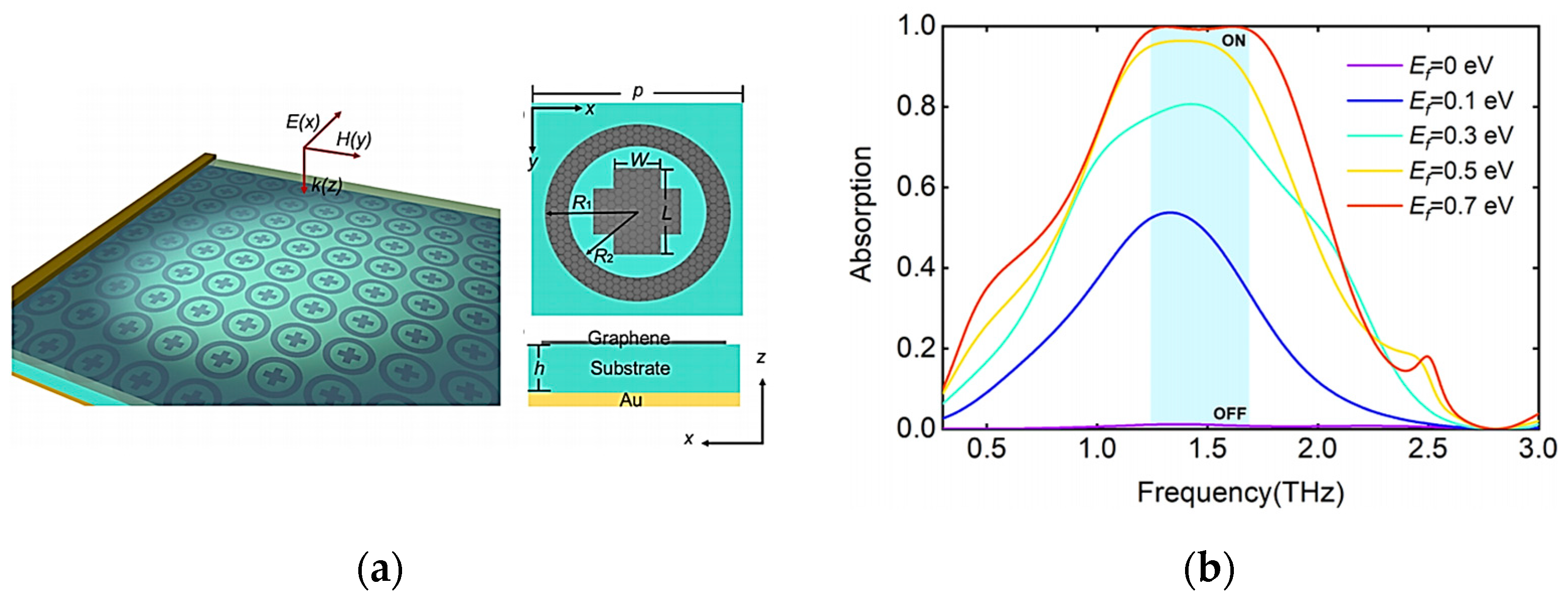
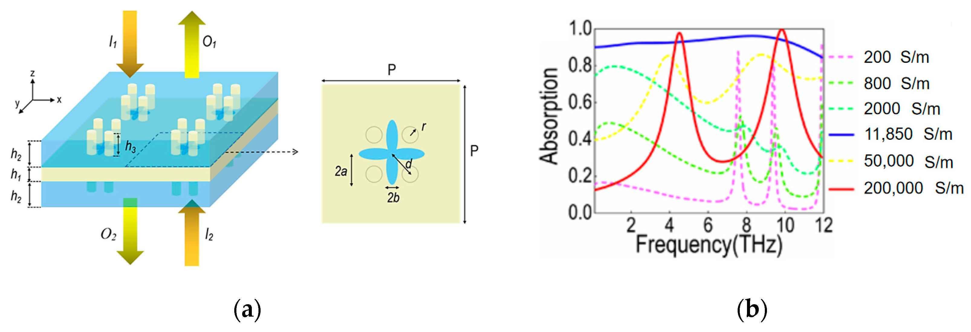
3.4.2. Tunable Absorber Based on Graphene

Graphene is a two-dimensional material. The conductivity of graphene can be controlled by changing the Fermi energy level (EF). EF can be adjusted in a certain range by chemical doping or electrostatic gating [61].
In 2018, Yun et al. demonstrated a dual-band independent tunable absorber composed of stacked graphene nanodiscs, graphene layers with nanohole structure, and metal reflective layers separated by insulator layers [62]. The two absorption peaks A and B in the spectrum are respectively contributed by graphene nanodiscs and graphene layers with nanoholes. The resonance wavelengths corresponding to the two absorption peaks are λA = 11.92 μm and λB = 14.55 μm. Moreover, the TE and TM polarization keep the absorption above 90% in a wide range of incident angles, so the proposed structure is a wide-angle polarization-independent absorber. By changing the Fermi level of graphene nanodiscs and graphene layers with nanoholes, the two absorption peaks of the structure can be tuned independently, as shown in Figure 24. Because of the corresponding wave band and absorption characteristics of the absorber, it can be used in applications related to chemical sensors, detectors, and multi-band infrared absorbers.
In 2019, Yun et al. designed a tunable infrared tri-band perfect absorber based on bilayer graphene, which can adjust the absorption peak by changing the Fermi energy level or the geometrical parameters of the graphene layer [63]. It can be seen from Figure 25 that the intermediate absorption peak depends on the upper graphene layer. With the increase in EF in the upper graphene, the intermediate absorption peak experiences a blue shift. Meanwhile, the left and right absorption peaks depend on the lower layer of L-graphene. When the EF of the lower graphene increases, both the long-wave and short-wave absorption peaks shift blue. This means that there is no coupling effect between the upper and lower layers of graphene during the change of EF. Therefore, the absorber can independently tune the absorption spectrum in a wide spectral range. The absorber can be used in the field of photoelectric detectors, thermal emitters, and photovoltaics.
In 2021, Yun et al. proposed a polarization-insensitive broadband metamaterial absorber based on local surface plasma (LSP) and propagating surface plasma (PSP) [64], as shown in Figure 26. The proposed absorber is designed by the combination of a gold mirror, dielectric layer, and graphene nanostructures. Under the normal irradiation of polarized wave, the absorber has a high absorption, which can be up to 99% from 1.23 to 1.68 THz. The absorption can be nearly tuned from 1% to 99% by adjusting the EF of the graphene. Given the high modulation depth of the absorber, it can be used in thermal emission devices, photovoltaic devices, intelligent absorbers, and active optical switches.

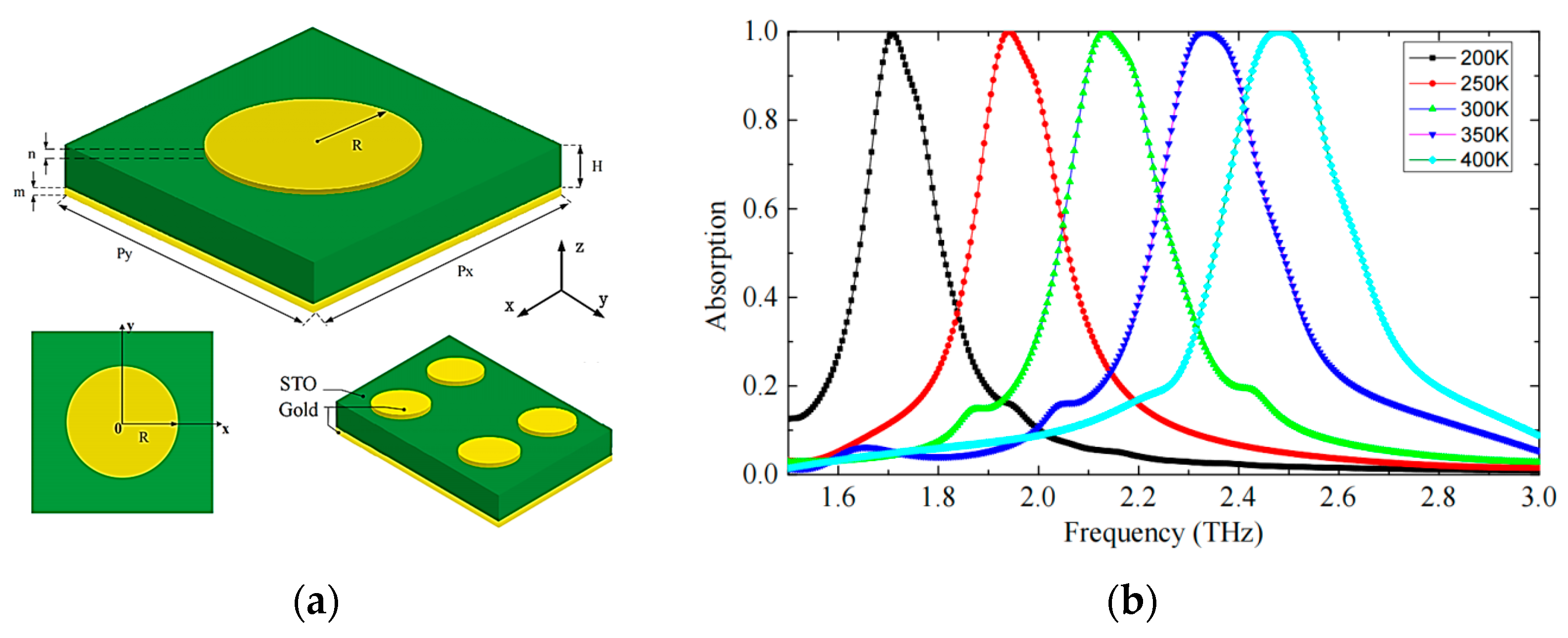
3.4.3. Tunable Absorber Based on Other Materials

At present, phase change materials are also used in the field of tunable absorbers. When the external environment changes, the phase change material can change from one phase to another. VO2 is a typical phase change material that changes with temperature, and the change is reversible. With 341 K as the phase transition point, VO2 changes from the insulation state to the semiconductor state and then to the metal state when the ambient temperature rises gradually. In 2022, Yun et al. proposed a tunable CPA based on VO2 metamaterial in the terahertz frequency range [65], as shown in Figure 27. The CPA realizes intelligent reconfigurable switching modulation from ultra-wideband absorption mode to dual-band absorption mode through VO2 thermal control. When the absorber temperature is controlled at T = 328 K, the conductivity of VO2 can reach 11,850 S/m and then realize the ultra-wideband absorber mode. In this mode, CPA shows an absorption efficiency of more than 90% in the ultra-wideband from 0.1 THz to 10.8 THz. When the conductivity of VO2 reaches 2 × 10⁵ S/m (T = 340 K), CPA switches to dual frequency absorption mode. As described in Section 2.2, the absorption of CPA can be controlled by the phase difference of the incident light. By modulating the phase of the incident light, the absorber can adjust the absorption efficiency to achieve intelligent control from full absorption to high transmittance transmission. In a word, this achievement ingeniously combines a variety of control modes, which can be used to enhance stealth equipment, all-optical switches, and coherent photodetectors.
In addition to VO2, the active material strontium titanate (STO) can also be temperature-regulated, to realize the frequency tunable characteristic. In 2019, Huang et al. designed a thermally tunable metamaterial absorber based on THz strontium titanate [66], as shown in Figure 28. The elliptical pattern on the top of the absorber and the reflective layer are both made of gold material, and the dielectric layer is filled with STO active material. When the temperature dropped from 400 K to 200 K, the center frequency showed a uniform redshift, the tuning range reached 0.77 THz, and the peak absorption remained above 99%. In addition, the absorption bandwidth remains stable, only partially reduced. The structure is simple and ultra-thin, which makes manufacturing easy. In addition, the structure can be extended to other frequencies and has application prospects in imaging, detection, and tunable sensors.
Liquid crystal is a material with variable properties. The voltage-dependent birefringence of nematic liquid crystals has been developed and utilized. By combining liquid crystal with metamaterial, an electronically tunable metamaterial absorber at terahertz frequency can be realized. It provides a new idea for the development of a tunable metamaterial absorber. In 2013, Shrekenhamer and others proposed a liquid crystal tunable metamaterial absorber [67]. The absorber is MDM structure, and the liquid crystal 4′-n-pentyl-4-cyanodiphenyl (5CB) is deposited on the metamaterial array, as shown in Figure 29. When a potential is applied between ERR and the ground plane, LC will be oriented along the electric field line. By changing the applied bias voltage, the absorber achieves 30% amplitude tuning absorption.
In 2021, Zhang et al. proposed a tunable transparent metamaterial absorber with high optical transparency and broadband microwave absorption performance [68]. The absorber consists of three layers. The resonant layer and the reflective layer are made of indium tin oxide (ITO) films, and the dielectric layer is made of distilled water combined with polymethyl methacrylate, as shown in Figure 30. The absorber can achieve ultra-wideband absorption in 5.8~16.2 GHz, and the absorption rate is greater than 90%. The absorption bandwidth and absorption intensity of the absorber can be adjusted by changing the thickness of the water substrate. Increasing the thickness of the water substrate can improve the absorption capacity of high frequency waves and increase the absorption bandwidth. This achievement can be applied to aviation, medical treatment, research facilities and other fields. However, the structure of the absorber is complex, and the requirements for the manufacturing process are high.

4. Conclusions

As MPA develops, it also faces higher development requirements, such as simpler structure, richer functions, and more accurate tuning. In conclusion, metamaterials can overcome the defects of traditional materials. The MPA can be designed in a personalized fashion, and its structure is smaller and lighter, so it is convenient to realize more novel electromagnetic functions, and it has broad application prospects in the field of absorbing materials. It can be seen from this paper that compared with traditional absorbers, MPAs can meet the absorption requirements from narrowband to broadband. Combined with photosensitive silicon, graphene, VO2, and other phase change materials, it can realize optical control, electrical control, and temperature control, and is widely used in sensing, optical switch, communication, stealth equipment, photoelectric detection, and other fields. In theory, MPA can meet the development requirements of miniaturization and integration. However, one of the implementation methods of MPAs is to stack several resonant layers, and its production process inevitably involves multi-layer thin film deposition, which is too complex, so MPAs still face technical challenges in the practical integration of metasurface devices.
In the future, with the maturity of science and technology, MPA will also develop rapidly, and the relevant theory and manufacturing process will also continue to progress. It is expected that MPA will have better performance and be widely used.

Author Contributions

Conceptualization, X.L.; methodology, F.X.; software, X.L.; validation, F.X.; formal analysis, M.W.; resources, J.L.; data curation, X.L.; writing—original draft preparation, X.L.; writing—review and editing, M.Y.; visualization, X.L.; supervision, M.Y. All authors have read and agreed to the published version of the manuscript.

Funding

This research received no external funding.

Institutional Review Board Statement

Not applicable.

Informed Consent Statement

Not applicable.

Data Availability Statement

Data sharing not applicable.

Conflicts of Interest

The authors declare no conflict of interest.

References

  1. Pendry, J.B.; Holden, A.J.; Stewart, W.J.; Youngs, I. Extremely Low Frequency Plasmons in Metallic Mesostructures. Phys. Rev. Lett. 1996, 76, 4773–4776. [Google Scholar] [CrossRef] [PubMed]
  2. Kildishev, A.V.; Boltasseva, A.; Shalaev, V.M. Planar Photonics with Metasurfaces. Science 2013, 339, 6. [Google Scholar] [CrossRef] [PubMed]
  3. He, J.W.; Dong, T.; Chi, B.H.; Zhang, Y. Metasurfaces for Terahertz Wavefront Modulation: A Review. J. Infrared Millim. Terahertz Waves 2020, 41, 607–631. [Google Scholar] [CrossRef]
  4. Veselago, V.G. The Electrodynamics of Substance with Simultaneously Negative Values of E and M. Physics-Uspekhi 1968, 10, 509. [Google Scholar] [CrossRef]
  5. Wei, Z.; Xiaopeng, Z. Advances in Research on Left-Handed Metamaterials. Mater. Rev. 2006, 20, 26. [Google Scholar]
  6. Liu, C.Q.; Zhang, S.; Wang, S.J.; Cai, Q.N.; Wang, P.; Tian, C.S.; Zhou, L.; Wu, Y.Z.; Tao, Z.S. Active Spintronic-Metasurface Terahertz Emitters with Tunable Chirality. Adv. Photonics 2021, 3, 19. [Google Scholar] [CrossRef]
  7. Li, X.J.; Yin, J.; Liu, J.J.; Shu, F.Z.; Lang, T.T.; Jing, X.F.; Hong, Z. Resonant Transparency of a Planar Anapole Metamaterial at Terahertz Frequencies. Photonics Res. 2021, 9, 125–130. [Google Scholar] [CrossRef]
  8. Silalahi, H.M.; Chen, Y.P.; Shih, Y.H.; Chen, Y.S.; Lin, X.Y.; Liu, J.H.; Huang, C.Y. Floating Terahertz Metamaterials with Extremely Large Refractive Index Sensitivities. Photonics Res. 2021, 9, 1970–1978. [Google Scholar] [CrossRef]
  9. Pendry, J.B.; Schurig, D.; Smith, D.R. Controlling Electromagnetic Fields. Science 2006, 312, 1780–1782. [Google Scholar] [CrossRef] [PubMed]
  10. Gao, E.D.; Liu, Z.M.; Li, H.J.; Xu, H.; Zhang, Z.B.; Lu, X.; Xiong, C.X.; Liu, C.; Zhang, B.H.; Zhou, F.Q. Dynamically Tunable Dual Plasmon-Induced Transparency and Absorption Based on a Single-Layer Patterned Graphene Metamaterial. Opt. Express 2019, 27, 13884–13894. [Google Scholar] [CrossRef]
  11. Yu, N.F.; Genevet, P.; Kats, M.A.; Aieta, F.; Tetienne, J.P.; Capasso, F.; Gaburro, Z. Light Propagation with Phase Discontinuities: Generalized Laws of Reflection and Refraction. Science 2011, 334, 333–337. [Google Scholar] [CrossRef] [Green Version]
  12. Pfeiffer, C.; Grbic, A. Metamaterial Huygens’ Surfaces: Tailoring Wave Fronts with Reflectionless Sheets. Phys. Rev. Lett. 2013, 110, 197401. [Google Scholar] [CrossRef] [PubMed]
  13. Liu, N.; Mesch, M.; Weiss, T.; Hentschel, M.; Giessen, H. Infrared Perfect Absorber and Its Application as Plasmonic Sensor. Nano Lett. 2010, 10, 2342–2348. [Google Scholar] [CrossRef]
  14. Landy, N.I.; Sajuyigbe, S.; Mock, J.J.; Smith, D.R.; Padilla, W.J. Perfect Metamaterial Absorber. Phys. Rev. Lett. 2008, 100, 4. [Google Scholar] [CrossRef] [PubMed]
  15. Xu, J.; Li, R.Q.; Qin, J.; Wang, S.Y.; Han, T.C. Ultra-Broadband Wide-Angle Linear Polarization Converter Based on H-Shaped Metasurface. Opt. Express 2018, 26, 20913–20919. [Google Scholar] [CrossRef]
  16. Zhao, J.; Wang, J.X.; Qiu, W.B.; Zhao, Z.Y. Investigation of Sensing Characteristic of Graphene Metamaterial Based on Fano Resonance. Laser Optoelectron. Prog. 2021, 58, 6. [Google Scholar]
  17. Bai, L.; Zhang, X.G.; Jiang, W.; Cui, T. Research Progress of Light-Controlled Electromagnetic Metamaterials. J. Radars 2021, 10, 240–258. [Google Scholar]
  18. Shaltout, A.M.; Shalaev, V.M.; Brongersma, M.L. Spatiotemporal Light Control with Active Metasurfaces. Science 2019, 364, 6591. [Google Scholar] [CrossRef] [PubMed]
  19. Abdulkarim, Y.I.; Alkurt, F.O.; Awl, H.N.; Muhammadsharif, F.F.; Bakir, M.; Dalgac, S.; Karaaslan, M.; Luo, H. An Ultrathin and Dual Band Metamaterial Perfect Absorber Based on Znse for the Polarization-Independent in Terahertz Range. Results Phys. 2021, 26, 11. [Google Scholar] [CrossRef]
  20. Le, D.T.; Tong, B.T.; Nguyen, T.K.T.; Cao, T.N.; Nguyen, H.Q.; Tran, M.C.; Truong, C.L.; Bui, X.K.; Vu, D.L.; Nguyen, T.Q.H. Polarization-Insensitive Dual-Band Terahertz Metamaterial Absorber Based on Asymmetric Arrangement of Two Rectangular-Shaped Resonators. Optik 2021, 245, 8. [Google Scholar] [CrossRef]
  21. Lu, T.G.; Zhang, D.W.; Qiu, P.Z.; Lian, J.Q.; Jing, M.; Yu, B.B.; Wen, J. Ultrathin Terahertz Dual-Band Perfect Metamaterial Absorber Using Asymmetric Double-Split Rings Resonator. Symmetry 2018, 10, 293. [Google Scholar] [CrossRef]
  22. Schalch, J.; Duan, G.W.; Zhao, X.G.; Zhang, X.; Averitt, R.D. Terahertz Metamaterial Perfect Absorber with Continuously Tunable Air Spacer Layer. Appl. Phys. Lett. 2018, 113, 5. [Google Scholar] [CrossRef]
  23. Vasic, B.; Gajic, R. Graphene Induced Spectral Tuning of Metamaterial Absorbers at Mid-Infrared Frequencies. Appl. Phys. Lett. 2013, 103, 4. [Google Scholar] [CrossRef]
  24. Ma, W.; Wen, Y.Z.; Yu, X.M. Broadband Metamaterial Absorber at Mid-Infrared Using Multiplexed Cross Resonators. Opt. Express 2013, 21, 30724–30730. [Google Scholar] [CrossRef] [PubMed]
  25. Zhu, W.R.; Zhao, X.P.; Gong, B.Y.; Liu, L.H.; Su, B. Optical Metamaterial Absorber Based on Leaf-Shaped Cells. Appl. Phys. A-Mater. Sci. Process 2011, 102, 147–151. [Google Scholar] [CrossRef]
  26. Zhu, W.R.; Zhao, X.P. Metamaterial Absorber with Dendritic Cells at Infrared Frequencies. J. Opt. Soc. Am. B-Opt. Phys. 2009, 26, 2382–2385. [Google Scholar] [CrossRef]
  27. Li, M.L.; Muneer, B.; Yi, Z.X.; Zhu, Q. A Broadband Compatible Multispectral Metamaterial Absorber for Visible, near-Infrared, and Microwave Bands. Adv. Opt. Mater. 2018, 6, 9. [Google Scholar] [CrossRef]
  28. Teperik, T.V.; de Abajo, F.J.G.; Borisov, A.G.; Abdelsalam, M.; Bartlett, P.N.; Sugawara, Y.; Baumberg, J.J. Omnidirectional Absorption in Nanostructured Metal Surfaces. Nat. Photonics 2008, 2, 299–301. [Google Scholar] [CrossRef]
  29. Feng, R.; Ding, W.Q.; Liu, L.H.; Chen, L.X.; Qiu, J.; Chen, G.Q. Dual-Band Infrared Perfect Absorber Based on Asymmetric T-Shaped Plasmonic Array. Opt. Express 2014, 22, A335–A343. [Google Scholar] [CrossRef]
  30. Lee, H.S.; Lee, E.H. Analysis of Optical Impedance Matching and Polarization Matching for Integration of Surface Plasmon Polariton Waveguides and Dielectric Waveguides. J. Korean Phys. Soc. 2010, 57, 1737–1742. [Google Scholar] [CrossRef]
  31. Hedayati, M.K.; Zillohu, A.U.; Strunskus, T.; Faupel, F.; Elbahri, M. Plasmonic Tunable Metamaterial Absorber as Ultraviolet Protection Film. Appl. Phys. Lett. 2014, 104, 5. [Google Scholar] [CrossRef]
  32. Mattiucci, N.; Bloemer, M.J.; Akozbek, N.; D’Aguanno, G. Impedance Matched Thin Metamaterials Make Metals Absorbing. Sci. Rep. 2013, 3, 11. [Google Scholar] [CrossRef] [PubMed]
  33. Duan, G.W.; Schalch, J.; Zhao, X.G.; Li, A.B.; Chen, C.X.; Averitt, R.D.; Zhang, X. A Survey of Theoretical Models for Terahertz Electromagnetic Metamaterial Absorbers. Sens. Actuator A-Phys. 2019, 287, 21–28. [Google Scholar] [CrossRef]
  34. Ghosh, S.; Srivastava, K.V. An Equivalent Circuit Model of Fss-Based Metamaterial Absorber Using Coupled Line Theory. IEEE Antennas Wirel. Propag. Lett. 2015, 14, 511–514. [Google Scholar] [CrossRef]
  35. Ming, X.S.; Liu, X.Y.; Sun, L.Q.; Padilla, W.J. Degenerate Critical Coupling in All-Dielectric Metasurface Absorbers. Opt. Express 2017, 25, 24658–24669. [Google Scholar] [CrossRef]
  36. Rothenberg, J.M.; Chen, C.P.; Ackert, J.J.; Dadap, J.I.; Knights, A.P.; Bergman, K.; Osgood, R.M.; Grote, R.R. Experimental Demonstration of Coherent Perfect Absorption in a Silicon Photonic Racetrack Resonator. Opt. Lett. 2016, 41, 2537–2540. [Google Scholar] [CrossRef]
  37. Dutta-Gupta, S.; Martin, O.J.F.; Gupta, S.D.; Agarwal, G.S. Controllable Coherent Perfect Absorption in a Composite Film. Opt. Express 2012, 20, 1330–1336. [Google Scholar] [CrossRef]
  38. Luo, X.; Cheng, Z.Q.; Zhai, X.; Liu, Z.M.; Li, S.Q.; Liu, J.P.; Wang, L.L.; Lin, Q.; Zhou, Y.H. A Tunable Dual-Band and Polarization-Insensitive Coherent Perfect Absorber Based on Double-Layers Graphene Hybrid Waveguide. Nanoscale Res. Lett. 2019, 14, 8. [Google Scholar] [CrossRef]
  39. Tao, H.; Landy, N.I.; Bingham, C.M.; Zhang, X.; Averitt, R.D.; Padilla, W.J. A Metamaterial Absorber for the Terahertz Regime: Design, Fabrication and Characterization. Opt. Express 2008, 16, 7181–7188. [Google Scholar] [CrossRef] [PubMed]
  40. Ye, Y.Q.; Jin, Y.; He, S.L. Omnidirectional, Polarization-Insensitive and Broadband Thin Absorber in the Terahertz Regime. J. Opt. Soc. Am. B-Opt. Phys. 2010, 27, 498–504. [Google Scholar] [CrossRef]
  41. Abdulkarim, Y.I.; Awl, H.N.; Alkurt, F.O.; Muhammadsharif, F.F.; Saeed, S.R.; Karaaslan, M.; Bakir, M.; Luo, H. A Thermally Stable and Polarization Insensitive Square-Shaped Water Metamaterial with Ultra-Broadband Absorption. J. Mater. Res. Technol.-JMRT 2021, 13, 1150–1158. [Google Scholar] [CrossRef]
  42. Astorino, M.D.; Frezza, F.; Tedeschi, N. Ultra-Thin Narrow-Band, Complementary Narrow-Band, and Dual-Band Metamaterial Absorbers for Applications in the Thz Regime. J. Appl. Phys. 2017, 121, 10. [Google Scholar] [CrossRef]
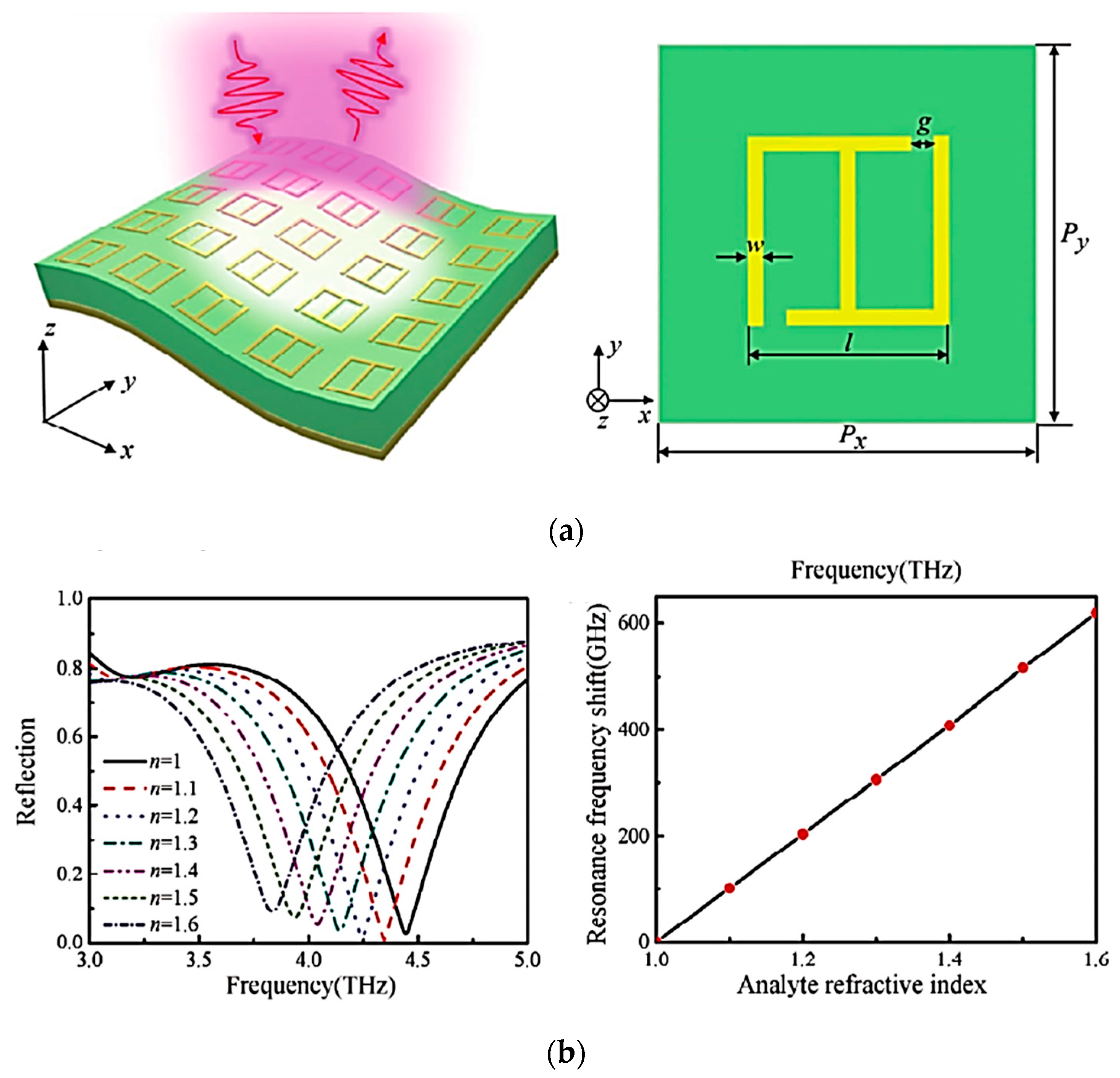
  43. Cheng, R.J.; Xu, L.; Yu, X.; Zou, L.E.; Shen, Y.; Deng, X.H. High-Sensitivity Biosensor for Identification of Protein Based on Terahertz Fano Resonance Metasurfaces. Opt. Commun. 2020, 473, 4. [Google Scholar] [CrossRef]
  44. Wang, S.; Wang, Z.; Cao, T. Design of Terahertz Ultra-High Sensitivity Biosensor Based on Flexible Metamaterial. Electron. Compon. Mater. 2021, 40, 882–887. [Google Scholar]
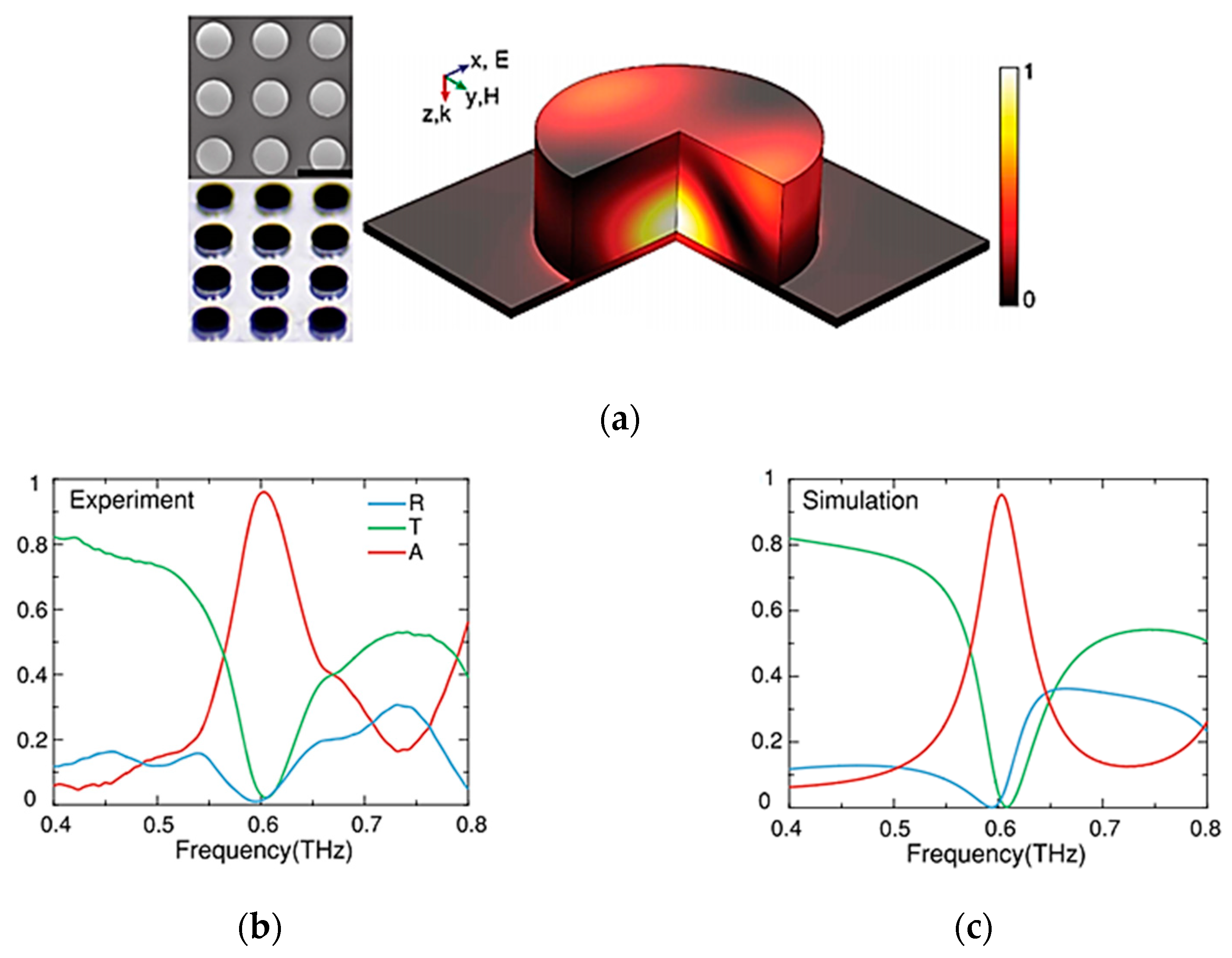
  45. Fan, K.B.; Suen, J.Y.; Liu, X.Y.; Padilla, W.J. All-Dielectric Metasurface Absorbers for Uncooled Terahertz Imaging. Optica 2017, 4, 601–604. [Google Scholar] [CrossRef]
  46. Liu, X.Y.; Fan, K.B.; Shadrivov, I.V.; Padilla, W.J. Experimental Realization of a Terahertz All-Dielectric Metasurface Absorber. Opt. Express 2017, 25, 191–201. [Google Scholar] [CrossRef]
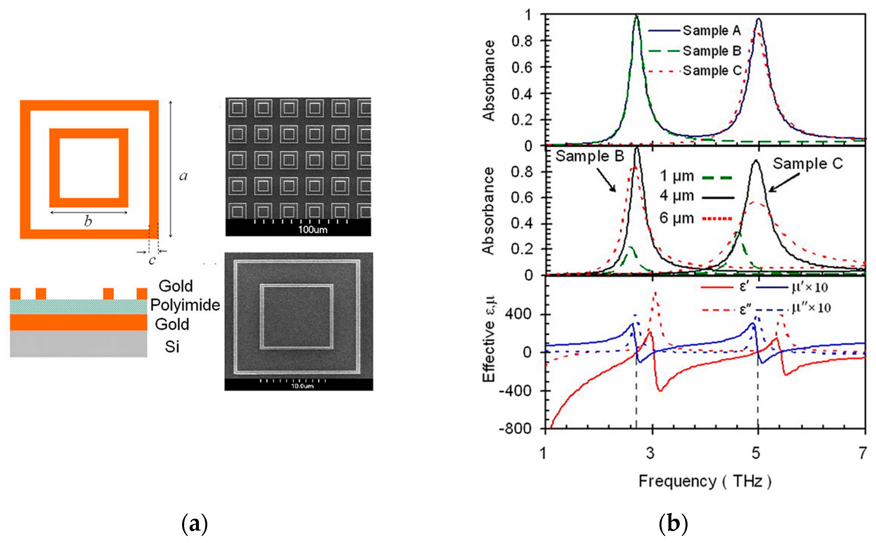
  47. Wen, Q.Y.; Zhang, H.W.; Xie, Y.S.; Yang, Q.H.; Liu, Y.L. Dual Band Terahertz Metamaterial Absorber: Design, Fabrication, and Characterization. Appl. Phys. Lett. 2009, 95, 3. [Google Scholar] [CrossRef]
  48. Ma, Y.; Chen, Q.; Grant, J.; Saha, S.C.; Khalid, A.; Cumming, D.R.S. A Terahertz Polarization Insensitive Dual Band Metamaterial Absorber. Opt. Lett. 2011, 36, 945–947. [Google Scholar] [CrossRef]
  49. Shan, Y.; Chen, L.; Shi, C.; Cheng, Z.X.; Zang, X.F.; Xu, B.Q.; Zhu, Y.M. Ultrathin Flexible Dual Band Terahertz Absorber. Opt. Commun. 2015, 350, 63–70. [Google Scholar] [CrossRef]
  50. Xie, W.L.; Sun, P.; Wang, J.; Feng, H.; Luo, Q.P.; Xie, Q.; Guo, L.H.; Zhang, Z.X.; Sun, J.F.; Zhao, Q.; et al. Polarization-Independent Dual Narrow-Band Perfect Metamaterial Absorber for Optical Communication. Microw. Opt. Technol. Lett. 2022, 64, 1310–1316. [Google Scholar] [CrossRef]
  51. Wang, Y.; Zhu, D.Y.; Cui, Z.J.; Hou, L.; Lin, L.; Qu, F.F.; Liu, X.X.; Nie, P.C. All-Dielectric Terahertz Plasmonic Metamaterial Absorbers and High-Sensitivity Sensing. ACS Omega 2019, 4, 18645–18652. [Google Scholar] [CrossRef]
  52. Shen, X.P.; Yang, Y.; Zang, Y.Z.; Gu, J.Q.; Han, J.G.; Zhang, W.L.; Cui, T.J. Triple-Band Terahertz Metamaterial Absorber: Design, Experiment, and Physical Interpretation. Appl. Phys. Lett. 2012, 101, 4. [Google Scholar] [CrossRef]
  53. Wang, B.X.; Wang, G.Z. Two Compact SRR Resonators Enabling Five-Band Perfect Absorption. Mater. Lett. 2016, 180, 317–321. [Google Scholar] [CrossRef]
  54. Huang, L.; Chowdhury, D.R.; Ramani, S.; Reiten, M.T.; Luo, S.N.; Taylor, A.J.; Chen, H.T. Experimental Demonstration of Terahertz Metamaterial Absorbers with a Broad and Flat High Absorption Band. Opt. Lett. 2012, 37, 154–156. [Google Scholar] [CrossRef] [PubMed] [Green Version]
  55. Feng, H.; Li, X.M.; Wang, M.; Xia, F.; Zhang, K.; Kong, W.J.; Dong, L.F.; Yun, M.J. Ultrabroadband Metamaterial Absorbers from Ultraviolet to near-Infrared Based on Multiple Resonances for Harvesting Solar Energy. Opt. Express 2021, 29, 6000–6010. [Google Scholar] [CrossRef]
  56. Li, X.; Chen, Y.T.; Chen, J.; Jiang, X.P.; He, J.; Jing, Q.; Yang, J.B. Full Spectrum Ultra-Wideband Absorber with Stacked Round Hole Disks. Optik 2022, 249, 9. [Google Scholar] [CrossRef]
  57. Huang, Y.W.; Kaj, K.; Chen, C.X.; Yang, Z.W.; Ul Haque, S.R.; Zhang, Y.; Zhao, X.G.; Averitt, R.D.; Zhang, X. Broadband Terahertz Silicon Membrane Metasurface Absorber. ACS Photonics 2022, 9, 1150–1156. [Google Scholar] [CrossRef]
  58. Xu, Z.C.; Gao, R.M.; Ding, C.F.; Wu, L.; Zhang, Y.T.; Yao, J.Q. Photoexcited Broadband Blueshift Tunable Perfect Terahertz Metamaterial Absorber. Opt. Mater. 2015, 42, 148–151. [Google Scholar] [CrossRef]
  59. Zhao, X.G.; Wang, Y.; Schalch, J.; Duan, G.W.; Crernin, K.; Zhang, J.D.; Chen, C.X.; Averitt, R.D.; Zhang, X. Optically Modulated Ultra-Broadband All-Silicon Metamaterial Terahertz Absorbers. ACS Photonics 2019, 6, 830–837. [Google Scholar] [CrossRef]
  60. Wang, Y.; Yue, L.S.; Cui, Z.J.; Zhang, X.J.; Zhang, X.; Zhu, Y.Q.; Zhang, K. Optically Tunable Single Narrow Band All-Dielectric Terahertz Metamaterials Absorber. AIP Adv. 2020, 10, 7. [Google Scholar] [CrossRef]
  61. Lan, J.X.; Zhang, R.X.; Bai, H.; Zhang, C.D.; Zhang, X.; Hu, W.; Wang, L.; Lu, Y.Q. Tunable Broadband Terahertz Absorber Based on Laser-Induced Graphene. Chin. Opt. Lett. 2022, 20, 4. [Google Scholar] [CrossRef]
  62. Sun, P.; You, C.L.; Mahigir, A.; Liu, T.T.; Xia, F.; Kong, W.J.; Veronis, G.; Dowling, J.P.; Dong, L.F.; Yun, M.J. Graphene-Based Dual-Band Independently Tunable Infrared Absorber. Nanoscale 2018, 10, 15564–15570. [Google Scholar] [CrossRef]
  63. Wu, D.; Wang, M.; Feng, H.; Xu, Z.X.; Liu, Y.P.; Xia, F.; Zhang, K.; Kong, W.J.; Dong, L.F.; Yun, M.J. Independently Tunable Perfect Absorber Based on the Plasmonic Properties in Double-Layer Graphene. Carbon 2019, 155, 618–623. [Google Scholar] [CrossRef]
  64. Feng, H.; Xu, Z.X.; Li, K.; Wang, M.; Xie, W.L.; Luo, Q.P.; Chen, B.Y.; Kong, W.J.; Yun, M.J. Tunable Polarization-Independent and Angle-Insensitive Broadband Terahertz Absorber with Graphene Metamaterials. Opt. Express 2021, 29, 7158–7167. [Google Scholar] [CrossRef]
  65. Zhang, Z.X.; Xie, Q.; Guo, L.H.; Su, C.X.; Wang, M.; Xia, F.; Sun, J.F.; Li, K.; Feng, H.; Yun, M.J. Dual-Controlled Tunable Dual-Band and Ultra-Broadband Coherent Perfect Absorber in the Thz Range. Opt. Express 2022, 30, 30832–30844. [Google Scholar] [CrossRef] [PubMed]
  66. Huang, X.; He, W.; Yang, F.; Ran, J.; Yang, Q.; Xie, S.Y. Thermally Tunable Metamaterial Absorber Based on Strontium Titanate in the Terahertz Regime. Opt. Mater. Express 2019, 9, 1377–1385. [Google Scholar] [CrossRef]
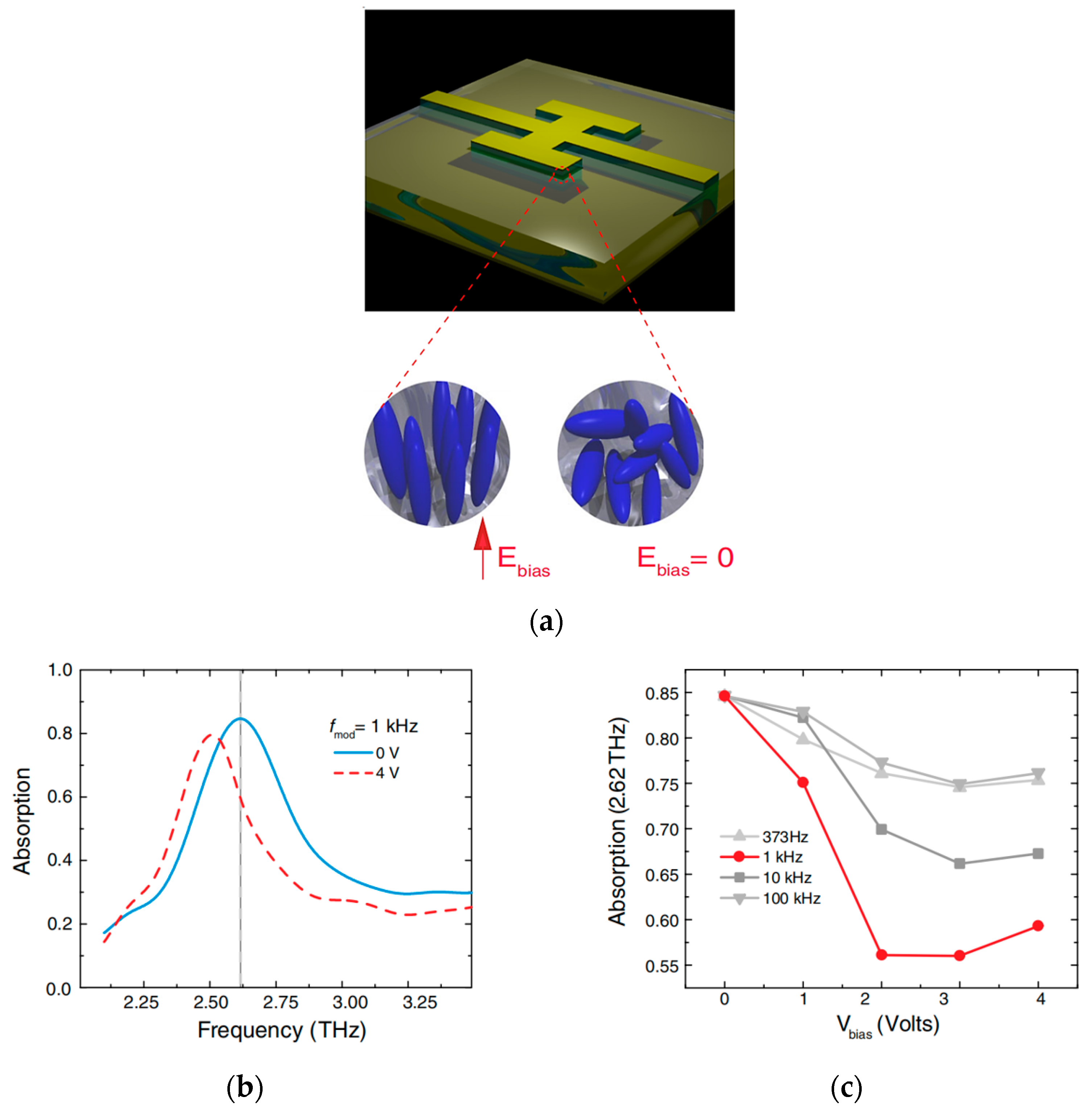
  67. Shrekenhamer, D.; Chen, W.C.; Padilla, W.J. Liquid Crystal Tunable Metamaterial Absorber. Phys. Rev. Lett. 2013, 110, 177403. [Google Scholar] [CrossRef]
  68. Zhang, Y.Q.; Dong, H.X.; Mou, N.L.; Li, H.N.; Yao, X.; Zhang, L. Tunable and Transparent Broadband Metamaterial Absorber with Water-Based Substrate for Optical Window Applications. Nanoscale 2021, 13, 7831–7837. [Google Scholar] [CrossRef]
Figure 1. Schematic diagram of transmission line modelling of metamaterial absorber [33].
Photonics 10 00205 g001
Figure 2. Multi−reflection diagram of the metamaterial layer and base reflection layer [33].
Photonics 10 00205 g002
Figure 3. (a) The structure of the MPA unit was designed by Landy et al. [14]; (b) absorption, reflection, and projection curves [14].
Photonics 10 00205 g003
Figure 4. Schematic diagram of the perfect absorber for terahertz band designed by Tao et al. [39] (a) Electric resonator on the top of a polyimide spacer; (b) cut wire on GaAs wafer; (c) single unit cell showing the direction of propagation of incident EM wave.
Photonics 10 00205 g004
Figure 5. (a) Structure of polarization-insensitive ultra-thin narrowband absorber; (b) absorption, reflection, and transmission curves [42].
Photonics 10 00205 g005
Figure 6. MPA biosensor. (a) Sensor structure; (b) reflection curve with the change of refractive index of the detected object [44].
Photonics 10 00205 g006
Figure 7. Simulated spectral reflectance (blue), transmittance (black), and absorbance (red) [46].
Photonics 10 00205 g007
Figure 8. (a) Scanning electron microscopic image of fabricated cylinder array; (b) measured reflectance R (blue), transmittance T (green), and absorbance A (red) of the dielectric absorber; (c) numerically simulated R, T, and A [45].
Photonics 10 00205 g008
Figure 9. Dual frequency terahertz metamaterial absorber. (a) Top view; (b) the main view; (c) reflection and absorption curves [47].
Photonics 10 00205 g009
Figure 10. (a) Structure and SEM of the terahertz dual−band metamaterial absorber; (b) absorption curves and calculated effective dielectric constant and permeability under different structural parameters [48].
Photonics 10 00205 g010
Figure 11. (a) Structure and (b) absorption curve of the ultra-thin flexible dual-band terahertz absorber [49].
Photonics 10 00205 g011
Figure 12. A dual-narrowband perfect metamaterial absorber suitable for optical communication band [50]. (a) The structure; (b) the curve of absorption.
Photonics 10 00205 g012
Figure 13. (a) SEM image of the designed PMAs; (b) illustrations of unit cells of SRRs and simulated (yellow curve) and measured (green curve) absorption characteristics of the broadband PMAs [51].
Photonics 10 00205 g013
Figure 14. Terahertz tri-band MPA. (a) The structure; (b) the curve of absorption [52].
Photonics 10 00205 g014
Figure 15. Five-band MPA. (a) Structure; (b) absorption curve [53].
Photonics 10 00205 g015
Figure 16. The whole unit cell of the Terahertz broadband absorber [54]. (a) Schematic of the whole unit cell; and (b) top view of the metamaterial absorber with dimensions. (c) Numerical simulation results of absorption spectra at normal incidence for three different configurations of the I-shaped resonators.
Photonics 10 00205 g016
Figure 17. (a) Structure and absorption curve of the ultra-wideband absorber; (b) polarization insensitive structure, and absorption curve after optimization [55].
Photonics 10 00205 g017
Figure 18. (a) Structure of multilayer broadband absorber; (b) the absorption curve [40].
Photonics 10 00205 g018
Figure 19. (a) Full spectrum absorber structure diagram; (b) full spectrum absorber plan; (c) full spectrum absorption spectrum, reflection spectrum, and transmission spectrum [56].
Photonics 10 00205 g019
Figure 20. (a) Schematic of the broadband THz silicon membrane metasurface absorber (SMMA); (b) simulated reflection (blue), transmission (green), and absorption (red) of SMMA [57].
Photonics 10 00205 g020
Figure 21. Tunable metamaterial absorber based on photosensitive silicon (a) structure and (b) absorption curve with silicon conductivity [58].
Photonics 10 00205 g021
Figure 22. (a) Scanning electron microscope image of the all-silicon; (b) OPTP spectrum of the all-dielectric MPA for different pump fluences [59].
Photonics 10 00205 g022
Figure 23. (a) Schematic structure of the sample; (b) the absorption of the proposed absorber for different pump fluences [60].
Photonics 10 00205 g023
Figure 24. Dual-band independent tunable absorber (a) structure, and (b) absorption curves of graphene nanodiscs and graphene layers at different Fermi energy levels [62].
Photonics 10 00205 g024
Figure 25. (a) Structure of graphene-based infrared band absorber and (b) corresponding absorption spectra of graphene nanodisc and L-type single-layer graphene array at different Fermi levels [63].
Photonics 10 00205 g025
Figure 26. (a) The structure of the polarization-insensitive broadband metamaterial absorber based on graphene and (b) the broadband absorption curve with EF [64].
Photonics 10 00205 g026
Figure 27. (a) The structure of a tunable coherent perfect absorber based on VO2 metamaterial and (b) the absorption curve changing with VO2 conductivity [65].
Photonics 10 00205 g027
Figure 28. (a) The proposed tunable terahertz absorber with a classical sandwiched structure consisted of a metallic top layer and ground plane, spaced by STO material film; (b) absorption spectra of the absorber with different temperatures of 200 K, 250 K, 300 K, 350 K, and 400 K under normal incidence [66].
Photonics 10 00205 g028
Figure 29. (a) Rendering of a single unit cell of the liquid crystal metamaterial absorber; (b) frequency dependent absorption for 0 V (blue solid curve) and 4 V (red dashed curve) at fmod = 1 kHz; (c) the absorption value at 2.62 THz as a function of bias voltage (Vbias) for various modulation frequencies [67].
Photonics 10 00205 g029
Figure 30. (a) Schematic diagram of the tunable, transparent metamaterial absorber with a water-based substrate; (b) simulated absorption spectra for normal incident waves with different hwaters from 0 mm to 1.2 mm [68].
Photonics 10 00205 g030
Disclaimer/Publisher’s Note: The statements, opinions and data contained in all publications are solely those of the individual author(s) and contributor(s) and not of MDPI and/or the editor(s). MDPI and/or the editor(s) disclaim responsibility for any injury to people or property resulting from any ideas, methods, instructions or products referred to in the content.

