1. Introduction
Nitride-based light-emitting diodes (LEDs) have gained significant attention due to their potential for high-brightness and energy-efficient lighting applications [
1,
2,
3,
4]. However, in the heteroepitaxial growth of the GaN film, crystal defects, serving as non-radiative recombination centers, are often observed due to the substantial lattice mismatch between the sapphire substrate and the GaN film [
5,
6]. To realize high-brightness and high-reliability LEDs, researchers are continuously working to improve LED efficiency and performance through various techniques such as nonpolar growth, SiN treatment, and surface nanostructure techniques [
7,
8,
9]. The presence of crystal defects, particularly V-defects, can significantly impact the reverse properties, such as reverse leakage current, breakdown voltage and breakdown conductive channel, in GaN-based LEDs, affecting their overall reliability and functionality [
5,
6,
10]. V-defects refer to V-shaped pits or grooves that form during the epitaxial growth of GaN material [
11]. These defects can have both positive and negative effects on the performance of LEDs [
11,
12]. On one hand, V-defects can act as scattering centers, enhancing the light extraction efficiency by redirecting trapped photons [
12]. On the other hand, V-defects can introduce non-uniformities in the well thickness and In content, leading to variations in emission wavelength and reduced overall efficiency [
13,
14]. One of the critical issues associated with V-defects is reverse leakage current [
15,
16]. Crystal defects introduce localized regions with different energy levels, acting as trap sites for charge carriers [
16]. Under reverse bias conditions, charge carriers can tunnel through these trap states, causing reverse tunneling leakage current [
16]. High densities of V-defects can exacerbate this phenomenon, leading to localized hotspots and accelerating the breakdown process [
17]. Consequently, the breakdown voltage of the LED decreases with increasing reverse leakage current.
Furthermore, the presence of crystal defects, including V-defects, can also impact the reverse leakage current and breakdown phenomena in GaN-based LEDs [
16,
17]. V-defects can act as preferential paths for current leakage, diverting carriers away from the intended active region. This can lead to non-radiative recombination, reducing the efficiency of the LED and hindering the proper operation of the device [
18]. In addition, crystal defects can introduce non-radiative recombination centers, generating heat instead of light, further decreasing the LED’s overall efficiency [
19]. To address these challenges, researchers and LED manufacturers focus on various strategies to minimize crystal defects during epitaxial growth [
20,
21,
22]. Advanced epitaxial growth techniques, such as MOCVD and MBE, and substrate engineering methods, like patterned sapphire substrates, are used to reduce the occurrence of V-defects and improve LED performance [
23,
24,
25]. Additionally, improved passivation techniques are employed to protect the LED surface and interfaces, reducing surface-related degradation and enhancing device stability [
26]. In particular, the surface V-defects can have a significant effect on the formation of local breakdown phenomena in GaN-based LEDs, which can create preferential paths for carriers, leading to a localized region with enhanced conductivity [
10,
27,
28]. These paths act as n-type carrier paths, similar to an n-type electrode, and facilitate the flow of electrons during forward and reverse biases, thereby affecting the luminescence and breakdown behaviors. In this study, we investigate the impact of V-defects on the electrical properties of breakdown conductive channels in GaN-based LEDs. The formation of local breakdown conductive channels is systematically studied by varying the size, distribution, and density of surface V-defects within the LED structure.
2. Materials and Methods
GaN-based LEDs were grown on (0001) sapphire substrates using a home-made metal–organic chemical vapor deposition system. The epitaxial growth process involved the deposition of various layers, including 2.0 μm thick undoped GaN, 3.0 μm thick n-GaN, 2.0 nm thick In0.02Ga0.98N/2.0 nm thick GaN 20-period superlattice structure, 2.5 nm thick In0.15Ga0.85N/7.0 nm thick GaN five-period multiple quantum wells (MQWs) as the active layer, 20 nm thick p-Al0.3Ga0.7N, and 30 nm thick p-GaN. To achieve a high-quality GaN layer with a low defect density, we utilized a 25 nm thick GaN buffer layer grown at 550 °C under optimized growth conditions. The growth pressure was maintained in the range of 100 to 300 torr, and the V/III ratio (the ratio of the group V (N) to group III (Ga) precursors) was set at 3000. In the growth of GaN and AlGaN films, the flow rates for trimethylgallium, trimethylaluminum, and NH3 were set at 50 sccm, 35 sccm, and 3000 sccm, respectively. The epitaxial growth temperatures for GaN and AlGaN were maintained at 1000 °C to ensure the formation of high-quality crystalline layers. Furthermore, to grow the active layer comprising InGaN/GaN MQWs, a temperature of 760 °C was employed to facilitate indium incorporation. The gas flow rates during this process included 5 sccm of trimethylgallium, 50 sccm of trimethylindium, and 6000 sccm of NH3. The n-type dopant precursor, SiH4, was introduced at a flow rate of 10 sccm, whereas the p-type dopant precursor, Cp2Mg, was employed with a flow rate of 100 sccm. For the high-temperature growth (1000 °C) of GaN and AlGaN films, H2 gas was used as the carrier gas, while for the low-temperature (760 °C) growth of the InGaN-based active layer, N2 gas was employed as the carrier gas. After the epitaxial growth, the LED fabrication process was carried out. Photolithography was employed to define the mesa dimensions and the contact areas for the n-metal and p-metal. A layer of photoresist was spin-coated on the LED wafer, and it was exposed to UV light through a mask with a specific pattern. Following photolithography, the exposed areas of the epitaxial layers were etched using a suitable etchant to create the mesa structure. Wet or dry etching techniques were used for this purpose, resulting in mesa dimensions of 600 μm × 600 μm. Next, the n-metal contact was deposited on the n-type region of the mesa using a Ti/Al stack. The Ni/Au as a p-metal contact was formed on the p-type region of the mesa using 200 nm thick indium tin oxide. The LED wafer was then subjected to an annealing process to improve the electrical and optical properties of the metal contacts and to ensure good ohmic contact between the metal and semiconductor layers.
The fabricated LED samples were characterized to study the impact of surface V-shape defects on their properties. Atomic Force Microscopy (AFM) and Scanning Electron Microscopy (SEM) were used for high-resolution imaging of the LED surface and identification of V-shape defects. Transmission Electron Microscopy (TEM) was employed for in-depth structural analysis at the atomic scale, revealing the crystal structure and dislocation characteristics within the V-shaped pits. Micro-Raman spectroscopy was utilized to analyze the stress distribution and strain induced by the V-shape defects. Raman spectra were acquired using a 532 nm laser, and shifts in the Raman peak positions were analyzed to determine stress variations in the LED materials. Electrical properties of the LEDs were characterized using a semiconductor parameter analyzer to determine current–voltage characteristics, and resistance.
3. Results and Discussion
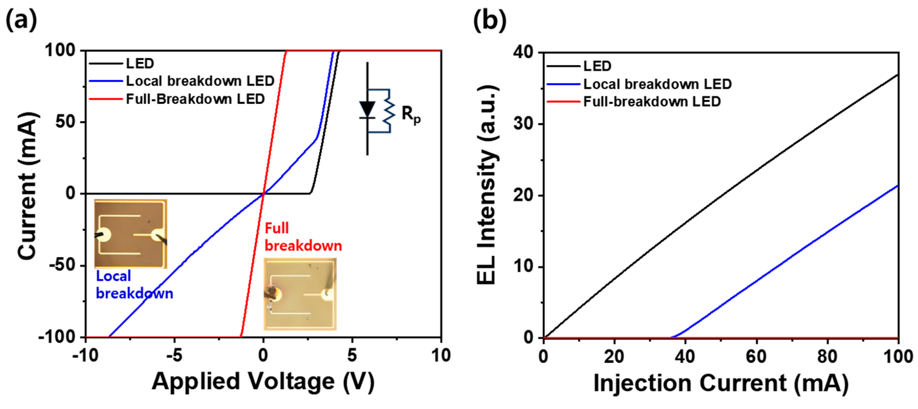
Figure 1a,b show the current–voltage (I–V) and current–light output power (I–L) curves of conventional GaN-based LEDs, illustrating different breakdown conditions, respectively. The LED without any breakdown process exhibits typical diode behavior, with a turn-on voltage of 2.8 eV, very low reverse leakage current and an operation volage of 3.0 V at 20 mA. After forming a full breakdown at a reverse voltage significantly exceeding the typical breakdown voltage of approximately 60 V, LEDs that have undergone this full breakdown exhibit linear I–V characteristics. This phenomenon is characterized by the absence of electroluminescence (EL) and electrode damage that closely resembles burn-like shapes. This corresponds to the familiar breakdown phenomenon observed in GaN-based LEDs, depicted in the inset of
Figure 1a. However, after initiating a local breakdown process within the p-layer, the LED demonstrates I–V properties characterized by almost linear behavior reminiscent of a conductive material, existing below +3.4 V. Beyond this point, the LED exhibits normal I–V characteristics typical of GaN-based LEDs. The unique limited linear I–V behavior observed in the LED can be attributed to the formation of a local breakdown conductive channel analogous to a parallel resistance [
10]. This channel serves as an alternative path for n-type carriers, functioning akin to an n-type electrode. Owing to the presence of this parallel resistance induced by the local breakdown, the LED fails to emit EL emission at an operational current of approximately 40 mA, which signifies the transition position from conductive behavior to diode-like behavior, as illustrated in
Figure 1b.
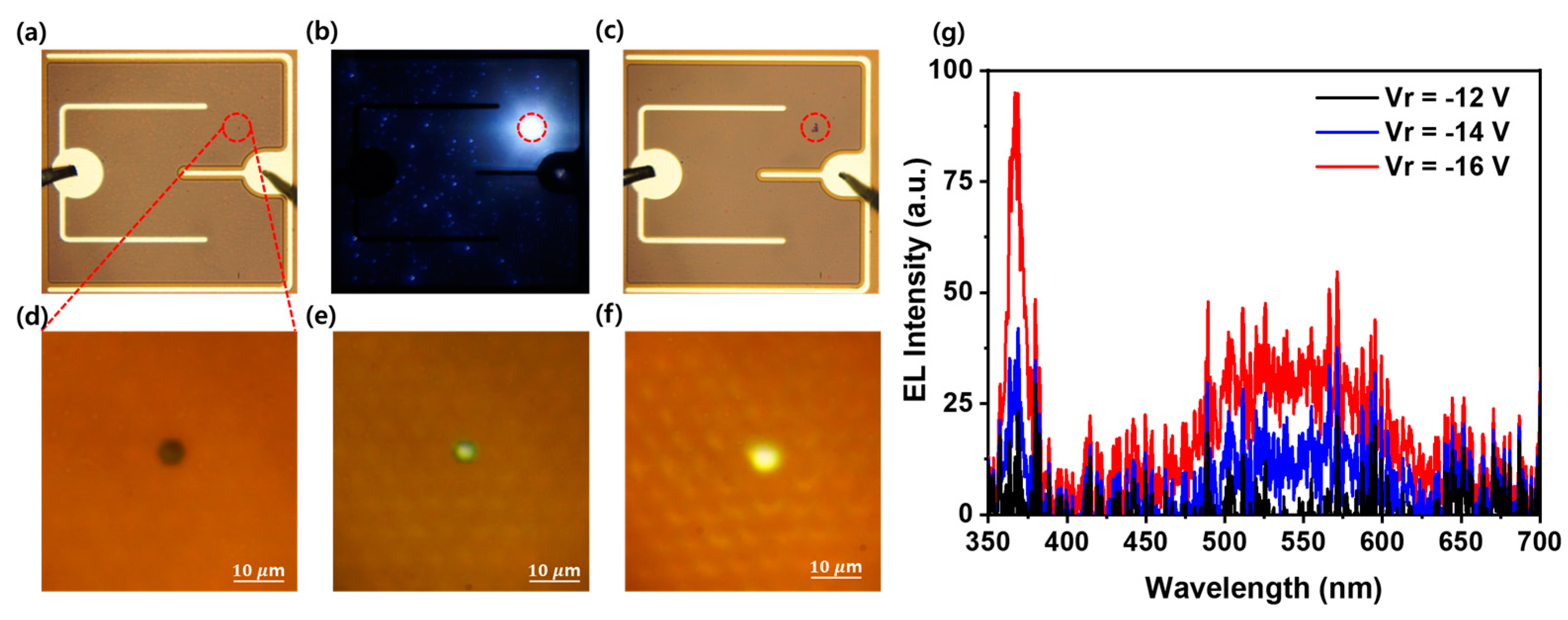
Figure 2a presents a photographic image of the LED before any operating current injection, revealing no surface damage and indicating a well-fabricated LED. Notably, a specific surface defect is enclosed in a red-dashed circular region, representing a very small-sized surface V-defect. This can be better observed in
Figure 2d, where a larger, magnified photograph is presented. This surface V-defect is known to result from the low surface mobility of adatoms during the low temperature growth of the InGaN layer [
11].
Figure 2b exhibits a reverse dot-like luminescence image of GaN-based LEDs, characterized by two distinct types of dot-like luminescence. These dot-like luminescence patterns are affected by crystal defect-related leakage currents [
29]. One type corresponds to the typical very-small-sized dot-like luminescence, while the other appears as the giant dot-like luminescence (GDL) confined within a red-dashed line circular region. This region aligns precisely with the position of surface V-defect, as depicted in
Figure 2b. In addition,
Figure 2a–c demonstrate that applying a high reverse bias induced local breakdown, and this local breakdown region closely corresponds to the regions exhibiting GLD and the surface V-defect region. Collectively, these results underscore the distinct luminescence behaviors and breakdown characteristics that emerge when comparing GaN-based LEDs with and without surface V-shape defects. LEDs without surface V-shape defects exhibit conventional dot-like luminescence, randomly distributed on the surface of the LED, and have a relatively lower emission intensity compared to LEDs with V-shape defects. Reverse breakdown sporadically occurs in these LEDs, independent of the presence of defects. In contrast, GaN-based LEDs with surface V-shape defects exhibit a remarkable luminescence phenomenon termed GDL. This luminescence exhibits a relatively higher intensity compared to the conventional dot-like luminescence observed in LEDs without surface V-shape defect. Crucially, the GDL is localized to the surface V-shape regions, emphasizing the pivotal role of these defects in enhancing luminescence. Furthermore, the breakdown behavior within LEDs with surface V-shape defects is different from that observed in LED without defects. In some cases, the local breakdown tends to specifically occur at the surface V-shape defects, potentially linked to the stress distribution in the V-shape defects. As shown in
Figure 2d,f, the presence of surface V-defects and the formation of reverse GDL are clearly observed in GaN-based LEDs. Notably, under reverse bias, emission images of GDL are observed at the surface V-defect using high-resolution optical microscopy. Initiated at the valley end of the surface V-defect at −12 V, the luminescence extends from the valley-end to the sidewall as the reverse voltage increases, as illustrated in
Figure 2d,f. These findings compellingly suggest that the generation of giant dot-like luminescence stems from the surface V-defects.
Figure 2g shows the EL spectra of GDL in a GaN-based LED under reverse bias ranging from −12 V to −16 V.
The EL spectra include two distinct peaks. One peak, at 366 nm, is attributed to the GaN film, while the other is a yellow emission that start weakly at 450 nm and extends from 500 nm to 600 nm. The reverse dot-like luminescence is known to be affected by a few factors such as the indium localization states and Mg doping level within the InGaN active layer [
29]. In typical reverse dot-like luminescence of a GaN-based blue LED, the primary EL peak is reported around 450 nm. However, in the case of GDLs, the EL spectrum exhibits a weak 450 nm and relatively strong yellow luminescence, which can be attributed to the high indium localizations in the V-defect regions. This occurrence demonstrates the potential of these defects to form a localized breakdown conductive channel within GaN-based LEDs. By observing the correlation between the GDL and the surface V-defects, it becomes possible to predict the potential location of local breakdown without the need to directly confirm the presence of surface defects on the LED using high-magnification microscopy under reverse bias conditions.
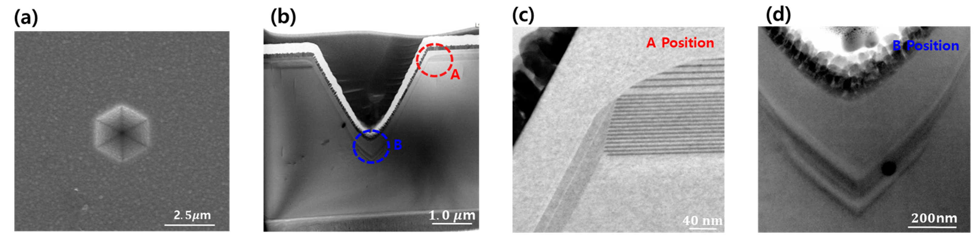
Figure 3a,b present TEM images of the surface and cross-section of the V-defect region within the GaN-based LED, respectively. These V-shape defects are known to form during the growth of the GaN film due to insufficient two-dimensional growth at the threading dislocations [
11]. These V-shape defects exhibit a six-plane {10–11} crystallographic structure. Upon detailed examination, two distinct positions within the V-shape defect emerged: denoted as positions A and B. Position A marks the starting region of the V-shape defect in the GaN-based LEDs, where the bending of the InGaN 5 QWs is evident. In this region, the InGaN QWs exhibit a configuration featuring a well-formed well layer at the top and an exceedingly thin well layer along the side of the V-shape defect. The variation in well thickness within the InGaN QWs at the top and sidewall stem from differing growth rates between the (0001) plane and the sidewall planes {10–11} [
14,
24]. On the contrary, at location B, the InGaN quantum wells (QWs) on both sides converge, resulting in an observed increase in well layer thickness at the bottom part of the V-shaped defect. Notably, a thicker and darker region emerges at the bottom edge where the lower hexagonal side faces meet, indicating that this thicker well layer is composed of a higher In composition compared to the well layer on the sides. Based on these observations, it can be inferred that the V-shaped defect initiates low-energy emission at a low reverse voltage, which first occurs at the bottom edge of the V-shaped defect due to the presence of a highly In-localized region at the bottom of the defect. Furthermore, it is believed that as the reverse voltage increases, the GDL forms by expanding from the bottom end to a thin well layer located on the sidewall, as shown in
Figure 2d,f.
To evaluate the relationship between the stress of surface V-shape defect and the local breakdown phenomena, micro-Raman analysis was performed, as shown in
Figure 4. In general, the Raman E
2 (high) peak of the free-standing GaN film is known to be a 568 cm
−1 [
30]. However, the Raman spectra for regions with and without V-defects in GaN-based LEDs, as shown in
Figure 4a, exhibit peaks ranging from 570.16 cm
−1 to 570.7 cm
−1. This indicates that, irrespective of the presence of surface V-defects, the GaN films experience compressive stress, primarily because of their larger lattice constant compared to the c-plane sapphire substrate. In addition, the surface V-shape defect regions in these LEDs exhibit a Stokes shift, which deviates from the behavior observed in the normal region with a V-shape defect in conventional GaN-based LEDs. Specifically, the Raman shift for the normal region in GaN-based LED is measured at 570.7 cm
−1, whereas the Raman shift within the V-shape defect region is found to be slightly lower, at 570.16 cm
−1. This difference in Raman shift indicates a change in the vibrational mode of the material, which is potentially due to a change in the crystal structure or composition within the V-shaped defect region. As the Raman peak information mainly stems from the top p-GaN film grown on the InGaN active layer, primarily due to the limitation of laser penetration depth, the shift in the E
2 (high) peak predominantly reflects the relative tensile stress experienced by the p-GaN layer grown atop the InGaN active layer, characterized by a larger lattice constant than the GaN film. In particular, compared to the non-surface V-defect region, the Raman Stokes shift suggests that the surface V-shaped defect region undergoes relatively tensile stresses compared to other regions of the LED, as depicted in
Figure 4a. This heightened tensile stress is induced by the presence of a region with a high In composition beneath the V-defect, as illustrated in
Figure 3d. In addition, the Raman spectra observed at the different positions within the V-shape defect in GaN-based LEDs reveal interesting variations in the Raman shift, as shown in
Figure 4b,c. The lowest Raman shift is obtained at the center region of the V-shape defect, and the Raman shift increases with positions towards the outer edges of the V-shape defect. This implies that the center position of V-shape defect exhibits the highest Stokes shift, leading to the highest tensile stress compared to other regions. These findings are consistent with the results of TEM, which exhibit a high In composition in the lower region of the V-shape defect, as shown in
Figure 3. Moreover, the Raman Stokes shift was found to increase slightly with the diameter of the surface V-shape defect, as shown in
Figure 4d. This observation suggests the possibility that the tensile stress may increase with the size of the V-shape defect.
The increase in tensile stress of the top p-type GaN layer is likely related to the concentration of indium content in the InGaN active layer at the bottom region of the V-shape defect. An increase in the size of the V-defect corresponds to an increase in the depth of the surface V-shaped defect. This occurs because the sidewall faces of the V-defect maintain a consistent crystal plane {1–101}. Consequently, larger and deeper V-defects contain a greater number of InGaN active layers, implying that more indium-rich regions can be formed at the bottom of the V-defect. The presence of indium-rich regions introduces strain to the adjacent material, leading to relatively higher tensile stress in the V-shape defect region. However, the weak correlation between the Raman peak and the V-defect size suggests that the small area at the bottom of the V-defect, relative to the beam size of the Raman laser, results in significant scattering of the Raman peak. Nonetheless, the distinct difference in Raman peak shifts between the V-defect and non-V-defect regions, as well as the results regarding the peak shift within the V-defect, may represent a critical factor influencing the optical and electrical characteristics of GaN-based LEDs under reverse bias conditions.
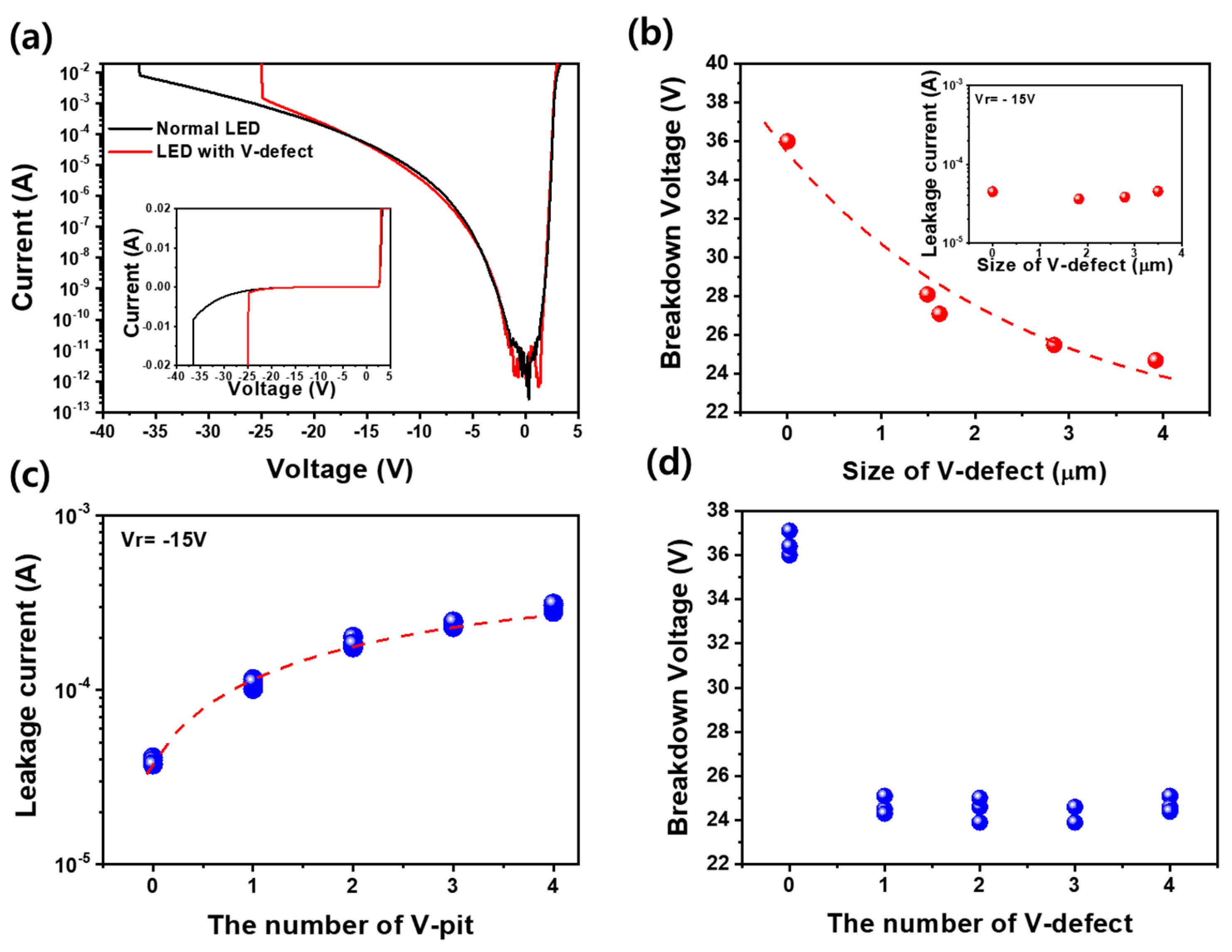
Figure 5a exhibits the log (I)−V curves of GaN-based LEDs with and without a surface V-defect. Remarkably, regardless of the presence of surface V-shape defects, the forward operation current and the reverse leakage current remain nearly identical. However, LEDs with surface V-shape defects exhibit slightly higher reverse leakage current compared to those without, prior to the onset of breakdown. Notably, the breakdown voltage of LEDs with surface V-shape defects is much lower than that of LEDs without surface V-shape defects. Conversely, the breakdown current for LEDs with surface V-shape defects is lower than that for LED without V-shape defects before the occurrence of breakdown. These observations strongly suggest that the surface V-shape defect plays a significant role in increasing the leakage current near the breakdown voltage, thereby accelerating the onset of breakdown and consequently leading to a reduction in breakdown volage. This phenomenon is likely attributed to the heightened tensile stress localized around the V-shape defect, as illustrated in
Figure 4c. In contrast, LEDs without V-defects that contributed to tensile stress are anticipated to exhibit higher breakdown voltage and breakdown current. In addition, to evaluate the effect of V-shape defect sizes and quantities on reverse leakage current and breakdown voltage, I–V measurements were conducted on GaN-based LEDs with various V-shape defect sizes and quantities, as depicted in
Figure 5b–d. The presence of surface V-shape defects significantly affects the electrical characteristics of GaN-based LEDs, particularly under reverse bias conditions. In
Figure 5a, the previously shown results indicate that the leakage current with and without the V-shaped defect appeared quite similar. This consistency aligns with the observation from the inset in
Figure 5b, which demonstrates that the reverse leakage current at −15 V is not significantly affected by the increased size of the surface V-shaped defect. This phenomenon is believed to have an insignificant effect on the leakage current since the size of the V-shaped defects is primarily determined by the low mobility of the adsorbed atoms, and the threading dislocations, which are responsible for the formation of V-shaped defects [
6], do not increase in number as the size of the V-shaped defects grows. As a result, the source of leakage across the n-p junction plane does not substantially increase at this reverse voltage region. However, as depicted in
Figure 5b, it is evident that the breakdown voltage of the LED decreases with the increasing size of the V-shaped defect. This phenomenon occurs because, as the V-shape defect enlarges, more indium-rich regions form at the bottom, facilitating carrier tunneling due to the development of larger localized tensile stress. Consequently, this escalation leads to higher leakage current, culminating in the generation of GDL and ultimately accelerating local breakdown. Furthermore, as shown in
Figure 5c,d, the reverse leakage current increases with the number of V-shaped defects, while the presence of V-shaped defects significantly decreases the breakdown voltage. Notably, the breakdown voltage is not significantly influenced by the number of V-shape defects. The reverse leakage current increases slightly with the presence of surface V-shape defects because the number of these defects is influenced by the number of threading dislocations, which can subsequently increase the reverse leakage current [
15]. However, even if there are multiple V-shaped defects on the LED surface, the localized breakdown occurs only in one V-shaped defect. Moreover, it is confirmed that even if the number of V-shaped defects increases, the breakdown voltage does not change significantly with the number of V-shaped defects because the breakdown phenomenon occurs preferentially in the V-shaped defect with the largest size, as shown in
Figure 5b, because the larger the V-shaped defect, the lower the breakdown voltage. This is because the local breakdown phenomenon occurs only in the V-shaped defect that is most susceptible to breakdown, particularly the one subjected to the highest tensile stress. This phenomenon explains why the breakdown voltage, which is about −36V in the absence of V-shaped defects, decreases significantly to −24V to −25V in the presence of V-shaped defects, as shown in
Figure 5d, but is almost unaffected by an increase in the number of V-shaped defects.


