1. Introduction
Since the first synthetic diamond was obtained in a laboratory [
1], diamonds produced in high pressure high temperature (HPHT) processes and later in chemical vapor deposition (CVD) processes steadily occupied new application areas. The unique properties of this crystal make it one of the most promising materials for radiation detectors [
2], heat sinks [
3], photonic mediums [
4,
5], Raman lasers [
6], information storage [
7], etc. Quite recently, nitrogen-doped diamonds were shown to operate effectively as photoconductive antennas (PCA) emitting terahertz (THz) pulses under 400 nm femtosecond pumping [
8,
9]. In light of the record dielectric strength and thermal conductivity, diamond seems a prospective candidate for high-power and high-intensity THz emitters.
In PCA, the THz wave results from a high photocurrent produced by photo-excited carriers and a strong external electric field [
10]. One of the key issues which has to be solved is the formation of conductive electrodes in the diamond bulk, terminals of a high voltage capacitor forming this field. Surface conductivity of an untreated diamond is relatively high, and, for instance, in the experiments described below, the threshold for a surface breakdown was comparable to that of air
kV/cm. Therefore, burying these electrodes in a substrate is of great importance because this the only way to realize the extra high magnitude of the breakdown field in the diamond bulk. The technique of creating encapsulated electrodes in a diamond should be robust and flexible, enabling us to design wide aperture antennas with numerous small gap (∼10
m) capacitors. Surface small-scale electrodes were applied and tested in the first diamond THz emitter [
11], while the buried ones have not yet been performed.
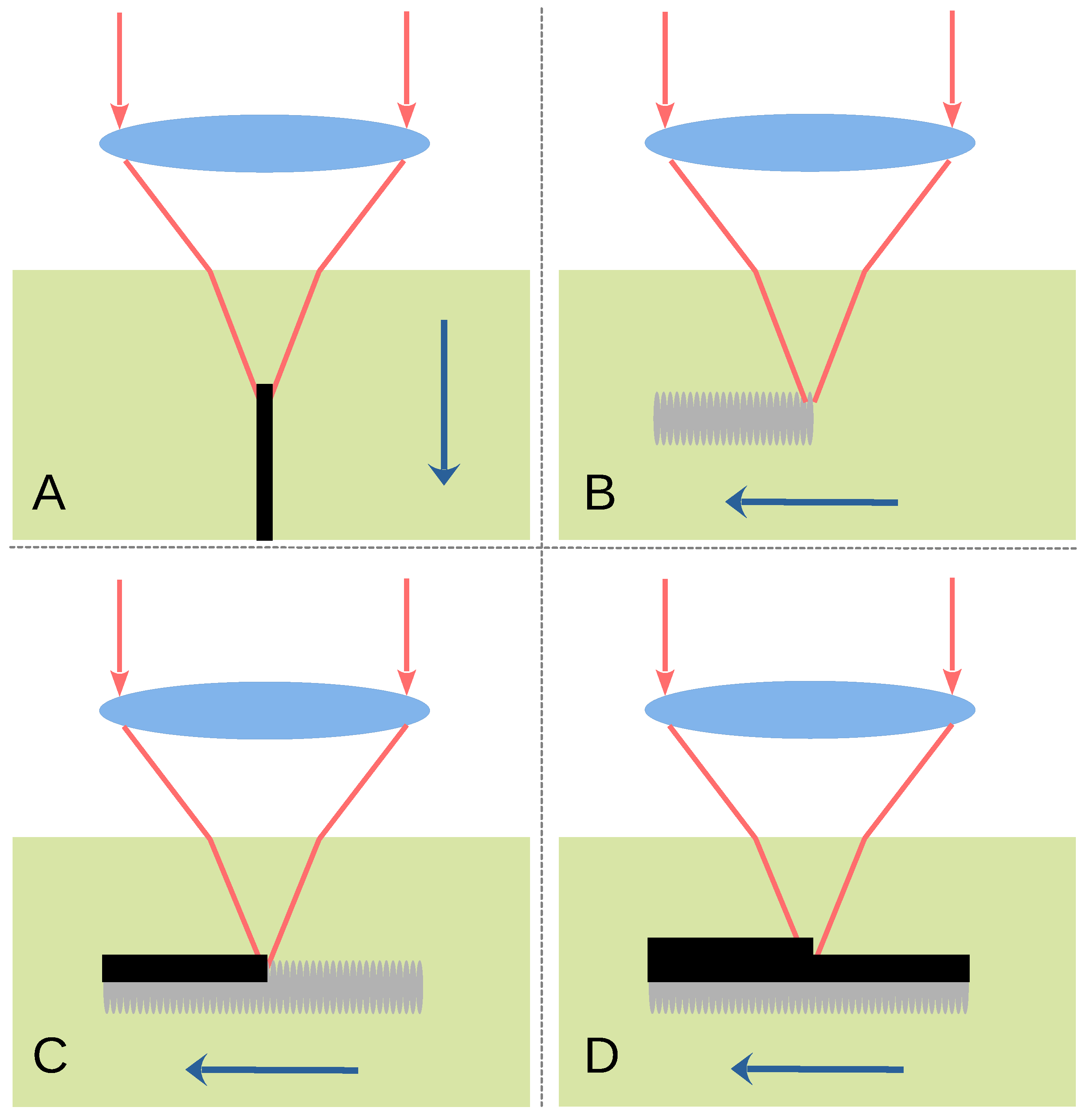
Usually the introduction of conductive wires into a dielectric substrate is a complex problem. Fortunately, in the case of diamond, its -coordinated structure is metastable and can be transformed into a -coordinated graphite-like structure as a result of some exposure, in particular, to intense laser irradiation. Diamond is transparent in a wide range of wavelengths, and to produce a lattice damage, the laser beam is focused on a micron-sized area. If the radiation intensity in the laser waist is high enough, a nonlinear absorption initiates a whole chain of local events, including diamond ionization and plasma cloud formation, relaxation of excited carriers, lattice heating, and, eventually, the diamond to graphite transition. The conductive pattern, which should be created in the crystal for the specific application, results from a coordinated combination of the local graphitization and the motion of a laser focus over the substrate.
In essence, the above model describes the interaction of an intense optical field with any transparent material, but diamond possesses a quite specific peculiarity, which strongly affects laser microstructuring of its bulk. The fact is that in contrast to diamond, the graphite-like phase is not transparent and absorbslight in a wide range of the spectrum. Thus, having once been produced, the graphite significantly enhances the optical absorption. In these conditions, the continuous irradiation makes the “graphitization wave” propagate toward the beam even without a focus translation [
12]. On the one hand, the propagation of the graphitization wave can be made coherent with a focus motion along the laser beam, producing a thin graphitized thread without gaps (
Figure 1A) [
13,
14]. On the other hand, the graphitization wave strongly interferes with control of the phase transition in a desired point under other scanning directions [
13]. This is especially true for perpendicular scanning, which at any laser fluence tends to produce dashed and unstable graphitized structures. As even a single gap disrupts wire conduction, such a structure can hardly be used as the electrode in the diamond-based THz antenna.
Several attempts were made to overcome this problem [
15,
16]. All concentrated on ultratight focusing to diminish the amount of laser energy necessitating the development of the nonlinear breakdown in diamond and simultaneously minimizing the optical field beyond the beam waist. Such an approach was found on the whole to be effective, however, technically sophisticated as it encounters huge aberrations which have to be completely eliminated. In this work, we search other solutions that can facilitate decreasing the effect of propagation of the graphitization wave and make 3D processing of diamond more flexible and stable.
2. Experiment
In the proper regime of direct laser writing, the laser-induced modification of material should always be located inside the laser focus. As was already mentioned, in the diamond, this condition is not met due to a jump of diamond–graphite absorbance. The graphitization threshold radically changes depending on the processing stage: the optical breakdown of the original diamond arises at
J/cm
, while the growth of the already arisen thread requires
J/cm
laser fluence. Consequently, if the laser fluence is close to the
threshold, no graphitization of the original diamond even starts. If the laser fluence exceeds the
threshold, after the optical breakdown, the graphitization wave moves toward the laser beam and easily leaves the laser waist [
17]. However, the longitudinal scanning allows providing the exact correlation of the graphitization wave motion and focus translation and, thus, a stable formation of the graphitized thread (
Figure 1A) [
13]. In contrast, the transverse scanning necessitates the distance which the graphite front can move along the beam be minimized (ideally to zero).
For this purpose, the processing routine was proposed to be divided into two steps: the seed damage formation (
Figure 1B) and the graphitization of the damaged bulk (
Figure 1C,D). The seed formation was carried out at high laser fluence and followed one key condition: no overlapping of laser shots during the transverse focus translation was allowed in order to avoid the development of a graphitization wave. The seed occurrence was thought to remarkably decrease the threshold of diamond graphitization. The second stage consisted of a low fluence, slow and repetitive scanning along the same trace as the seed stage. This stage should produce a stable formation of the graphitized thread (
Figure 1C) and its sequential thickening (
Figure 1D).
The experimental setup is shown in the
Figure 2. Diamond processing was performed using a fiber laser (Huaray, Hangzhou, China), emitting femtosecond (
fs) IR (
nm) pulses with a 750 kHz repetition rate. The pulse energy was
J. Only a small part of this value was utilized for processing: the pulse energy was decreased and controlled with a half-wave plate and a Glan polarizer. The repetition rate was also decreased to 100 Hz in order to provide an online record of graphitized structure formation. The beam was focused with a high-power objective (50X, 980–1130 nm, NA = 0.65, Thorlabs, Newton, NJ, USA) which was equipped by manual correction of spherical aberrations. The Gaussian beam radius in the focal plane was ≈0.5
m at the
level. After adjustment of a correction collar, the threshold of optical breakdown was very close to a constant (∼1.0
J) in the range of 50
m to 350
m beneath the diamond surface. As a matter of fact, this range determines a region size where laser writing could be realized without the readjustment of the correction ring. The graphitized structures described below were produced at a ∼100
m depth beneath the surface. The Rayleigh length of the beam focused in the diamond was evaluated to be 5–7
m. The laser pulse energy varied in the ranges of
J for the seed damage and
J for the graphitization stage. The images of graphitized structures were written from pulse to pulse with a long distance objective (NA = 0.4, Mitutoyo, Kawasaki, Japan) and CMOS camera (Thorlabs, Newton, NJ, USA). The zone processed was illuminated by white LED in the transmitted light mode (
Figure 2).
A commercial single-crystal diamond substrate (≈3 × 3 × 0.5 mm, Infi Advanced Materias, Shanghai, China) obtained in an HPHT process was used for the laser treatment. Nitrogen content characterized by means of absorption spectroscopy was about ∼20 ppm. A 3 × 3 mm face had a (100) orientation, while other sides had a (110) orientation. All six faces were mechanically polished for better imaging of the structures produced inside the crystal. The sample was fixed on the 3D electro-mechanical stage driven by DC servo motors (Newport, RI, USA). The graphitized structures were made translating the diamond sample in a vertical direction. Such a configuration enabled creating the threads perpendicular to the laser beam axes and watching this process in situ through a side of the sample (
Figure 2).
3. Results and Discussion
Figure 3 depicts the typical graphitized structures arisen in the diamond crystal under laser focus scanning in the direction perpendicular to the laser beam (here, in the vertical direction). The first regime shown (
Figure 3a) exemplifies processing without the seed stage (pulse energies in the seed and graphitization stages are equal:
). The
value in the case was high enough and produced discernible although unstable black traces over the scanning length. It is clearly seen that the structure created after the first passage, when the different shots did not interfere with each other, was quite straight. In contrast, the second passage thread tends to belt toward the laser beam. This is an expected consequence of the graphitization wave effect. Note that repetitive scanning resulted in the clear thickening of the graphitized structure but simultaneously produced point cracks which stimulated the growth of the elongated straightforward fractures oriented along the (111) diamond plane.
Figure 3b demonstrates a course of the seed-graphitization process (
). The main effect was that the graphitized thread stayed in the zone of seed damage; no tilt to the laser beam was found. It is of interest that after the first graphitization scan, the created structure was rather intermittent but in processing the gaps completely disappeared. So, even without an optimization, the repetition of the irradiation guaranties the formation of the continuous graphitized wire in the diamond. The wire also gradually increased in thickness. The (111) fractures were also revealed though they were much shorter than in the previous case.
The next example of the graphitized structures obtained in the seed-graphitization regime is shown in
Figure 4. The pulse energy in the seed stage was decreased, and the traces of diamond damage were not seen (first slide in
Figure 4). However, after the first passage in the graphitization stage, the straightforward continuous thread arose (second slide in
Figure 4). The thickening of the thread during all the next scans was quite effective and accompanied by relatively strong scattering of incident radiation on the graphite (third slide in
Figure 4). The geometry of the produced structure can be regarded as ideal in the initial scan; then it worsened, and clear splitting of the produced thread happened during the fifth scan.
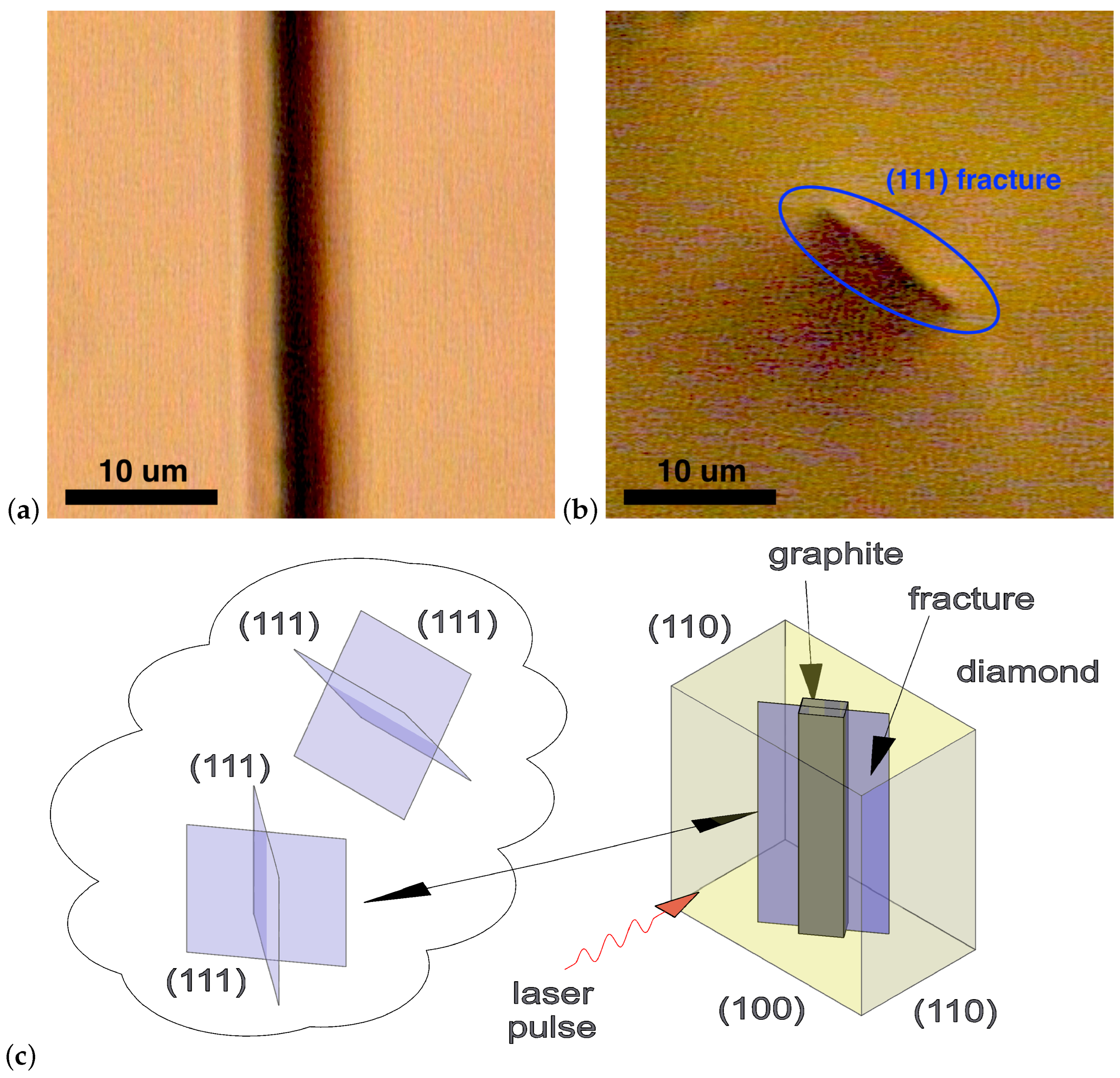
These structures were investigated in detail with a 100X objective laboratory bright-field microscope (Zeiss).
Figure 5a,b depict a lateral-side view and a top-side view of such a graphitized structure. The lateral-side image shows that besides a black graphitized thread, there is a transparent ribbon that is approximately three times wider. This ribbon looks like a cleavage around the graphitized wire. The clearest picture of an exact geometry of the produced thread is given by its top-side image.
Figure 5b undoubtedly indicates the occurrence of a wide and thin fracture along the (111) crystal plane. It should be emphasized that the graphitized phase is localized inside this fracture; i.e., the graphitized thread is not really a “thread”, which inherently has a cylindrical shape. but a flat ribbon.
Figure 5c illustrates the suggested cleavage-driven graphitization process in the diamond bulk. Laser graphitization is a well-known source of microfractures in diamond bulk [
18]. The main reason of diamond cracking is a difference in mass density of graphite and diamond. Upon the diamond–graphite transition, the graphitized phase tries to expand and disrupts a surrounding crystal. The fracture net created in diamond can be quite ramified or contain only a single extended fracture [
18], but the cleavage always happens in the (111) crystal plane. It is noteworthy that a cylindrical shape of graphitized threads produced in customary regimes, particularly, in the regime of graphitization wave, is deceptive. In fact, the threads consist of numerous of fractures filled by the graphitized phase [
18].
As shown above, the localization of the graphitized structure produced by the laser radiation was restricted by the seed region and thus coincided more or less with the laser focus scanning line. The key feature of the used configuration was that this line was in the (111) plane (
Figure 5c). In these conditions, the microfractures apparently merged and formed a dominant fracture which contained the graphitized ribbon inside.
The threads produced in this way were quite straightforward and continuous. This result proves that having been created, the cleavage supports and guides the graphitization process. The fracture escapes beyond the graphitized area, and laser radiation interacts with the walls of the fracture. These free surfaces, first, are of a low graphitization threshold; therefore a relatively low laser fluence can initiate graphitization of a new portion of diamond. Second, the created graphite expands inside the fracture, inducing its growth from pulse to pulse. Perhaps, in the presence of the dominant fracture, it is irrelevant whether the seed structure exists or not. Note here also that the orientation of the crystal face was shown to play an important role in the surface graphitization process [
19]. As graphitization preferably proceeds via the transformation of two diamond (111) planes into the graphite (0001) plane, the graphitized layer which is produced on the (111) face is much closer to the highly oriented graphite than that produced with the laser on other faces.
As was already mentioned, the possible application fields of the buried threads cover a wide variety of electronic devices, including photoconductive antennas, detectors of ionizing radiation, etc. There are two major requirements which produced graphitized electrodes should satisfy as far as possible. The first one is high conductivity; the second is an intact surrounding diamond matrix, and the second is more important because the high conductivity is vitally significant for only high-speed devices, while the possible electronic-active defects interfere with current flows at any operation frequency. Future studies should investigate both aspects.
To this moment, the resistivity of a graphitized zig-zag fracture produced by nanosecond pulses in diamond was found to be close to the resistivity of polycrystalline graphite [
20]. The conductivity of the cleavage-driven graphitized threads is expected to be even higher due to the higher structural perfection of the graphite produced. The information about the structural defects in the vicinity of the laser-produced conducting phase is rather limited. We know only a few works encountered this problem [
21]. However, some deterioration of operation of the diamond-based detectors was attributed to the presence of electronic traps located in regions close to electrodes [
22]. The degree of the diamond damage in the cleavage-driven process should be studied and compared with the damage induced in the customary regime of graphitized thread formation.
At this time, the development mechanism of cleavage-driven graphitization is rather unclear and needs further investigation. There are obvious questions. For instance, how can we obtain guaranteed cleavage along two of four (111) planes (see
Figure 5c)? What parameters of laser irradiation (pulse energy, pulse duration, beam aperture, scanning speed) provide a stable evolution of the dominant fracture?
Here, we performed a preliminary optimization of cleavage-driven processing and found the ranges of laser energies applied in the seed and graphitization stages that provide formation of the graphitized threads in diamond. The scanning speed in the seed stage was fixed: the average pulse number per point was one in order to avoid the graphitization wave toward the beam. The scanning speed in the graphitization stage was also fixed: the average pulse number per point was around four, providing strong overlapping of laser shots. The seed energy, i.e., the pulse energy in the seed stage, was limited by a range around a single pulse graphitization threshold: . At the low end of this range, the laser produced no visual traces in diamond. In contrast, at the high end, the irradiation resulted in well-distinguished spots in the bulk of the crystal. The graphitization energy, i.e., the pulse energy in the graphitization stage, varied in a much wider range. The maximum was around the single pulse threshold: . The minimum was around the multiple pulse threshold of the damaged diamond graphitization: .
The results of processing were separated into three groups: (1) the graphitized structure was absent, (2) the structure was dashed, and (3) the structure was continuous. As is evident in the data in
Figure 6, these groups strongly correlated with the irradiation energy. At the low energy, no graphitization started, as expected. Moderate energies in the graphitization stage caused unstable writing in the bulk, and energies close to the seed stage energies (
) led to continuous structuring. Taken as a whole, the stable graphitization was shifted toward the high seed energies. This preliminary optimization demonstrates the existence of a wide range of laser pulse energies at which the buried graphitized threads can be obtained at the perpendicular scanning manner. Note that the quality of graphitized wires implies many aspects besides the continuity and includes uniformity, free cracking defectiveness, straightforwardness, etc. These aspects are not reflected in
Figure 6 and require further study.
4. Conclusions
In conclusion, this work studied the process of laser graphitization at the transverse focus translation through the diamond bulk and demonstrated that even under relatively moderate focusing, the undesirable motion of the graphitization wave can be suppressed. Two main mechanisms were found to restrict the propagation of the graphitization front toward a laser beam.
The first one is a high fluence local damage of diamond, which works as a seed and decreases the local threshold of diamond graphitization sharply. Preliminary single shot 3D processing of the diamond bulk enables the subsequent graphitization at a low laser fluence and prevents the development of graphitization in the undamaged zones. The developed routine of double processing allows repetitive laser irradiation which heals the defects of continuous graphitized wire and increases its thickness. On the other hand, this regime is not quite stable and requires an optimization of laser and scanning parameters. The continuous structures were produced at the seed energy which is close to the threshold of the single pulse graphitization (∼1.1 J) and at a graphitization energy ranging from ∼0.2 J to ∼1 J.
The second mechanism, having been turned on, provides stable processing without any wire gap. It consists of the formation of the dominant fracture oriented in the (111) plane and drives the development of the graphitized thread inside this fracture. This cleavage-driven regime also allows thickening the graphitized thread. The dominant cleavage in diamond seems to be initiated, in turn, by the seed-graphitization process, and in our view, the 3D laser writing in diamond should exploit both the mechanisms.
Future work will focus on a control of diamond cleavage, investigation of the lattice structure, and electronic properties of the graphitized phase localized inside the laser-induced fracture. Our findings enhance the potential of 3D laser processing of diamond bulk and give rise to building extremely biased diamond THz antennas.

 ,
, 


