Article

High-Speed Laser Cutting Silicon-Glass Double Layer Wafer with Laser-Induced Thermal-Crack Propagation

1
Guangdong Provincial Key Laboratory of Micro/Nano Optomechatronics Engineering, College of Mechatronics and Control Engineering, Shenzhen University, Shenzhen 518060, China
2
New Display Technology and Equipment Center, Jihua Laboratory, Foshan 528200, China
*
Author to whom correspondence should be addressed.
Processes 2023, 11(4), 1177; https://doi.org/10.3390/pr11041177
Submission received: 3 March 2023 / Revised: 29 March 2023 / Accepted: 4 April 2023 / Published: 11 April 2023

Abstract

:
This paper studied laser induced thermal-crack propagation (LITP) dicing of a glass-silicon double-layer wafer with high scanning speed. A defocusing continuous laser was used in the experimental system as the volumetric heat source for the glass layer and the surface heat source for the silicon layer. Based on the principle of thermal-crack propagation, the commercial software ABAQUS was used on the simulated analysis, and the results of temperature field and thermal stress field distribution with high and low speed were compared. The experiment was executed in accordance with the simulation parameters. The surface morphology of the cut section was described by optical microscopy and a profilometer, and combined with the results, the non-synchronous propagation process of the crack under high speed scanning was revealed. Most importantly, the scanning section with a nanoscale surface roughness was obtained. The surface roughness of the silicon layer was 19 nm, and that of glass layer was 9 nm.

1. Introduction

It has been reported that glass-silicon bilayers are widely used in precision devices such as integrated circuits (ICs) and micro-electro-mechanical systems (MEMS) [1,2].
Knowles et al. described a process that involves connecting glass and silicon wafers through anodic bonding to encapsulate micro devices. This process ensures good reliability, stability, and gas tightness. Monocrystalline silicon is preferred over polysilicon for the wafers due to its superior mechanical and electrical properties [3]. Esashi et al. proposed a first level of packaging for these devices based on the wafer-level chip scale packaging (WLCSP) technology [4]. After the circuit deposition procedure, this method enables the combination of patterned glass and silicon wafers in a single step, which can then be shredded. Until now, finding a suitable, high-quality, and efficient dicing technology has been a pressing issue [5,6,7]. Conventional scanning of brittle materials is performed by means of a rotating diamond scanning wheel mounted on a mechanical cutter. The process involves the injection of coolant to cool the scanning area. Miyake et al. noted that left-handed coolant with chips and microcracks may weaken the edge strength and trigger the impending failure of the microdevice [8]. The limitations above-mentioned have significant implications for the productivity and yield rates. In order to improve the edge quality, further treatments such as water grinding are required. Due to these drawbacks, researchers have explored non-mechanical scanning techniques. In this regard, Riveiro et al. demonstrated that well-designed laser systems provide a viable alternative for cutting soda glass [9]. Laser scanning is a non-contact process that prevents tool wear and eliminates contamination. However, studies by Lindroos et al. have shown that conventional laser processing involves exposing the substrate to a highly intense focused laser beam, leading to thermal defects such as heat-affected zones and microcracks, which can be severe in the cut area [10].
Compared to other scanning methods, laser-induced thermal-crack propagation (LITP) appears to be a highly promising technique for scanning brittle materials [11]. Its most significant features include a low operating temperature (below 500 °C) and a zero-width scanning path (in full-body scanning mode) [12]. Lumley et al. were the first to propose the LITP-based scanning technique [13], and significant progress has been made in the industrial application of this technology over the past few decades [14,15,16]. Laser induced thermal-crack propagation (LITP) is the conversion of the bonded wafer into a form of thermal energy absorbed by multiphotons and transferred to the interior and borders of the sheet. This leads to an uneven temperature rise inside the sheet, creating a temperature gradient [17]. The temperature rise leads to the thermal expansion of the material, while the temperature gradient and the differences in the thermophysical properties of glass and silicon lead to inhomogeneous thermal expansion of the material, which results in thermal stresses within the material [18]. Compressive stresses appear in the region near the laser point, while tensile stresses appear in the region near the laser point. Next, prefabricated cracks in the material expand in response to the tensile stress, and as the cracks expand step by step, the elastic energy is released as surface energy. As the laser beam moves, the energy is absorbed and converted, and the crack continues to grow, scanning the material [19,20].
CAI Yecheng et al. proposed an effective three-dimensional model to calculate the principle of the thermal action of laser-induced thermal-crack propagation in scanning glass/silicon bonded wafers at low velocities [21]. The results illustrate the crack propagation process in the laser-induced thermal-crack propagation (LITP) scanning of bilayer wafers at low velocities and apply the laser-induced thermal-crack propagation (LITP) technique to the field of silicon-glass bonded double layer wafer dicing.
The issue of processing efficiency is a challenge that the laser-induced thermal-crack propagation (LITP) technology cannot overcome [22,23]. Increasing the scanning speed is the most direct and effective method to improve processing efficiency. In this regard, finite element simulation using the commercial software Abaqus was performed to analyze the scanning mechanism of laser high-speed-induced thermal cracking in glass/silicon bonded wafers. Optical microscopy and profilometer were used to observe the surface morphology of the scanned path and determine the asynchronous expansion and crack propagation mode of the glass and silicon layers. Based on these results, a comparison between high-speed and low-speed laser-induced thermal cracking scanning revealed that better cross-sectional quality could be obtained at high laser speeds. This study provides a solution for improving production efficiency in laser-induced thermal-crack propagation (LITP) processing, which can be more widely used in various fields, but also has limitations: the technology is currently only available for processing with brittle materials.

2. Materials and Methods

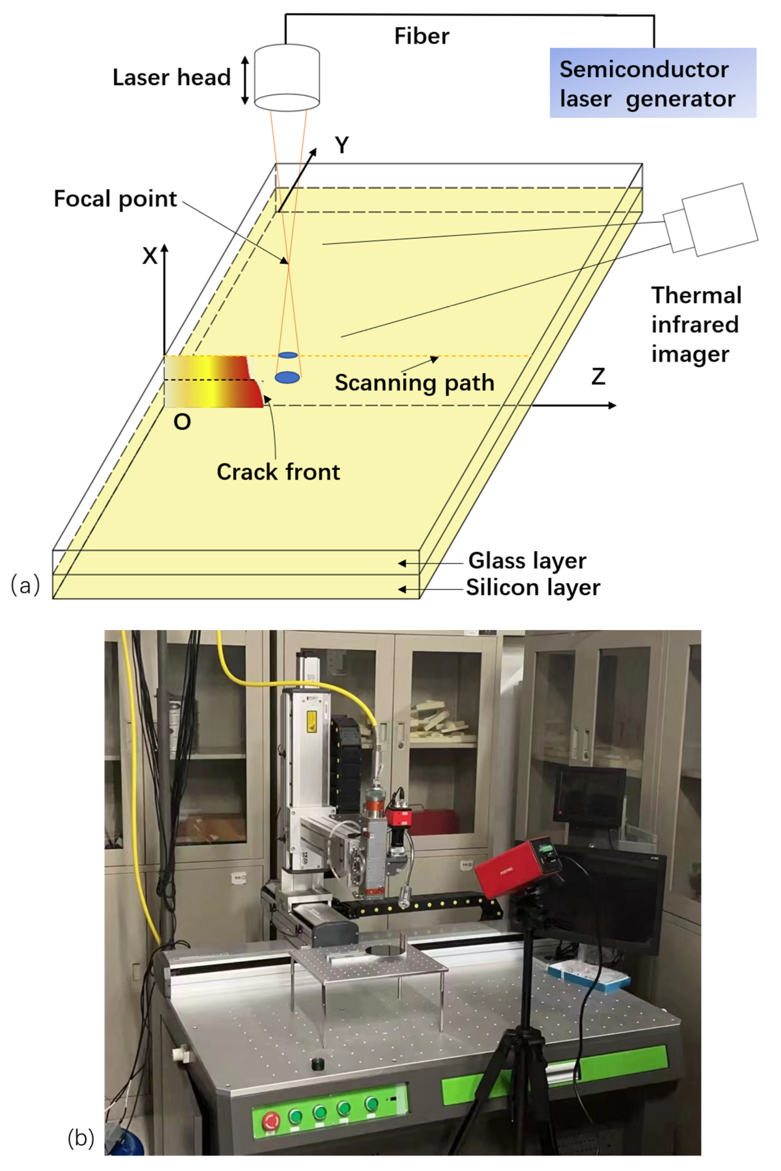
2.1. Experimental Procedure

Figure 1 shows the schematic diagram of the experimental setup used for dicing a glass-silicon double layer wafer based on LITP. The experiments were carried out at an ambient temperature of 20 °C using a continuous fiber-coupled semiconductor laser source that emits at 1064 nm in the TEM00 mode, with a maximum output power of 300 [24,25]. The laser head emitted a highly concentrated beam of light that was directed vertically onto the surface of the specimen being processed, ensuring precision and accuracy during the processing. The specimen was firmly fixed onto the X-Y positioning table to guarantee its accurate alignment and positioning during the process. The operating system plays a crucial role in determining the processing position of the specimen, ensuring that the laser beam is directed precisely to the desired location. Additionally, the laser head can be adjusted to control the Z-axis direction, allowing for the processing of materials at varying depths and thicknesses.
The samples were formed by combining a boron float 33 borosilicate glass wafer, manufactured by Schott, with an anode made of an n-type silicon wafer featuring (100) crystal planes. The prototype bonding and depletion layers measured between 2 and 20 nm and 1 µm, respectively. The silicon and glass wafers had a thickness of 0.5 mm and a diameter of 101.6 mm (4 inches). Prior to sample processing, an initial crack was made through the thickness, approximately 1 mm deep, using a diamond wire saw at the designated processing position.
The specimen was secured onto the X-Y stage with the glass side facing the laser head, and the scan path was programmed through the CNC operating system. The laser scanning parameters used during the experiment are detailed in Table 1. The cut surface was then examined under an optical microscope (Axiovert 200, Zeiss, Oberkochen, Germany), while the crack edge profile and surface roughness were measured using a surface profiler (PGI Dimension, Taylor Hobson, Leicester, UK).

2.2. Theoretical Approach

The thermal stress field was meticulously computed, and the crack propagation process was simulated by utilizing the commercial software ABAQUS finite element analysis. To provide a comprehensive understanding of the numerical analysis, below are the fundamental assumptions and simplifications summarized.
  • The material distribution of glass and silicon layers was uniform and flawless; both the glass and silicon layers were isotropic in thermal analysis, while in the stress analysis, the glass layer was isotropic and the silicon layer was anisotropic, unlike other layers.
  • The glass-silicon double wafer anode bond layer was free of any defects; the friction problem and heat transfer between the sample and the fixture during the scanning process were ignored. Since the thickness of the bond layer was extremely small (2–20 nm) and can be considered zero, the gravitational and residual stresses after anode bonding could also be neglected.
  • All parameters were ignored or set to zero except for the process parameters, influencing factors, and material parameters considered in the simulation such as beam quality factor, etc.
On a macroscopic level, the process of low-intensity heat action aligns with Fourier’s law of heat transfer. By applying Fourier’s law and the first law of thermodynamics, the heat transfer issue can be analyzed. The 3D instantaneous heat conduction differential Equation (1), in the right-angle coordinate system, provides the 3D temperature distribution T (x,y,z,t) based on the given initial and boundary conditions.
x λ · T x + y λ · T y + z λ · T z + q ˙ = ρ c · T t
T | t = 0 = T 0
k T z Ω = h T T + σ ε T 4 T 4  
T | i n G = T | i n S i
where λ is the thermal conductivity; T is the temperature; q ˙ is the heat flow density of heat source; ρ is the density; c is the heat; t is the time. The initial temperature   T 0 represents the outside room temperature; Ω is the boundary surface of regional Ω ; n is the outer normal direction of Ω ;   σ   is the Steffen–Boltzmann constant with a value of 5.67 × 10 8 W m 2 · K 4 ;   ε   is the emissivity or total energy emissivity, which takes values between 0 and 1; h is the convective heat transfer coefficient. The density of glass is 2230 Kg / m 3 and the density of silicon is 2329 Kg / m 3 .
In order to solve Equations (7) and (8), it is necessary to establish a mathematical formula to describe the thermal source distribution when a silicon glass bilayer wafer is irradiated by laser. This process occurs simultaneously at the air–glass interface and the glass–silicon interface, where some energy is reflected, some is absorbed, and the rest is transmitted. Table 2 and Table 3 provide the refractive indices of BF33 glass and silicon at 1064 nm, taking into account the refractive index of air at room temperature (20 °C). Using Equations (5) and (6), the normal incident reflectivity R A G (refractive index from air to glass is 1.474) and R G S i (refractive index from glass to silicon is 3.550) were calculated to be 3.67% and 17.1%, respectively. It should be noted that the energy reflected from the silicon surface is absorbed by the glass layer. Therefore, when calculating the total absorption coefficients of the glass and silicon layers, this energy must be considered and corrected according to the experimental data. The corrected values were 0.392% and 79.61%, respectively.
R 12 = n 1 n 2 2 / n 1 + n 2 2
I z = I 0 e α z
Therefore, the process of laser irradiation was utilized as a source of heat that spreads throughout the entire volume of the glass layer, while acting as a source of heat only on the surface of the silicon layer, as depicted in Figure 2. The mathematical expressions for the volume heat flux q G and surface heat flux q S i are described using Beer–Lambert’s law and the Gaussian distribution of laser energy, which are presented as Equations (7) and (8), respectively.
q G x , y , z = 2 1 R A G α P 0 π r G + H G + H S i z t a n θ / 2 2 · e α · H G + H S i z · e 2 x x 0 v t 2 y y 0 2 r G + H G + H S i z t a n θ / 2 2
q S i x , y = 2 η s i P 0 π r s i 2 e 2 x x 0 v t 2 y y 0 2 r s i 2
where x 0 , y 0 are the position coordinates of the scanning start beam center; q G   is the heat flux function of the bulk heat source in the glass layer;   q S i is the surface heat source heat flux function of the silicon layer; R A G represents the reflectance of 1064 nm laser incident on the air-glass interface; P 0 is the laser power; H G , H S i are the thickness of the glass layer and silicon layer, respectively; r G , r S i are the spot radius of laser beam at the outer surface of glass layer and silicon layer, respectively;   θ is the divergence angle of the laser beam; v   is the scanning speed; η s i is the laser absorption rate on the silicon layer surface.
Equations (7) and (8) are established based on the global coordinate system used in the finite element model, describing the thermal energy generated by any node in the finite element model at any time point in the form of heat flux. The introduction of these equations enables dynamic time steps in the laser scanning process and provides more accurate and detailed analytical methods for studying the thermal distribution and energy transfer in laser processing. Furthermore, by considering the heat flux produced by each node in the finite element model, a deeper understanding of the physical processes and phenomena in laser processing can be achieved, leading to a more effective design and control of laser processing systems.
Figure 3 showcases a detailed representation of the specimen’s grid, which is composed of two distinct layers—a top layer of glass and a bottom layer of silicon. The unique properties of each layer necessitate a careful consideration of the mesh optimization strategy, as described in the subsequent text.
To optimize the mesh and ensure accurate simulation results, the two layers were divided into separate regions based on the laser scanning path and the maximum spot diameter, as detailed in [26,27,28]. The resulting mesh was finely tuned with a total of 140,211 nodes and 116,976 elements, providing a comprehensive and detailed analysis of the specimen’s behavior under different laser processing conditions.

3. Results

Figure 4 shows the finite element simulation results of the maximum history temperature at each point on the simulated scan line during the high-speed scan. From the time the laser spot did not enter the workpiece to the time it completely left the workpiece area, the whole scanning process took only 945.45 ms. During the high-speed scanning process, the maximum historical temperature at each point in the stable crack expansion stage varied within 0.2 °C with time, which was almost unchanged. The maximum historical temperature at each point on the interface layer was 348.77 °C, and the temperature difference value between the silicon layer and the interface layer was 41.69 °C compared to the outer surface of the silicon layer, which was 307.08 °C. The outer surface of the glass layer was only 121.26 °C, and the temperature difference value between the glass layer and the interfacial layer was 227.49 °C. The highest historical temperature on the scan line of the interfacial layer was only 443.52 °C. In addition, the lag time of the points on the outer surface of the glass layer with the same x-coordinate was 159.5 ms and the lag distance was 17.54 mm compared to the interface layer. Compared to this, the points on the outer surface of the silicon layer only lagged 5.0 ms and the lag distance was only 0.55 mm.
The simulation results of temperature fields on the upper and lower surfaces of the glass layer are presented in Figure 5a,b, respectively. Specifically, Figure 5a depicts the temperature distribution at low scanning speed (t = 13 s), while Figure 5c shows the temperature distribution at high scanning speed (t = 0.8 s). Upon the comparison of both figures, it was evident that the heat diffusion region caused by high-speed scanning was restricted to a small area near the bonding interface due to the low thermal conductivity of the glass. Furthermore, the temperature distribution on the upper surface of the glass layer lagged behind that of the interface layer and was relatively lower.
Figure 6c,d shows the temperature field and stress field distribution on the upper surface of the glass layer and the lower surface of the silicon layer at a high speed scanning time of 0.039 s. At this time, the laser spot center was located at the edge of the workpiece, and the maximum temperature of the workpiece was 322.6 °C, which had not yet reached the historical maximum temperature of 348.77 °C in the stable extension stage.
Figure 7c,d shows the temperature field and stress field distribution on the upper surface of the glass layer and the lower surface of the silicon layer at a high speed scanning time of 0.175 s. At this point, after the crack started at the cut entrance, the distance between the laser spot and the leading edge of the crack increased rapidly. The stress field distribution showed that the glass layer had the highest stress value near the interface, while the silicon layer had the highest stress value near the outer surface. This was basically consistent with the stress distribution and shape of the crack’s leading edge in the low-speed scanning, but the crack’s leading edge span was significantly increased.
According to Figure 6 and Figure 7, the results show that the temperature gradient along the thickness of the glass layer at the center of the laser spot was very large, which led to tensile stresses near the upper surface of the glass layer in this region, and the maximum tensile stress could even exceed 40 MPa. This stress distribution situation was the opposite of the compressive stress in the glass layer at the center of the laser spot under low-speed scanning.
Figure 8 shows that a shallow groove prefabricated with a diamond wire saw was visible at the edge of the sample crack initiation. A scalloped ripple line could be observed on the upper surface of the glass layer near the shallow groove, with the upper right corner as the center area. This indicates that the crack in the glass layer at the entrance of the cut was not guided by the crack in the silica layer, but rather, the crack independently expanded from the corner point on the upper surface of the glass layer; a small area of “╭” shaped corrugations was also visible at the entrance of the silica layer, extending up to 1.238 mm from the edge of the cut. The corrugation lines in this section were obviously different from the regularly distributed corrugation lines on the left side, and the cracks in the silicon layer in this section expanded independently. In the middle and left areas, the corrugation lines on the surface of the section had an inverted “S” shape, and the interval of the corrugation lines gradually stabilized. At this time, the glass layer and silicon layer cracked simultaneously. It can be seen that the crack initiation process at the entrance of the cut was smooth, the section was flat and no trajectory shift occurred, and after a short period of transition zone of the cut, the crack quickly entered the stable expansion stage.
Figure 9a shows that the cross-sectional photograph was taken at a location 7.123 mm from the edge of the crack, and the picture was roughly divided into two parts, left and right, with this location as the dividing line. It can be seen that there was a glass layer cross-sectional corrugation line at this location, and the trace was clearer than both the left and right sides. The ripple lines on the right side of the line were distributed in an obvious periodic pattern; while on the left side of the ripple line, the glass layer section was smooth and flat along the area in the scanning direction, with no obvious ripple traces left by the crack expansion. Further observation showed that the dividing ripple line did not continue to extend in the Z-negative direction until it intersected with the silicon layer, but started at a distance of about 459 µm from the upper surface of the glass layer and extended forward in the horizontal direction, forming a continuous horizontal ripple line. It was found that the distance from the horizontal ripple line to the interface layer increased and then decreased along the laser cutting direction.
From the section photos in Figure 9a–c, the section was smooth after 10 mm from the cracking edge, where the periodic ripple lines in the silicon layer section were barely visible. In contrast, the glass layer cross section only had obvious horizontal ripple lines, which visually indicates that the cross section quality had been greatly improved at high scanning speeds. According to the laser-induced thermal cracking scribing glass mechanism, the plate was not cut as a whole, the crack only extended in the shallow surface area of the plate, the stress formed a large gradient in the thickness direction, the compressive stress zone below the crack restricted the further expansion of the crack to the depth, and the subsequent mechanical method made the shallow-induced thermal cracking scribing process extend the crack to achieve the cutting of the plate. Therefore, the glass section processed by the induced thermal cracking scribing method will have a distinct horizontal corrugation line, which appears at the same location as the crack extension depth of the first step of the induced thermal cracking scribing. The horizontal ripple line also appeared during the high-speed cutting process, which indicates that the region of the glass layer near the upper surface was not cracked synchronously with the silicon layer, the crack expansion pattern inside the glass/silicon double bonded flat plate changed, and the crack expansion in the glass layer material was non-synchronous with the silicon layer.
Based on the simulation and measurement experimental results, the crack extension process of the glass/silicon double layer plate under high-speed scanning can be summarized. At the initial scan, the glass and silicon layers cracked independently near the upper surface, and the cracks did not extend to the whole material. Thereafter, the glass layer stopped cracking and the silicon layer cracked as a whole and drove the glass layer to crack. The crack entered a stable growth phase. After the crack expanded to a stable distance, the thermal conductivity of the glass layer was too low, the temperature difference value between the glass layer interface and the outer surface was too large, and the whole glass layer failed to form sufficient thermal expansion, so the crack expansion of the glass layer became a local expansion near the interface area and expanded simultaneously with the silicon layer crack, while the area near the outer surface was in an uncracked state. After the silicon and glass layers cracked near the interface, the glass layer did not crack as a whole until the laser continued to advance a sufficient distance, and this continued until the laser scanned the area close to the scan exit.
The results of the cross-sectional profile measurements at the stable crack stage are compared by combining laser scanning at low speed (as in Figure 10) with scanning at high speed (as in Figure 11). It can be seen that in the asynchronous cracking mode, the deviation of the crack location near the upper surface of the glass layer from the silicon layer section was about 15.6 µm, as shown in Figure 11a, and the surface cutting quality of the glass and silicon layer sections improved significantly compared to the low-speed scan condition (as shown in Figure 10a,b), as shown in Figure 11b,c. The surface roughness Ra of the silicon layer was 19 nm, while the surface roughness of the glass layer reached 9 nm. The reason for the periodic ripples in the silicon layer cross section was the same as in the low-speed scan, and was caused by the intermittent crack extension and the influence of the single-crystal silicon cracking surface.

4. Conclusions

In summary, the LITP technology was applied to high-speed laser-induced thermal- crack propagation for cutting glass/silicon bilayer bonded wafers. In this paper, the mechanism of high-speed induced thermal cracking of glass/silicon bilayer bonded wafers by a 1064 nm semiconductor laser was investigated in depth using both numerical simulation and experimental results and compared with low-speed induced thermal cracking. It can be concluded that the region near the upper surface of the glass layer cracked asynchronously with the silicon layer during the stable extension stage. The crack propagation pattern in the glass/silicon bilayer bonded wafer changed, and the crack propagation in the glass layer material was not synchronized with that in the silicon layer. The surface roughness of the silicon layer was 19 nm, while the surface roughness of the glass layer reached 9 nm. Obviously, the high-speed laser-induced thermal-crack propagation not only ensures excellent processing quality, but also significantly improves the processing efficiency.

Author Contributions

C.Z.: Conceptualization, Writing—original draft preparation, Funding acquisition. Z.Y.: Methodology, Software, Investigation. S.K.: Investigation, Supervision. X.Q.: Supervision, Writing—review and editing, Funding acquisition. B.X.: Data Curation, Funding acquisition. All authors have read and agreed to the published version of the manuscript.

Funding

This research was funded by the National Natural Science Foundation of China (Grant No. 62003216); the National Natural Science Foundation-Aerospace Joint Fund (Grant No. U203720-5); the Natural Science Foundation of Guangdong Province (Grant No. 2022A1515010600); the Research Committee of the Shenzhen University and Shenzhen Natural Science Foundation University Stable Support Project (Grant No. 20200826160002001); the Shenzhen Top Talents Start-Up Fund (Grant No. 000711).

Data Availability Statement

Not applicable.

Conflicts of Interest

No conflicts of interest exist in this submitted manuscript, and the manuscript was approved by all authors for publication. I would like to declare on behalf of my co-authors that the work described was original research that has not been published previously, and not under consideration for publication elsewhere, in whole, or in part.

References

  1. Kang, H.S.; Hong, S.K.; Oh, S.C.; Choi, J.Y.; Song, M.G. Cutting glass by laser. In Proceedings of the Second International Symposium on Laser Precision Microfabrication, Singapore, 16–18 May 2002; SPIE: Bellingham, WA, USA; Volume 4426, pp. 367–370. [Google Scholar]
  2. Wang, H.J.; Yang, T. A review on laser drilling and cutting of silicon. J. Eur. Ceram. Soc. 2021, 41, 4997–5015. [Google Scholar] [CrossRef]
  3. Knowles, K.M.; Van Helvoort, A.T.J. Anodic bonding. Int. Mater. Rev. 2006, 51, 273–311. [Google Scholar] [CrossRef]
  4. Esashi, M. Wafer level packaging of MEMS. J. Micromech. Microeng. 2008, 18, 073001. [Google Scholar] [CrossRef]
  5. Zhang, X.H.; Chen, G.Y.; An, W.K.; Deng, Z.H.; Zhou, Z.X. Experimental investigations of machining characteristics of laser-induced thermal cracking in alumina ceramic wet grinding. Int. J. Adv. Manuf. Technol. 2014, 72, 1325–1331. [Google Scholar] [CrossRef]
  6. Nagimova, A.; Perveen, A. A review on laser machining of hard to cut materials. Mater. Today Proc. 2019, 18, 2440–2447. [Google Scholar] [CrossRef]
  7. Zhimalov, A.B.; Solinov, V.F.; Kondratenko, V.S.; Kaplina, T.V. Laser cutting of float glass during production. Glass and ceramics. 2006, 63, 319–321. [Google Scholar] [CrossRef]
  8. Miyake, Y. Separation technology for FPD glass. J. Jpn. Soc. Abras. Technol. 2001, 47, 342–347. [Google Scholar]
  9. Riveiro, A.; Quintero, F.; Lusquiños, F.; Comesaña, R.; Pou, J. Study of melt flow dynamics and influence on quality for CO2 laser fusion cutting. J. Phys. D Appl. Phys. 2011, 44, 135501. [Google Scholar] [CrossRef] [Green Version]
  10. Puurunen, R.L.; Kattelus, H.; Suntola, T. Handbook of Silicon Based MEMs Materials and Technologies; Lindroos, V., Tilli, M., Lehto, A., Motooka, T., Eds.; Elsevier: Oxford, UK, 2010. [Google Scholar]
  11. Cheng, X.; Yang, L.; Wang, M.; Cai, Y.; Wang, Y.; Ren, Z. Laser beam induced thermal-crack propagation for asymmetric linear cutting of silicon wafer. Opt. Laser Technol. 2019, 120, 105765. [Google Scholar] [CrossRef]
  12. Lumley, R.M. Controlled separation of brittle materials using a laser. Ceram. Bull. 1969, 48, 850. [Google Scholar]
  13. Xu, J.; Hu, H.; Zhuang, C.; Ma, G.; Han, J.; Lei, Y. Controllable laser thermal cleavage of sapphire wafers. Opt. Lasers Eng. 2018, 102, 26–33. [Google Scholar] [CrossRef]
  14. Kechagias, J.D.; Fountas, N.A.; Ninikas, K.; Petousis, M.; Vidakis, N.; Vaxevanidis, N. Surface characteristics investigation of 3D-printed PET-G plates during CO2 laser cutting. Mater. Manuf. Process. 2022, 37, 1347–1357. [Google Scholar] [CrossRef]
  15. Fountas, N.A.; Ninikas, K.; Chaidas, D.; Kechagias, J.; Vaxevanidis, N.M. Neural networks for predicting kerf characteristics of CO2 laser-machined FFF PLA/WF plates. In Proceedings of the MATEC Web of Conferences, Rennes, France, 8–10 September 2022; EDP Sciences: Les Ulis, France; Volume 368, p. 01010. [Google Scholar]
  16. Samieian, M.A.; Cormie, D.; Smith, D.; Wholey, W.; Blackman, B.R.; Dear, J.P.; Hooper, P.A. Temperature effects on laminated glass at high rate. Int. J. Impact Eng. 2018, 111, 177–186. [Google Scholar] [CrossRef]
  17. Yahata, K.; Yamamoto, K.; Ohmura, E. Crack Propagation Analysis in Laser Scribing of Glass. J. Laser Micro/Nanoeng. 2010, 5, 109–114. [Google Scholar] [CrossRef]
  18. Cai, Y.; Wang, M.; Zhang, H.; Yang, L.; Fu, X.; Wang, Y. Laser cutting sandwich structure glass–silicon–glass wafer with laser induced thermal–crack propagation. Opt. Laser Technol. 2017, 93, 49–59. [Google Scholar] [CrossRef]
  19. Zhao, C.; Cai, Y.; Ding, Y.; Yang, L.; Wang, Z.; Wang, Y. Investigation on the crack fracture mode and edge quality in laser dicing of glass-anisotropic silicon double-layer wafer. J. Mater. Process. Technol. 2020, 275, 116356. [Google Scholar] [CrossRef]
  20. Zhao, C.; Zhang, H.; Wang, Y. Semiconductor laser asymmetry cutting glass with laser induced thermal-crack propagation. Opt. Lasers Eng. 2014, 63, 43–52. [Google Scholar] [CrossRef]
  21. Cai, Y.; Yang, L.; Zhang, H.; Wang, Y. Laser cutting silicon-glass double layer wafer with laser induced thermal-crack propagation. Opt. Lasers Eng. 2016, 82, 173–185. [Google Scholar] [CrossRef]
  22. Weinhold, S.; Gruner, A.; Ebert, R.; Schille, J.; Exner, H. Study of fast laser induced cutting of silicon materials. In Proceedings of the Laser Applications in Microelectronic and Optoelectronic Manufacturing (LAMOM) XIX, San Francisco, CA, USA, 1–6 February 2014; SPIE: Bellingham, WA, USA; Volume 8967, pp. 333–339. [Google Scholar]
  23. Haupt, O.; Schuetz, V.; Schoonderbeek, A.; Richter, L.; Kling, R. High quality laser cleaving process for mono-and polycrystalline silicon. In Proceedings of the Laser-based Micro-and Nanopackaging and Assembly III, San Jose, CA, USA, 24–29 January 2009; SPIE: Bellingham, WA, USA; Volume 7202, pp. 155–165. [Google Scholar]
  24. Yahata, K.; Ohmura, E.; Shimizu, S.; Murakami, M. Boundary Element Analysis of Crack Propagation in Laser Scribing of Glass. J. Laser Micro/Nanoeng. 2013, 8, 102–109. [Google Scholar] [CrossRef] [Green Version]
  25. Masolin, A.; Bouchard, P.-O.; Martini, R.; Bernacki, M. Thermo-mechanical and fracture properties in single-crystal silicon. J. Mater. Sci. 2013, 48, 979–988. [Google Scholar] [CrossRef] [Green Version]
  26. Green, M.A. Self-consistent optical parameters of intrinsic silicon at 300 K including temperature coefficients. Sol. Energy Mater. Sol. Cells 2008, 92, 1305–1310. [Google Scholar] [CrossRef]
  27. Watanabe, H.; Yamada, N.; Okaji, M. Linear thermal expansion coefficient of silicon from 293 to 1000 K. Int. J. Thermophys. 2004, 25, 221–236. [Google Scholar] [CrossRef]
  28. Zhao, C.; Zhang, H.; Yang, L.; Wang, Y.; Ding, Y. Dual laser beam revising the separation path technology of laser induced thermal-crack propagation for asymmetric linear cutting glass. Int. J. Mach. Tools Manuf. 2016, 106, 43–55. [Google Scholar] [CrossRef]
Figure 1. (a) Schematic of the experimental setup and the coordinate system of the specimen. (b) Physical image of the experimental equipment.
Processes 11 01177 g001
Figure 2. Schematic of the laser irradiates the glass-silicon double layer wafer.
Processes 11 01177 g002
Figure 3. The mesh configuration of the three-dimensional model employed in the FEM analysis.
Processes 11 01177 g003
Figure 4. Historical maximum temperature curves of each point on the upper boundary layer, the outer surface of the glass layer, and the outer surface of the silicon layer of the scan line.
Processes 11 01177 g004
Figure 5. (a) Temperature field distribution on the upper and lower surfaces of the low speed glass layer. (b) Temperature field distribution on the upper and lower surfaces of the high speed glass layer. (c) Temperature field distribution on the upper and lower surface of the low speed silicon layer. (d) Temperature field distribution on the upper and lower surface of the high speed silicon layer.
Processes 11 01177 g005
Figure 6. (a) Temperature field distribution at the low speed scanning inlet. (b) Distribution of the stress field at low speed incision. (c) Temperature field distribution at the high speed scanning inlet, (d) Distribution of the stress field at high speed incision.
Processes 11 01177 g006
Figure 7. (a) Low speed temperature field distribution during steady expansion phase. (b) Distribution of the low speed stress field in the stable expansion stage. (c) High speed temperature field distribution during the steady expansion phase. (d) Distribution of the high speed stress field in the stable expansion stage.
Processes 11 01177 g007
Figure 8. (a) High speed entrance profile optical photograph. (b) Low speed entrance profile optical photograph [21].
Processes 11 01177 g008
Figure 9. (a) High-speed optical photograph of the fracture surface about 7 mm from the entrance. (b) High-speed optical photograph of the fracture surface, about 35 mm from the entrance. (c) High-speed optical photograph of the fracture surface, about 67 mm from the entrance. (d) Low-speed optical photograph of the fracture surface [21].
Processes 11 01177 g009
Figure 10. Low-speed profile of the fracture surface at the steady [21]. (a) Silicon layer; (b) glass layer.
Processes 11 01177 g010
Figure 11. High-speed profile of the fracture surface at the steady crack propagation stage. (a) Cross section. (b) Silicon layer. (c) Glass layer.
Processes 11 01177 g011
Table 1. Processing parameters for the high speed LITP dicing of the silicon/glass double layer wafer.
Sample Size  m m 3 Laser Power (W)Scanning Speed (mm/s)Laser Spot Diameter (mm)
100 × 100 × (0.5 + 0.5)1951104.0
Table 2. Properties of Borofloat 33 glass material [21].
TThermal ConductivitySpecific HeatPoisson’s RatioYoung’s ModulusExpansion Coefficient
T   λ G   W / m · ° C C G   J / k g · ° C ξ E   G P a α   10 6 / ° C
25.01.087580.20064.03.20
125.01.2510710.20265.03.20
225.01.4311750.20466.03.26
325.01.6012440.20667.03.38
425.01.7612900.20868.03.61
525.01.9213250.21069.05.70
Table 3. Physical properties of silicon [21].
TSpecific HeatThermal ConductivityExpansion CoefficientElastic Constant
D i j m n G P a
T   C G   J / k g · ° C λ G   W / m · ° C α   10 6 / ° C C 11 C 12 C 44
25.0713148.02.63155.663.9479.51
125.078898.93.23164.363.2578.78
225.083076.23.60162.962.6978.05
325.085961.93.83161.562.0677.33
425.088751.04.01160.161.4376.60
525.090842.24.14158.760.8175.87
Disclaimer/Publisher’s Note: The statements, opinions and data contained in all publications are solely those of the individual author(s) and contributor(s) and not of MDPI and/or the editor(s). MDPI and/or the editor(s) disclaim responsibility for any injury to people or property resulting from any ideas, methods, instructions or products referred to in the content.

