Article

Density Functional Theory Study of the Electronic Structures of Galena

1
School of Resources Engineering, Xi’an University of Architecture and Technology, Xi’an 710055, China
2
Jinduicheng Molybdenum Group Co., Ltd., Weinan 714102, China
*
Author to whom correspondence should be addressed.
Processes 2023, 11(2), 619; https://doi.org/10.3390/pr11020619
Submission received: 31 December 2022 / Revised: 8 February 2023 / Accepted: 11 February 2023 / Published: 17 February 2023
(This article belongs to the Special Issue Risk Assessment and Reliability Engineering of Process Operations)

Abstract

:
In this study, the electronic structure of the galena surface was investigated using the first-principle calculation. The results of band structure, density of states, Mulliken population distribution, and frontier orbital analysis showed that galena was the p-type semiconductor of the direct band gap. During the formation of galena crystals, the 3p orbital of the S and the 6p orbital of the Pb played a primary role. Additionally, S atoms in galena quickly lose electrons and are oxidized, while Pb readily reacts with anions. The results of surface structure and electronic properties, such as surface relaxation, surface state energy levels, electronic density of states, and atomic charge distribution showed that the electronics in the 6p orbital of the Pb are transferred to the 3p orbital of the S in galena crystal. They caused the change of atomic valence states in lattice surfaces. The total electron number of the outermost surface layer was also higher than the bulk, giving the galena surface the properties of electron enrichment. This research is of great significance for developing new galena flotation reagents and for further in-depth exploration of the adsorption of reagents on the galena surface.

1. Introduction

Non-ferrous metal resources play an essential role in modern material processing and technological development. The development of the non-ferrous metals industry is closely related to the national economy and people’s livelihood. As an essential component of non-ferrous metals, lead is widely used in the chemical industry, batteries, and alloys due to its low melting point, high corrosion resistance, and good plasticity [1,2,3,4,5,6,7,8]. Lead resources are rich in China; in recent years, the refined lead output in the country has remained high. With the exploitation of lead, the demand for ore has been increasing domestically, and high-grade and easily selected lead resources have been gradually exhausted. Additionally, most of the existing lead resources have complex properties and low grades, making the flotation recovery of valuable lead minerals more difficult. Lead mainly exists in galena in non-ferrous metal resources, because both copper and lead belong to a copper ion structure and the two minerals often have a close symbiosis. In addition, free copper ions are dissociated from copper minerals in the pulp to activate lead minerals in flotation, making them similar in floatability and increasing the difficulty of separation [9,10,11,12,13,14]. In addition to the improvement of flotation equipment and flotation process, the development and selection of highly selective flotation reagents based on the characteristics of mineral crystals are also critical means of achieving efficient separation of copper and lead.
In recent years, the science and technology of modern computers and the theoretical calculation of quantum chemistry have developed rapidly. The use of computer programs based on the theory of quantum chemistry through the integration of them allows researchers to more intuitively research the structure and surface properties of crystals from the molecular or atomic level, as well as the adsorption behavior of agents and mineral surfaces [15]. For galena crystal properties, domestic scholars conducted extensive research in the 1990s. Wang et al. [16] studied the adsorption of oxygen atoms on the galena surface and the interaction between the oxidized surface and butyl xanthate using the CNDO/2 quantum chemistry method. They also investigated the ion exchange mechanism of galena flotation by researching the surface structure of galena. Ding et al. [17,18] calculated the galena surface structure and properties using the CNDO/2 method; and discussed the interaction between surface atoms, oxygen, and xanthate. The research concluded that xanthic acid could be generated by reacting with xanthate on the surface of the fresh mineral, while it was challenging to produce on an aerobic adsorption surface. Long et al. [19] studied the adsorption mechanism between unoxidized and oxidized galena surfaces with butyl xanthate using the CNDO/2 method of quantum chemistry. These studies mainly used the molecular orbital approach to simulate and calculate the mineral surface in a vacuum state without considering the interference of external factors. Therefore, some of the results are biased.
Density Functional Theory is a method of studying the crystal structure of multi-electron systems, which is widely used in physics and chemistry, and particularly suitable for studying molecular properties and condensed states [20,21,22,23,24,25,26]. Many scholars have studied the application of the density functional theory to the flotation process of sulfide ores, but there are few studies on the surface properties of sulfide ore. In this study, the galena crystal model is constructed by applying the CASTEP module of the material studio. On this basis, the density functional theory is applied to calculate the galena band structure and density of states. Mulliken population and frontier orbit analyses are also conducted. The surface relaxation, surface state energy level, electronic density of state, and atomic charge distribution for surface properties of the (100) surface cut out of the optimized galena crystal cell are studied to reveal the particularity of the surface properties of galena. This research is of great significance for developing new galena flotation reagents and for further in-depth exploration of the adsorption of reagents on the galena surface.

2. Results and Discussion

2.1. Modeling and Calculation Methods

Galena belongs to the cubic crystal system; its crystal is a NaCl-type and belongs to the face-centered cubic lattice. Galena has a symmetrical type of (3L44L36L29PC) and displays hexagonal symmetry. In the galena lattice, the S atoms are the closest cubic packing, and the Pb atoms fill in the octahedral gap with a coordination number of 6. The (100) plane of the crystal can be most wholly dissociated, which belongs to the space group: O5H-Fm3m; the lattice parameters: a= b = c =5.9315 Å, α = β = γ = 90°.
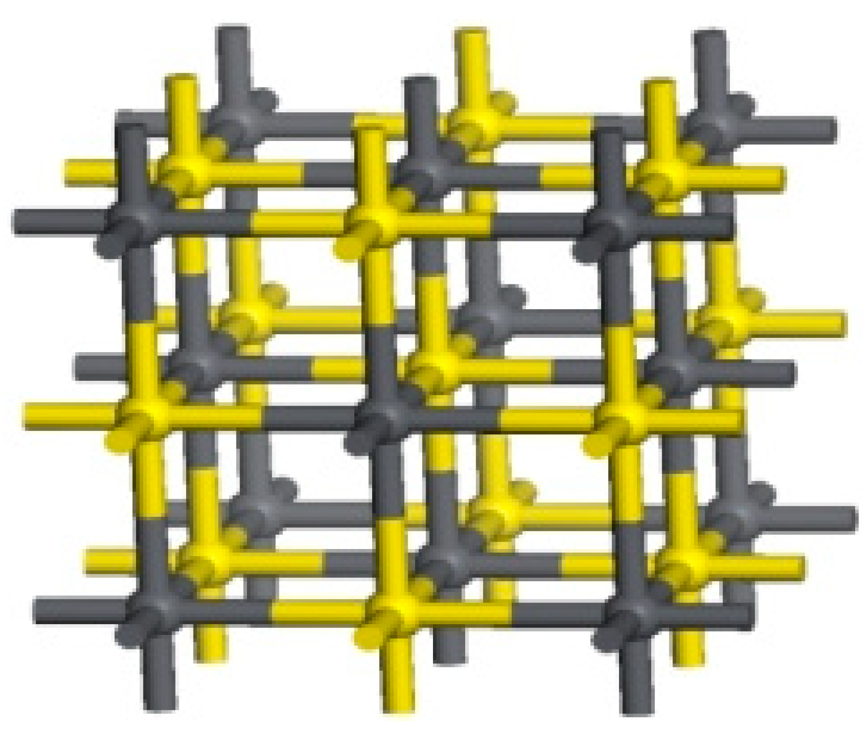
The ideal galena lattice model constructed according to known parameters is shown in Figure 1.
To make the lattice constant and the band gap of the model closer to the experimental value, it is necessary to optimize the original cell of galena and finally determine the best exchange-correlation functions and energy cut-off. In this study, the CASTEP module based on density functional in the Materials Studio software was employed for calculation. For the optimization process of the galena lattice system, researchers mainly adopt the following geometric optimization criteria: exchange-correlation functions and energy cut-off were GGA-PW91 and 300 eV, respectively. In addition, the convergence criteria of geometric optimization were set as follows: atomic displacement was 0.002 Å, interatomic force was 0.05 eV·Å, interatomic internal stress was 0.1 GPa, maximum energy change was 2.0 × 10⁻⁵ eV/atom; self-consistent iteration was 2.0 × 10⁻⁶ eV/atom; convergence accuracy of self-consistent iteration was 2.0 × 10⁻⁶ eV/atom; smearing value calculated by state density property was 0.1 eV. The valence electrons selected for the pseudopotential calculation of atoms are 5d106s26p2 of Pb and 3s23p4 of S [27,28].
The (100) surface of the galena was cut out from the optimized galena cell. A vacuum layer of 10 Å was added to eliminate the influence of periodic boundaries. The CASTEP module in the Materials Studio software was adopted to test the convergence of atomic layer numbers on galena surfaces based on first-principles density functional theory, which obtained a surface model consistent with practice. The exchange-correlation functions and the plane wave cut-off energy were selected from the convergence results of galena crystal cells.
The number of atomic layers was determined by studying the surface energy of galena with different atomic layers. When the number of atomic layers is different, the surface energy of the galena surface is calculated according to the following formula [29]:
E s u r f = E s l a b n E b u i k 2 A
E s u r f is the unit area of the surface energy, E s l a b represents the total free energy of the slab, n is the total number of atoms in the slab, E b u i k is the free energy of each atom inside the crystal, and A represents the unit area of the surface.

2.2. Crystal Structure Analysis of Galena

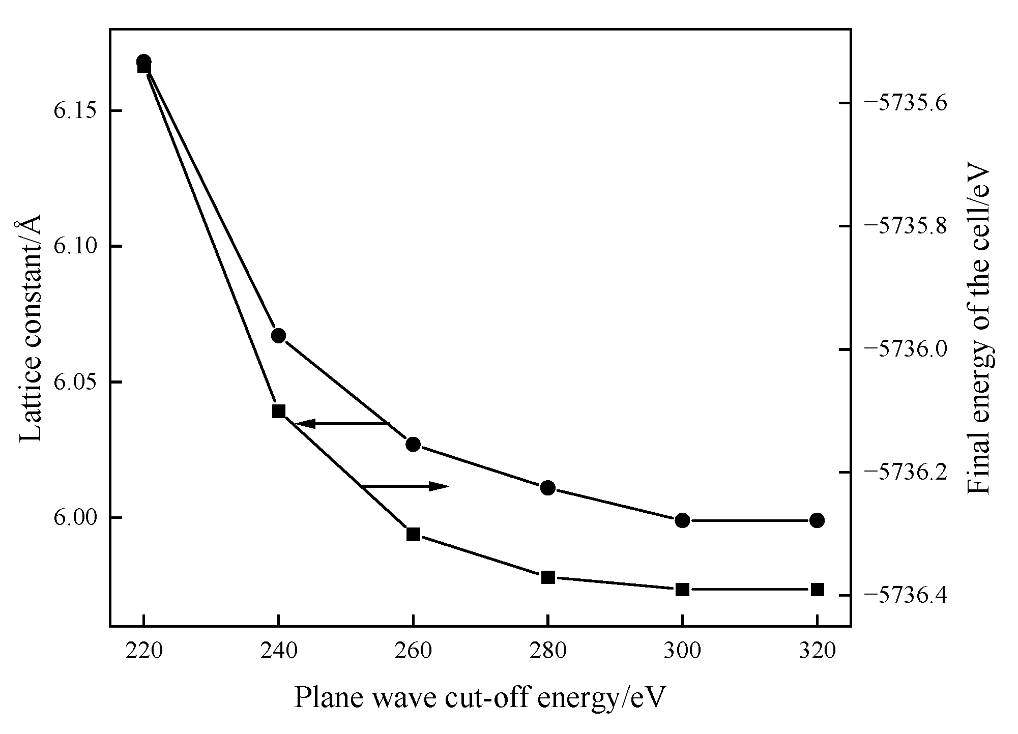
The lattice protocell model of galena is optimized by changing different plane wave cut-off energies and using existing optimization parameters. The cut-off energy with the minimum final energy of the cell is selected to determine the optimal cut-off energy of the plane wave in the optimization process. The software simulation results are shown in Figure 2.
As shown in Figure 2, the lattice constant and final energy of the cell decrease with the increase in the plane wave cut-off energy, reaching the lowest level when the cut-off energy was 300 eV. At this point, the lattice constant of 5.999 Å is closest to the experimental value of 5.9315 Å. The larger the plane wave cut-off energy is, the more accurate the lattice constants will be, but the amount of software calculation is also increasing. Therefore, the cut-off energy is selected as 300 eV.
The plane wave cut-off energy of 300 eV is selected, and the remaining parameters are unchanged to obtain the best exchange-correlation function. By changing different exchange-correlation functions and using software for simulation calculation, the best exchange-correlation function was determined in the optimization process of galena crystal. The simulation results are presented in Table 1.
As is evident from Table 1, the band gap of the exchange-correlation functions LDA-CA-PZ, GGA-RPBE, and GGA-WC groups have a significant large deviation from the experimental value of 0.41 eV. Although the final energy of the cell of the exchange-correlation function GGA-PBE is lower than GGA-PW91, the lattice constant and band gap width of GGA-PW91 are closer to the standard value. Therefore, the exchange-correlation function GGA-PW91 is selected comprehensively.
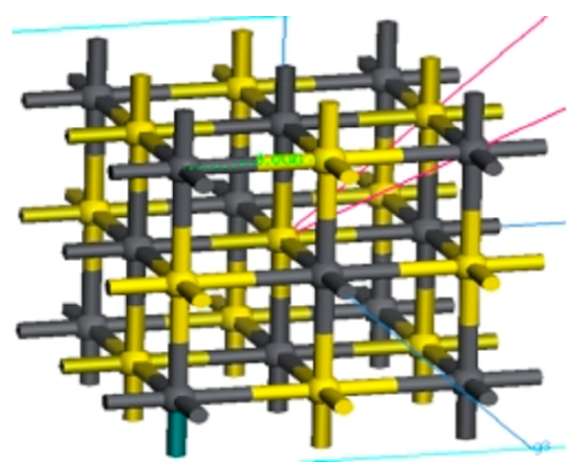
In the crystal structure of galena, the bond distance of Pb-S was 2.966 Å obtained from known lattice parameters, and the structure optimization was carried out. With the rest remaining unchanged, the exchange-correlation function and energy cut-off in the geometric optimization standard are GGA-PW91 and 300 eV, respectively. The bond distance of Pb-S in the crystal structure of galena after structural optimization was 3.000 Å as shown in Figure 3.
Table 2 compares the theoretical and experimental values of the lattice constant and band gap of galena under ideal conditions. It can be seen that the experimental lattice constant value of galena crystal is 0.5999 nm, which is very close to the theoretical value of 0.5931 nm. This shows that the model selected for the simulation and optimization of the galena lattice model is reasonable.
Chen et al. [30], using the Generalized gradient approximation (GGA) method to simulate the calculation of electronic structure properties of galena, examined the different exchange-correlation function effects on its lattice parameters (Table 3). The lattice parameters of galena: a = b = c = 5.9324 Å, α = β = γ = 90°.
As is evident from Table 1 and Table 3, the band gaps of the exchange-correlation functions GGA-RPBE and GGA-PBE both have a significantly large deviation from the experimental value of 0.41 eV. From the exchange functions of GGA-PW91 and GGA-WC, it is obvious that the results in this paper are more accurate than those of Chen et al. Therefore, our calculations are without spin-orbit coupling (SOC).
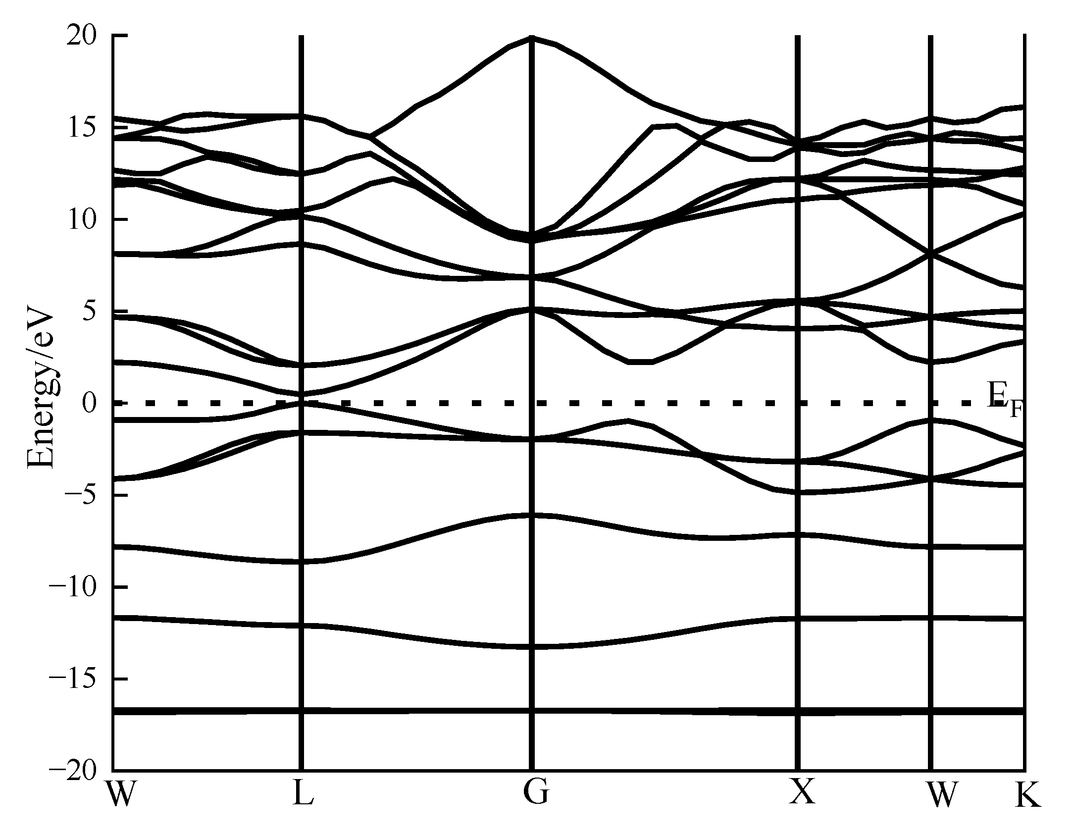
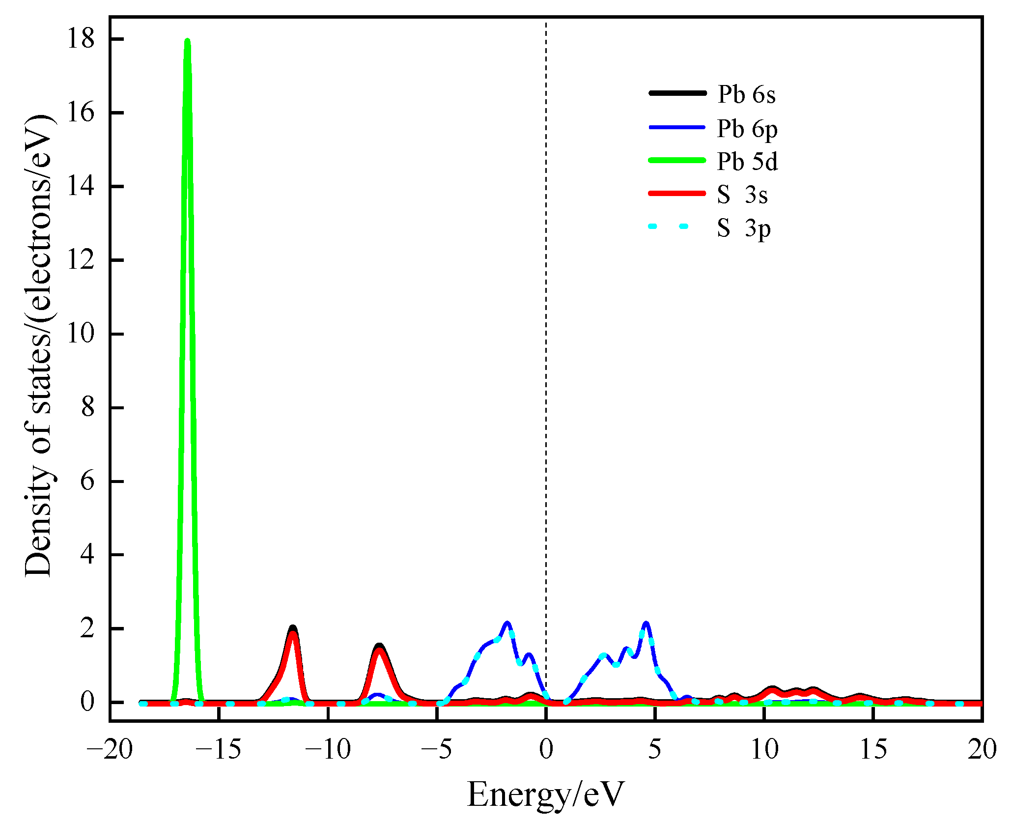
Figure 4 and Figure 5 show the band structure and density of states of perfect galena, calculated using CASTEP module simulation.
As demonstrated in Figure 4, the maximum value of the valence band and the minimum value of the conduction band in the band structure diagram of galena are both located at the highly symmetric G point, confirming that galena is a direct band-gap P-type semiconductor.
According to the density of states distribution diagram of galena in Figure 5, the upper valence band and the guide band are mainly composed of the 5d orbital of the Pb atom and the 3p orbital of the S atom. The lower valence band is comprised of the 5d orbital of the Pb atom.
Mulliken population distribution reflects the overlap of electrons between two atoms, providing a criterion for ionic and covalent bonding between them. The value of the Mulliken overlapping population indicates the degree of charge overlap between atoms, that is, the covalent strength of bonds between atoms. The results of the Mulliken population analysis of galena atoms are shown in Table 4.
As can be seen from Table 4, the valence electron configuration of the S atom is 3s23p4 before structural optimization, while the optimized valence electron configuration of the S atom is 3s1.923p4.73. The number of electrons localized in the S atom is 6.64 e, so the S atom obtains 0.64 e. Because its charge is −0.64e, it is an electron acceptor. It can be seen that the electrons are mainly obtained from the 3p orbital of the S. Before the structural optimization, the valence electron configuration of the Pb atom is Pb 5d10 6s2 6p2. In contrast, the optimized valence electron configuration of the Pb atom is Pb 5d106s3.926p1.44. The number of electrons localized in the Pb atom is 13.36, so the Pb atom decreases by 0.64e. Because its charge is +0.64 e, it is the electron donor. It is mostly losing electrons in the 6s and 6p orbitals of Pb. In addition, the 3p orbital of S and the 6p orbital of Pb contribute to the formation of PbS crystals from the data in the table.
Table 5 shows the atomic orbital coefficients composed of the highest occupied molecular orbital (HOMO) and the lowest unoccupied molecular orbital (LUMO) of galena electrons. The positive and negative signs of the coefficients represent the bonding and antibonding between atoms. The absolute values of the coefficients indicate the contribution to frontier orbits. Ordinarily, the most easily transferred orbit of electrons is the highest orbit occupied by electrons, while the most easily obtained orbit is the lowest unoccupied one. In short, the HOMO and LUMO orbitals are nucleophilic and electrophilic, respectively. According to the absolute value of the atomic coefficient in Table 5, it can be found that S atoms mainly contribute to the highest orbital. In contrast, Pb atoms contribute primarily to the lowest unoccupied orbital. Therefore, S atoms in galena are easy to lose electrons and undergo oxidation, while Pb atoms are easy to interact with anions.

2.3. Surface Structure and Electronic Properties of Galena

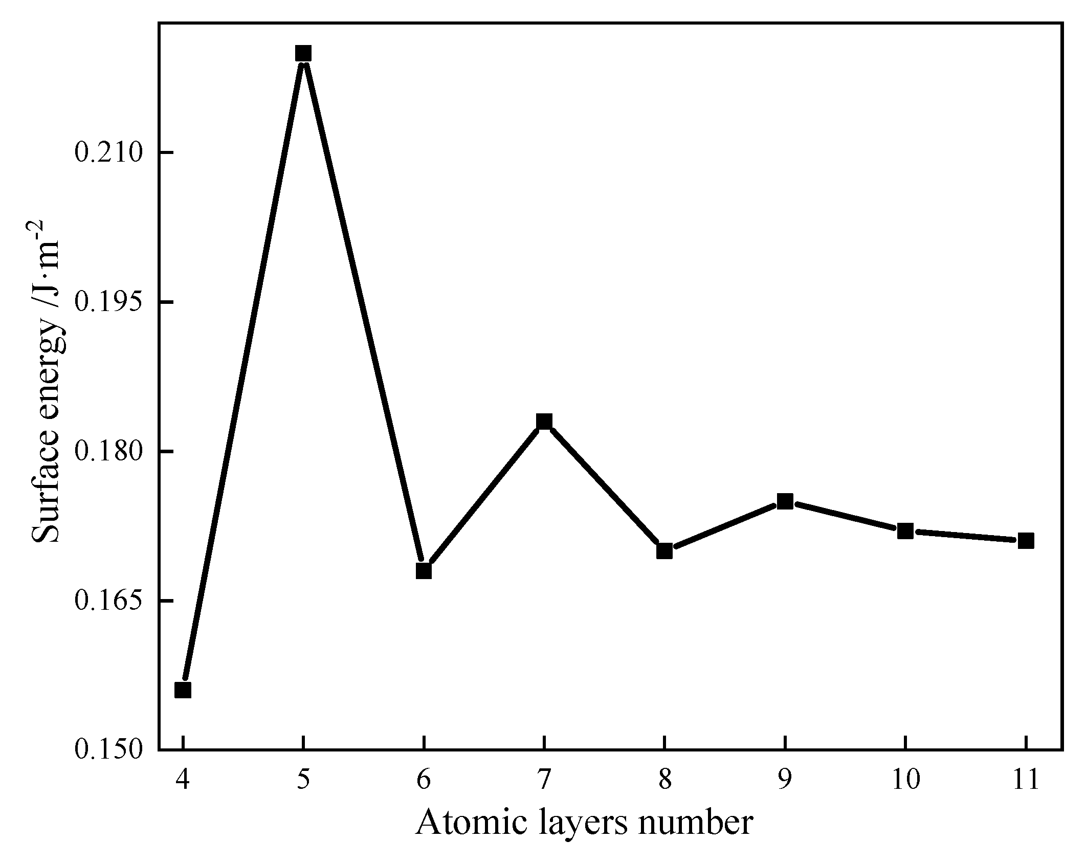
In this study, the relationship between atomic layers and surface energy was investigated using the surface of galena (100) of 431 super crystal cells. The results are indicated in Figure 6.
As demonstrated in Figure 6, when the atomic layer number is small, the variation range of the surface energy of galena decreases gradually with the increase in the atomic layer number. When the atomic layer number is 8, the surface energy change tends to be gentle. Therefore, the atomic layer number and thickness of the vacuum layer of the galena surface model are 8 and 15 Å, respectively.
The solid crystal structure is a stable periodic lattice structure. The mineral surface is exposed by breaking part of the connecting bonds, resulting in a structure different from the internal atomic environment. The force on such an aperiodic surface structure is no longer symmetrical. To achieve a new equilibrium, the phenomenon of readjusting the spacing of surface atoms is called surface relaxation [31].
The dissociation of the galena surface causes the atomic coordination number of Pb and S to decrease to five, which weakens the binding force of galena surface atoms, resulting in surface relaxation. Table 6 shows the displacement of the three layers of atoms on the galena surface before and after optimization.
As indicated in Table 6, the relaxation of Pb and S atoms in the three layers on the surface mainly occurs in the vertical direction, while the relaxation displacement in the horizontal direction is small. In general, the relaxation of the ideal (100) surface of the galena is minimal. There is no evident surface reconstruction, so during the surface optimization calculation, only the lower five layers of atoms need to be fixed to relax the three layers of atoms on the surface. At this time, the calculation can be reduced under the condition of ensuring accuracy. 
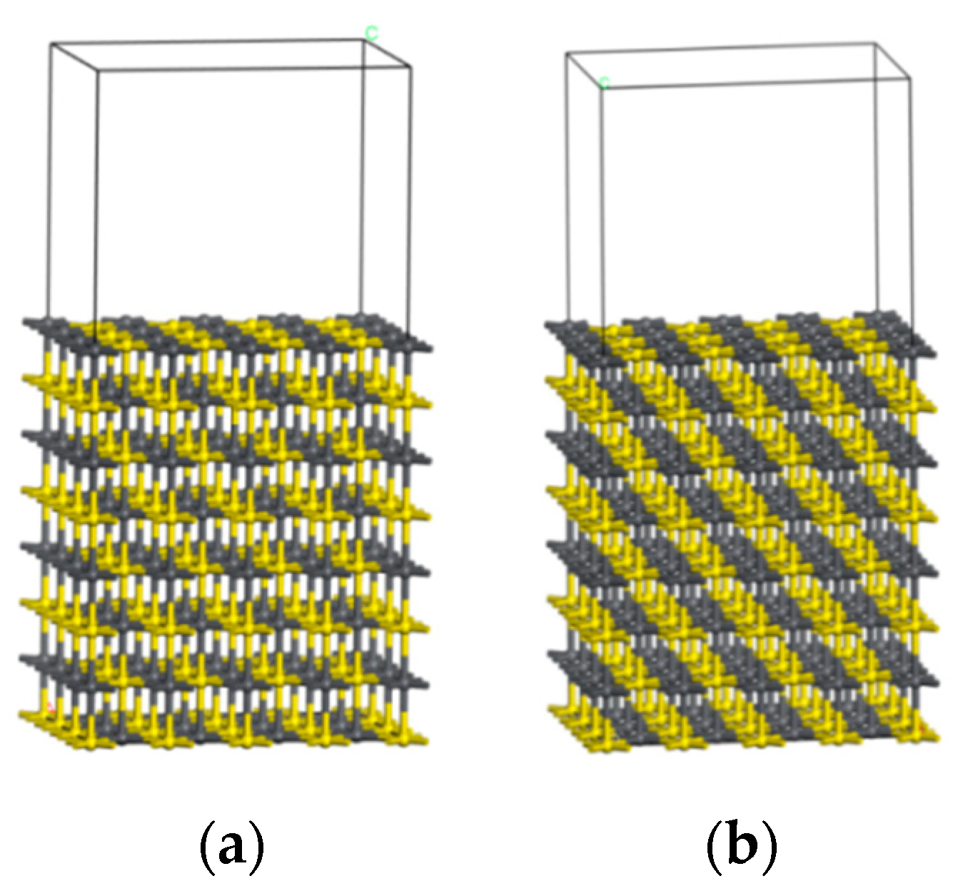
Figure 7 shows the crystal plane model before and after surface relaxation on the (100) cleavage surface of the galena.
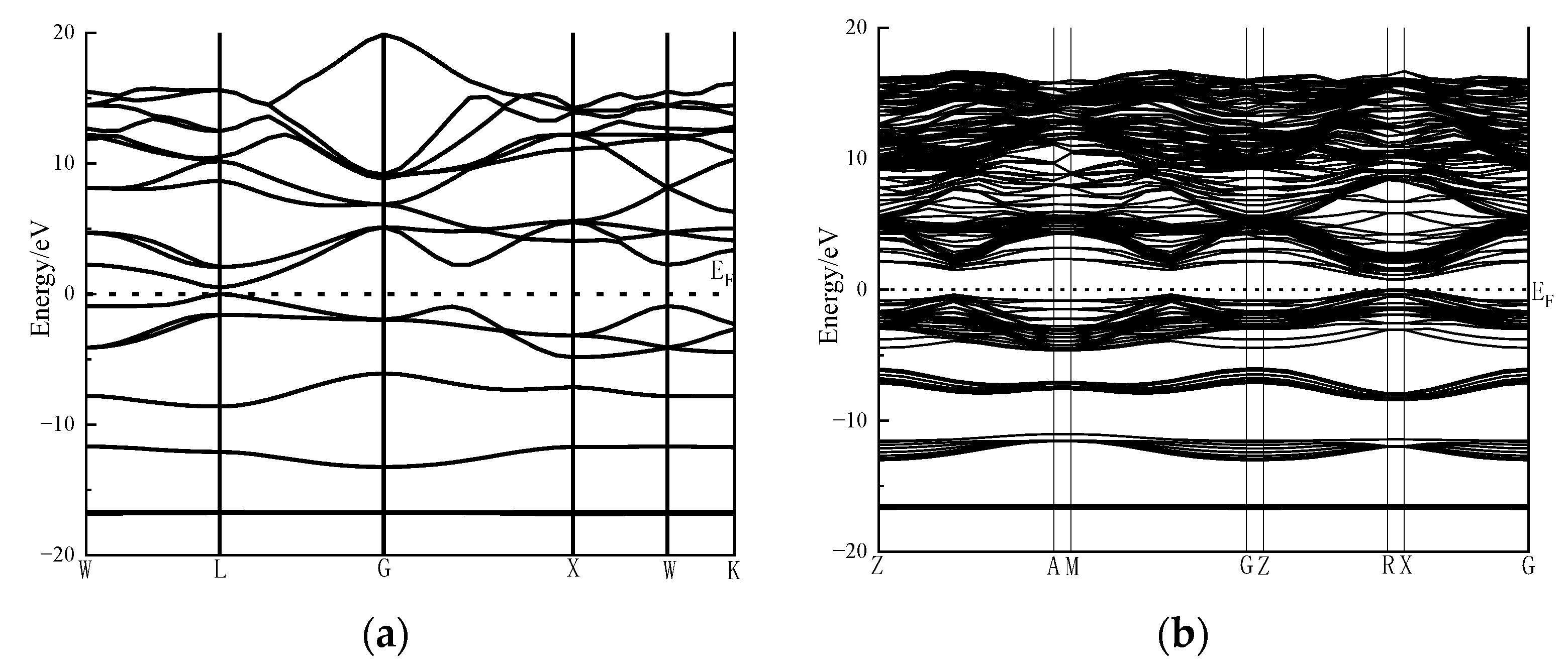
The environment of the atoms on the surface layer is different from that in the bulk, which is unsaturated and shows vigorous surface-reaction activity. The band gap is an essential characteristic parameter of semiconductors, and its size is related to the band structure of semiconductors. In other words, the band gap is associated with the crystal structure and atomic binding energy. The band structure of bulk galena (a) and (100) surface (b) are displayed in Figure 8.
As presented in Figure 8, when more atoms are used, the energy band curves of the galena surface model are denser than those of the bulk model. The simulation results show that the band gap of the galena bulk and the surface is 0.478 eV and 0.787 eV, respectively. The change in the band gap indicates that the electronic structure of the galena surface has changed significantly. Meanwhile, the electron transition from the valence band to the conduction band requires more energy.
According to previous research on the relaxation of galena surface structure, it was found that the galena surface undergoes significant relaxation. Therefore, it can be inferred that although the coordination number of atoms on the surface of galena is reduced compared to the bulk, the change of coordination number is weakened due to the large atomic number of Pb atoms and strong binding effect on valence electrons. The immense relaxation on the surface structure of galena has a marked impact on the binding of valence electrons, leading to an increase in electron transition energy. Therefore, the electronic activity of the galena surface is weakened.
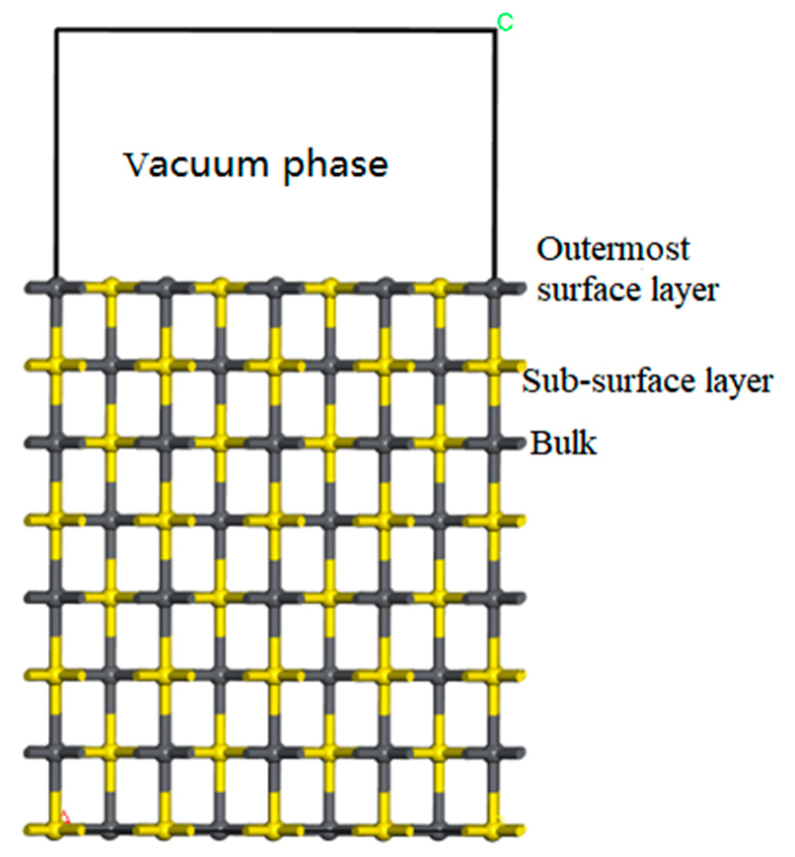
Figure 9 shows the outermost surface layer, sub-surface layer, and bulk on the surface (100) of the galena.
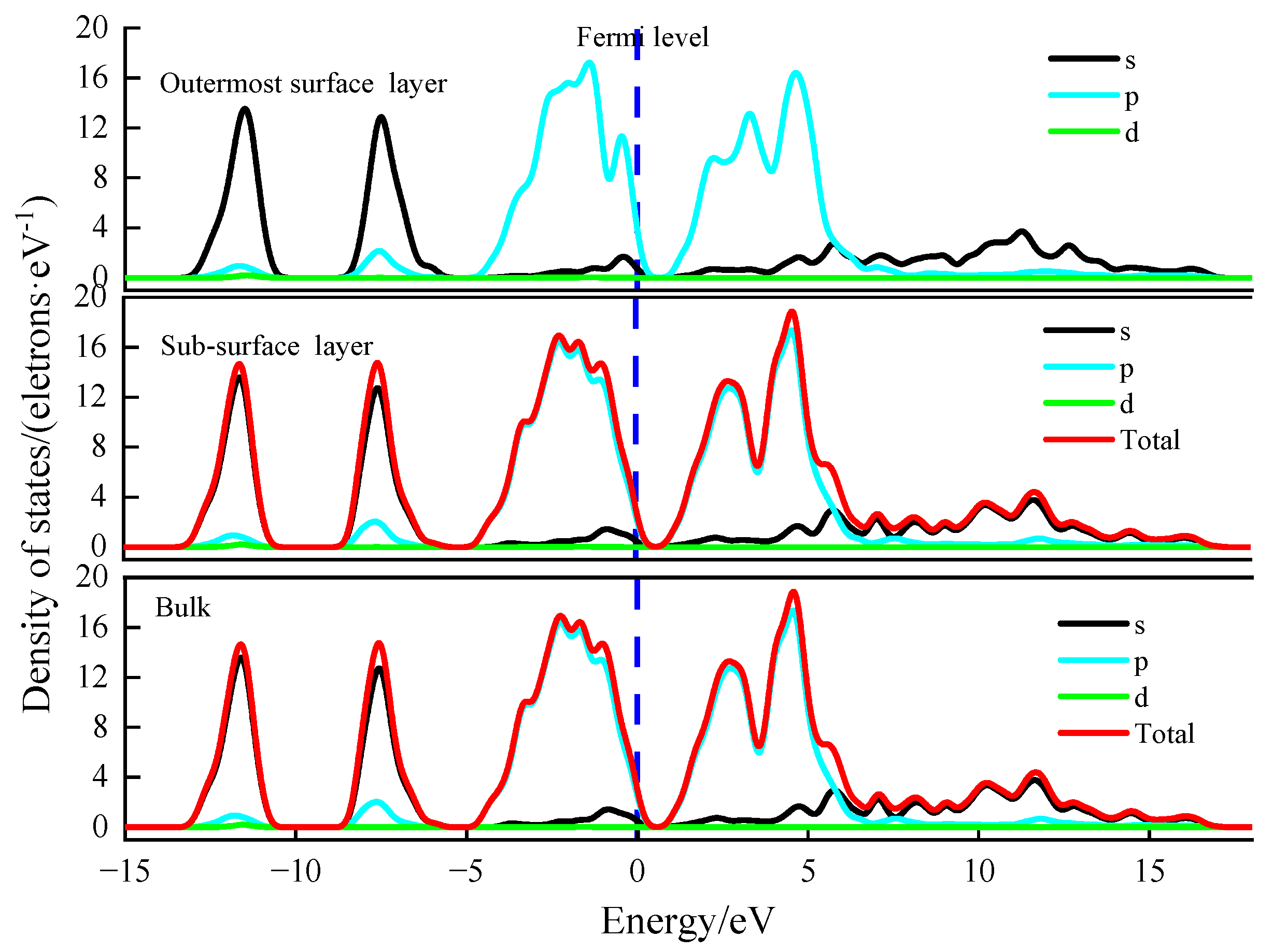
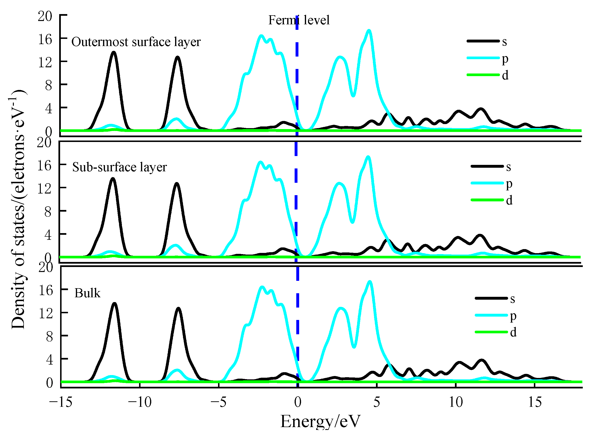
 Figure 10 and Figure 11 are acquired by calculating the state density with Pb atoms and S atoms in the outermost surface layer, sub-surface layer, and bulk.
As can be seen in Figure 10, the density of S atomic states in the outermost surface layer, sub-surface layer, and bulk on the (100) surface of galena are basically similar, which is consistent with the atomic relaxation results on galena surface.
It can be seen from the density of states of Pb atoms of the outermost surface layer, sub-surface layer, and bulk on (100) surface of galena in Figure 11 that the 6p density of states peak of the Pb and S atoms in these layers is the strongest at −2 eV, which shows that the Fermi level is mainly affected by the 6p orbital of Pb.
The positions of Pb and S atoms in each layer of the galena lattice are at the same height. In addition, the structure of their surface is relatively uncomplicated. Table 7 shows the electronic changes of the three layers of the galena surface after surface relaxation.
As presented in Table 7, the charge of the S atom changes from −0.71 e in the bulk to −0.61e in the outermost surface layer. In comparison, the charge of the Pb atom decreases from 0.7e in the bulk to 0.67 e in the sub-surface layer and then to 0.61 e in the outermost surface layer. From the perspective of electron orbital distribution, the valence electron structure adopted in the calculation is 5d106s26p2 for the Pb atom and 3s23p4 for the S atom. The analysis found that the 3p orbital of S and the 6p orbital of Pb mainly play a role in galena crystal. Ordinarily, electrons from the 6p orbital of Pb will transfer to the 3p orbital of S, resulting in the change of atomic valence states on the lattice surface. It can also be seen from Table 6 that, in the process of relaxation of the galena surface structure, electrons change from 4.74 in the bulk to 4.75 in the outermost surface layer in the 3p orbital of S, and electrons are both 1.41 in the bulk and outermost surface layer in 6p orbital of Pb. These indicate that the role of the 3p orbital of S and 6p orbital of Pb will not be affected in this process. However, the electrons in the 6s orbital of Pb in the outermost surface layer change from 6s1.88 in the bulk to 6s1.98 on the outermost surface layer surface. According to the electron distribution and charge change on the galena surface, the total electron number of the outermost surface layer was higher than that of the bulk, so the galena surface owns the properties of electron enrichment.

3. Conclusions

During the formation of the galena crystal, the 3p orbital of S and the 6p orbital of Pb played a primary role. Therefore, S atoms in galena easily lose electrons and are oxidized, while Pb readily reacts with anions. The change in coordination number is weakened due to the large atomic number of Pb atoms and the strong binding effect on valence electrons. The significant relaxation on the surface structure of galena has a marked impact on the binding of valence electrons, leading to the increase in electron transition energy. Ordinarily, electrons from the 6p orbital of Pb will transfer to the 3p orbital of S, resulting in the change of atomic valence states on the lattice surface. According to the electron distribution and charge change on the galena surface, the total electron number of the outermost surface layer was higher than that of the bulk. Therefore, the galena surface possesses the properties of electron enrichment.

Author Contributions

Conceptualization, J.K.; methodology, X.M. and F.C.; software, F.C.; validation, J.X. and S.W.; formal analysis, H.W. and J.L.; investigation, X.M. and C.Z.; resources, C.Z. and X.B.; data curation, J.K. and J.L.; writing—original draft preparation, Y.A. and H.W.; writing—review and editing, Y.A.; supervision, J.K. and S.W.; project administration, X.B.; funding acquisition, X.B. and J.X. All authors have read and agreed to the published version of the manuscript.

Funding

The authors are grateful for the financial support from the National Natural Science Foundation of China (No. 52074206), the Key Research and Development Project of Anhui Province (202104a07020012), the Natural Science Basic Research Plan in Shaanxi Province of China (No. 2021JQ-507), the Special Research Project of Shaanxi Education Department, China (No. 21JK0731), and the Talent Science and Technology Fund of Xi’an University of Architecture and Technology, China (No. ZR20066).

Institutional Review Board Statement

Not applicable.

Informed Consent Statement

Not applicable.

Data Availability Statement

Not applicable.

Conflicts of Interest

The authors declare no conflict of interest.

References

  1. Wen, H.R.; Li, L.J. Experimental study on preferential flotation of a mixed lead-zinc deposit in Sichuan. Min. Res. Dev. 2021, 41, 121–126. [Google Scholar]
  2. Gu, J.N.; Zhang, X.Y.; Han, J.X.; Zhao, Z.Z. Global lead resources situation and the development of leadership resources in China. China Min. Mag. 2017, 26, 16–20. [Google Scholar]
  3. Chen, X.F.; Peng, R.M. Pb-Zn metal resources condition and strategy for Pb-Zn metals industry sustainable development in China. Nonferrous Met. 2008, 60, 129–132. [Google Scholar]
  4. Su, C.; Liu, D.W.; Shen, P.L.; Cai, J.P.; Yang, S.W.; Li, J.L. Research progress in electrochemical characteristics and flotation behavior of chalcopyrite and galena. Nonferrous Met. Eng. 2020, 10, 79–87. [Google Scholar]
  5. Zhang, Y.; Liu, R.Q.; Sun, W.; Wang, L.; Dong, Y.H.; Wang, C.T. Electrochemical mechanism and flotation of chalcopyrite and galena in the presence of sodium silicate and so dium sulfite. Trans. Nonferrous Met. Soc. China 2020, 30, 1091–1101. [Google Scholar] [CrossRef]
  6. Zhou, W.T.; Han, Y.X.; Sun, Y.S.; Yang, J.L.; Ma, S.J. Multi-scale impact crushing characteristics of polymetallic sulfide ores. Trans. Nonferrous Met. Soc. China 2019, 29, 1929–1938. [Google Scholar] [CrossRef]
  7. Wei, M.A.; Sun, C.Y. Review and development tendency of the Copper and Lead sulfides flotation separations. Min. Metall. 2008, 2, 6–16. [Google Scholar]
  8. Zhang, Q.; Feng, Q.C.; Wen, S.M.; Liu, J.B. Bulk flotation of highly oxidized Cu-Pb-Zn ore at Jiama Tibet. J. Kunming Univ. Sci. Technol. 2019, 44, 32–39. [Google Scholar]
  9. Xu, F.F. Study on flotation test for copper-lead-zinc polymetallic sulfide ore of Henan. Nonferrous Met. 2019, 4, 52–57. [Google Scholar]
  10. Zhao, K.L.; Gu, G.H.; Ma, C. Study on the mechanism of nontoxic depressant in copper-lead flotation separation and its application. Nonferrous Met. 2021, 3, 56–61. [Google Scholar]
  11. Kang, B.W.; Xie, X.; Chen, G.Q.; Fan, P.Q.; Song, Q. Translation Research status and progress of lead inhibitors in the online copper sulfide lead mineral separation process. Met. Min. 2018, 10, 104–109. [Google Scholar]
  12. Wang, P.; Cheng, X.X.; Zhang, H.; Dai, T.P. Experimental research on the separation of multiple metals in one gold ore from Inner Mongolia containing copper, lead, and zinc. Gold 2019, 37, 49–53. [Google Scholar]
  13. Li, J. Study on mineral processing of copper-lead-zinc ore in Tibet. Gansu Metall. 2010, 32, 50–53. [Google Scholar]
  14. Sun, G.Z.; Chen, Y.; Li, X.Y.; Wang, D.Y. Experimental research on flotation separation of refractory copper-lead sulfide ore in Yunnan province. Nonferrous Met. 2017, 5, 9–13. [Google Scholar]
  15. Chen, J.H.; Long, X.H.; Zhao, C.H.; Kang, D.; Guo, J. DFT calculation on relaxation and electronic structure of sulfide minerals surfaces in presence of H2O molecule. J. Cent. South Univ. 2014, 21, 3945–3954. [Google Scholar] [CrossRef]
  16. Wang, D.Z.; Long, X.Y.; Sun, S.Y. Quantum chemistry study on oxidation of sulfide minerals and their flotation mechanism. Trans. Nonferrous Met. Soc. China 1991, 1, 15–23. [Google Scholar]
  17. Yang, G.; Long, X.Y. A quantum chemistry study on the electronic structure of mercapto flotation reagents and its coordination with metal ions. Chem. J. Chin. Univ. 2001, 22, 86–90. [Google Scholar]
  18. Ding, D.H.; Long, X.Y.; Wang, D.Z. Mechanism of pyrite oxidation and flotation. Nonferrous Met. 1993, 45, 24–30. [Google Scholar]
  19. Long, X.Y.; Wang, F.Z.; Wang, D.Z. Electronic structure of galena surface oxidation and flotation mechanism. Nonferrous Met. 1992, 44, 42–47. [Google Scholar]
  20. Li, Y.B.; Wei, Z.L.; Xiao, Q.; Gao, H.M.; Song, S.X. A fundamental DFT study of chalcopyrite surface evolution due to impurity divalent ions during the leaching process. Miner. Eng. 2018, 121, 205–211. [Google Scholar] [CrossRef]
  21. Ke, B.L.; Li, Y.Q.; Chen, J.H.; Zhao, C.H.; Chen, Y. DFT study on the galvanic interaction between pyrite (100) and galena (100) surfaces. Appl. Surf. Sci. 2016, 367, 270–276. [Google Scholar] [CrossRef]
  22. Long, X.H.; Chen, Y.; Chen, J.H.; Xu, Z.H.; Liu, Q.X.; Du, Z. The effect of water molecules on the thiol collector interaction on the galena (PbS) and sphalerite (ZnS) surfaces: A DFT study. Appl. Surf. Sci. 2016, 389, 103–111. [Google Scholar] [CrossRef]
  23. Chen, J.H.; Ke, B.L.; Lan, L.H.; Li, Y.Q. DFT and experimental studies of oxygen adsorption on galena surface bearing Ag, Mn, Bi, and Cu impurities. Miner. Eng. 2015, 71, 170–179. [Google Scholar]
  24. Chen, J.H.; Wang, L.; Chen, Y.; Guo, J. A DFT study of the effect of natural impurities on the electronic structure of galena. Int. J. Miner. Process. 2010, 98, 132–136. [Google Scholar] [CrossRef]
  25. Chen, J.H.; Long, X.H.; Chen, Y. Comparison of Multilayer Water Adsorption on the Hydrophobic Galena (PbS) and Hydrophilic Pyrite (FeS2) Surfaces: A DFT Study. J. Phys. Chem. C 2014, 118, 11657–11665. [Google Scholar] [CrossRef]
  26. Li, Y.Q.; Chen, J.H.; Chen, Y.; Zhu, Y.G.; Liu, Y.C. DFT Simulation on Interaction of H2O Molecules with ZnS and Cu-Activated Surfaces. J. Phys. Chem. C 2019, 123, 3048–3057. [Google Scholar] [CrossRef]
  27. Lan, L.H.; Chen, J.H.; Li, Y.Q.; Lan, P.; Yang, Z.; Ai, G.H. Microthermokinetic study of xanthate adsorption on impurity-doped galena. Trans. Nonferrous Met. Soc. China 2016, 26, 272–281. [Google Scholar] [CrossRef]
  28. Duan, Y.F.; Tang, G.; Chen, C.Q.; Lu, T.J.; Wu, Z.G. First-principles investigations of ferroelectricity and piezoelectricity in BaTiO3/PbTiO3 superlattices. Phys. Rev. B 2012, 85, 054108. [Google Scholar] [CrossRef]
  29. Xie, R.Q.; Zhu, Y.M.; Liu, J.; Li, Y.J. The first principle calculation of spodumene electronic structure and surface chemistry features of spodumene (110) surface. Met. Mine 2020, 6, 68–74. [Google Scholar]
  30. Chen, J.L.; Wang, L.; Chen, Y.; Li, Y.Q.; Guo, J. Density functional theory of effects of vacancy defects onelectronic structure and flotation of galena. Chin. J. Nonferrous Met. 2012, 20, 1815–1821. [Google Scholar]
  31. Lan, L.H.; Ai, G.Y.; Wang, J.Q.; Lan, P.; Chen, J.H. First-principles calculation of electronic structure and optical properties of galena with doping. Sci. Technol. Eng. 2017, 17, 152–155. [Google Scholar]
Figure 1. Crystal structure of perfect galena (Yellow: S atoms; Gray: Pb atoms).
Processes 11 00619 g001
Figure 2. Lattice constant and final energy of the cell of galena as a function of plane wave cut-off energy.
Processes 11 00619 g002
Figure 3. Optimized crystal structure of perfect galena (Yellow: S atoms; Gray: Pb atoms).
Processes 11 00619 g003
Figure 4. Band structure of perfect galena.
Processes 11 00619 g004
Figure 5. The density of states of perfect galena.
Processes 11 00619 g005
Figure 6. Relation of atomic layer number and surface energy of galena.
Processes 11 00619 g006
Figure 7. Crystal plane model before and after surface relaxation on (100) cleavage surface of galena (Yellow: S atoms; Gray: Pb atoms). (a) Before surface relaxation; (b) After surface relaxation.
Processes 11 00619 g007
Figure 8. Band structure of bulk galena (a) and (100) surface (b).
Processes 11 00619 g008
Figure 9. Outermost surface layer, sub-surface layer, and bulk on (100) surface of galena (Yellow: S atom; Gray: Pb atoms).
Processes 11 00619 g009
Figure 10. The density state of S atoms of the outermost surface layer, sub-surface layer, and bulk on (100) surface of the galena.
Processes 11 00619 g010
Figure 11. The density state of Pb atoms of the outermost surface layer, sub-surface layer, and bulk on (100) surface of the galena.
Processes 11 00619 g011
Table 1. The optimized result using different exchange-correlation functions.
Exchange-Correlation FunctionsLattice Constant (Å)Band Gap (eV)Final Energy of Cell (eV)
LDA-CA-PZ5.84360.066−5737.17
GGA-PBE6.00530.496−5734.13
GGA-RPBE6.08130.716−5733.70
GGA-PW915.99990.478−5736.39
GGA-WC5.90210.196−5734.31
Table 2. Lattice constant and band gap of perfect galena.
ParameterTheoretical ValueExperimental Value
Lattice constant0.5931 nm0.5999 nm
band gap0.41 eV0.478 eV
Table 3. Optimized results by different exchange-correlation functions.
FunctionsCell Constant (Å)Band Gap (eV)
GGA-PBE6.02400.546
GGA-RPBE6.08680.756
GGA-PW916.03800.527
GGA-WC5.93020.230
Table 4. Mulliken atomic population analysis of galena.
AtomspdfTotal ChargeCharge Change (e)
S1.924.730.000.006.64−0.64
Pb1.921.4410.000.0013.360.64
Table 5. Frontier orbital and atom orbital coefficients of galena.
Mineral Crystal Frontier OrbitalAtom Orbital Coefficient
GalenaHOMO−0.493 S(3p − 1) + 0.038 Pb(6p − 1)
LUMO0.484 Pb(6p − 1) + 0.203 S(3p − 1)
Table 6. The displacement of the three layers of atoms on the galena surface before and after optimization.
LayerAtomicCoordination NumberAtomic Displacement (nm)
∆x (nm)∆y (nm)∆z (nm)
Outermost surface layerPb5−0.0001−0.0001−0.0082
S500−0.0101
Sub-surface layerPb6000.0102
S60.0001−0.00030.0128
BulkPb6−0.0001−0.0001−0.0040
S600−0.0060
Table 7. Mulliken charge of galena (100) surface after relaxation.
Layer Atoms (e)p (e)d (e)Total Charge (e)Charge Change (e)
Outermost surface layerPb1.981.4110.0013.390.61
S1.934.750.006.68−0.61
Sub-surface layerPb1.901.4310.0013.330.67
S1.924.730.006.65−0.67
BulkPb1.881.4110.0013.290.71
S1.934.740.006.67−0.71
Disclaimer/Publisher’s Note: The statements, opinions and data contained in all publications are solely those of the individual author(s) and contributor(s) and not of MDPI and/or the editor(s). MDPI and/or the editor(s) disclaim responsibility for any injury to people or property resulting from any ideas, methods, instructions or products referred to in the content.

