Article

High Efficiency and High Voltage Conversion Ratio Bidirectional Isolated DC–DC Converter for Energy Storage Systems

Department of Electronic Engineering, National Kaohsiung University of Science and Technology, Kaohsiung City 805301, Taiwan
*
Author to whom correspondence should be addressed.
Processes 2022, 10(12), 2711; https://doi.org/10.3390/pr10122711
Submission received: 11 November 2022 / Revised: 9 December 2022 / Accepted: 12 December 2022 / Published: 15 December 2022
(This article belongs to the Section Process Control and Monitoring)

Abstract

:
In this paper, a novel high-efficiency bidirectional isolated DC–DC converter that can be applied to an energy storage system for battery charging and discharging is proposed. By integrating a coupled inductor and switched-capacitor voltage doubler, the proposed converter can achieve isolation and bidirectional power flow. The proposed topology comprises five switches and a common core coupled inductor that uses only a set of complementary pulse-width-modulated signals to control and achieve high voltage gain without requiring high turn ratios or excessive duty cycles. Moreover, the proposed topology can recover the leakage inductance energy to improve the conversion efficiency. The main switches exhibit zero-voltage switching, which reduces the switching losses. A 500-W bidirectional converter is used to verify the feasibility of the proposed bidirectional converter through theoretical analysis and experiments. The experimental results indicate that the highest efficiency of the proposed converter in the step-up and step-down modes is 97.59% and 96.5%, respectively.

1. Introduction

Since the industrial revolution, fossil fuels have been used for generating power. The resulting emissions have caused serious damage to the environment. Therefore, countries worldwide have realized the importance of renewable energy and advocate for renewable energy generation systems [1]. However, renewable energy generation varies with changes in the weather and environment. To overcome this problem, an energy storage system is required. When excess renewable energy is produced, the excess electrical energy can be stored in an energy storage system. This energy can then be used when the electricity demand peaks. A distributed generation system [2,3] is required to support a renewable energy system, as shown in Figure 1.
In an energy storage system, a DC–DC converter is required to transfer energy between a battery and a DC bus. DC–DC converters are of two main types: isolated converters and nonisolated converters. Common nonisolated bidirectional converters are derived from the boost converter, buck-boost converter, single-ended primary-inductor converter, and other unidirectional converters that exhibit advantages such as low cost, high stability, and high practicability. However, nonisolated bidirectional converters are limited by their duty cycle and low voltage conversion ratio. Therefore, switched-capacitor [4,5,6], coupled-inductor [7], and cascaded [8,9,10] converters are used to improve the voltage gain.
Existing isolated bidirectional converters are mostly derived from forward-flyback converters [11,12] and bridge converters [13,14,15]. Isolated bidirectional converters exhibit advantages such as high stability and practicability; however, their circuit design is more complicated than that of nonisolated bidirectional converters. Rapid advancements have been made in bidirectional DC–DC converter technology. In recent years, studies have focused on increasing the conversion efficiency and reducing the number of components to improve the stability of converters.
A bidirectional buck-boost converter is a common topology that is mostly used in battery chargers [16,17,18,19]. A study proposed a nonisolated bidirectional quasi-Z-source DC–DC converter with high voltage gain; however, this converter does not have soft-switching technology and thus has a low conversion efficiency [20]. Another study developed a nonisolated interleaved converter with a three-phase interleaved switched-capacitor topology. This converter has advantages such as a high voltage gain and high power transmission; however, phase-shift control technology is required to control the aforementioned converter [21]. Coupled inductors have been incorporated into DC–DC nonisolated converters to increase the voltage gain of these converters [22,23,24]. Switches with zero-voltage switching (ZVS) can increase the conversion efficiency; however, a higher number of circuit components increases the cost of a converter [22,24]. Switches without ZVS require fewer components but exhibit higher losses than do those with ZVS [23]. A bidirectional forward-flyback converter with a simple circuit and low current ripple but a low voltage gain and complex control method was proposed in [25]. An isolated interleaved DC–DC converter with an interleaved topology that includes a voltage doubler (used to achieve high voltage gain and ZVS to increase efficiency) has been developed to reduce the current ripple; however, the circuit of this converter requires a complex control method and many components [26]. DC–DC converters with a wide input voltage range and high voltage gain have been developed [27,28]. One study used an additional active clamp to recycle the leakage inductor energy to increase the number of components and decrease the converter efficiency [27]. Another study used a current-fed topology to increase the output current of the low-voltage side of a converter to make this side suitable for battery charging; however, high current flows through the components of this converter, which results in it exhibiting high losses [28]. In contrast to the conventional dual-active-bridge converter, the bidirectional isolated bridge converter has been combined with a push–pull converter and full-bridge converter to reduce the number of switches required and thus the switching losses; however, the control method of the bidirectional isolated bridge converter is complex [29]. Another study used a three-winding coupled inductor and a half-wave voltage doubler to increase the voltage gain and lower the components of the circuit; however, the turns ratio of coupled inductor is high, which causes larger volume of the circuit [30]. In the present paper, a novel high-efficiency isolated DC–DC converter is proposed for an energy storage system. This converter can transfer energy between a battery and a DC bus. Since the common voltages of batteries and DC buses are 48 and 400 V, respectively, the low and high side voltages of the proposed converter are 48 and 400 V, respectively.

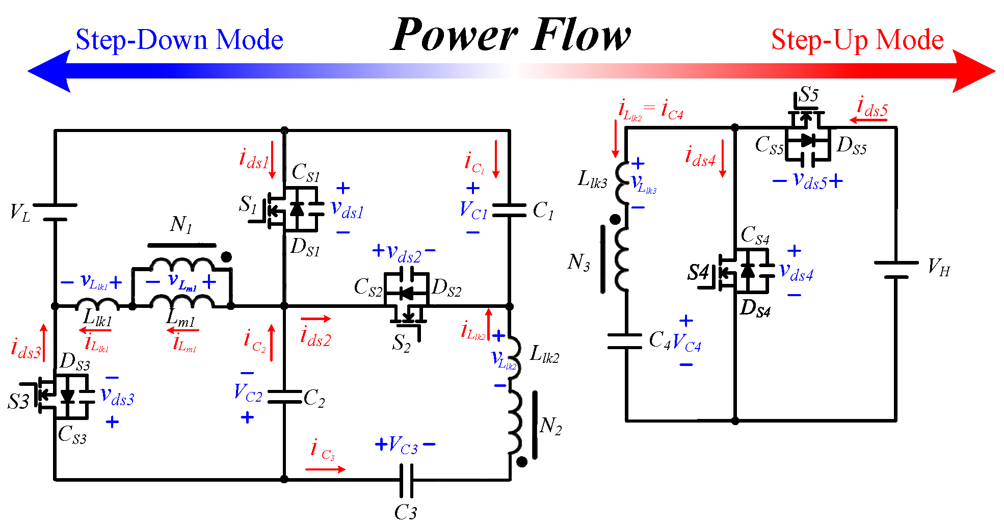
2. Circuit Architecture and Operation Principle

Figure 2 displays the circuit architecture of the proposed bidirectional converter. In this figure, VH and VL denote the high-voltage-side and low-voltage-side power ports, respectively. The coupled inductor consists of the leakage inductances Llk1, Llk2, and Llk3 as well as the magnetizing inductance Lm1. Moreover, the turn ratio of the inductor is represented by n. The proposed converter contains five switches (S1S5). The body diodes DS1DS5 and parasitic capacitances CS1CS5 are the parasitic elements of S1S5, respectively. The proposed converter also contains the capacitors C1C4. The operating principles and operation mode of the proposed topology in the step-up and step-down modes are analyzed.
This section discusses the operating principles of the proposed topology in the step-up and step-down modes. The voltage polarity and current direction of the components in the proposed topology are illustrated in Figure 2. To simplify our analysis of the operating principles, the following assumptions were made:
(1)
The internal resistance and parasitic effects can be ignored.
(2)
The voltages of the capacitors and currents of the inductors increase and decrease linearly.
(3)
The capacitances of C1, C2, C3, and C4 are infinite.
(4)
All the magnetic components operate in the continuous-current mode (CCM).
(5)
The number of turns N1 = N2 < N3, and N2/N1 = N3/N1 = n.

2.1. Step-Up Mode

In the step-up mode, the complementary pulse-width-modulated (PWM) signal comprises two sets of signals: (i) vgs1 and (ii) vgs2,3. The gate signal of S1 is the complementary waveform of S2 and S3. The signals of S4 and S5 are in the OFF state. The theoretical waveforms of the proposed topology in the step-up mode are displayed in Figure 3, and one operating cycle features five operation modes as shown in Figure 4a–e.
(1)
Mode 1 [t0–t1]
The equivalent circuit for the Mode 1 operation in the step-up mode is displayed in Figure 4a. This mode is operated in a dead-time period, and all switch signals are in the OFF state in Mode 1. At the beginning of this mode at time t = t0, the low-voltage side VL and leakage inductance Llk1 charge the capacitors C1 and C2. Mode 1 operation is followed by Mode 5 operation. To achieve ZVS, the energy of the parasitic capacitance of S1 is released through Llk2, and the energy of Llk2 is recycled by C1 and C2. The energy of the magnetizing inductance Lm1 and C3 is transferred to the high-voltage-side capacitor C4 through the coupled inductor, and Llk3 releases energy to C4. Mode 1 ends when S1 is turned on.
(2)
Mode 2 [t1–t2]
The equivalent circuit for Mode 2 operation is illustrated in Figure 4b. When S1 is completely turned on at time t = t1, the low-voltage side VL supplies energy to the magnetizing inductance Lm1 and leakage inductance Llk1. Moreover, a part of the energy of VL is transferred to the high-voltage side VH through the coupled inductor. The capacitors C1 and C2 release energy to C3 and the leakage inductance Llk2, and a part of this energy is transferred to VH through the coupled inductor. The capacitor C4 releases energy to Llk3 and VH.
(3)
Mode 3 [t2–t3]
The equivalent circuit for Mode 3 operation is depicted in Figure 4c. This mode is operated in a dead-time period, and all switch signals are in the OFF state in Mode 3. To achieve ZVS, the energy of the S3 parasitic capacitance is absorbed into the leakage inductance Llk1, and the energy of the S2 parasitic capacitance is absorbed into the leakage inductance Llk2. The energy of Llk1 is released to C1 and C2, and the energy of Llk2 is released to C2 and C3. The capacitor C4 and leakage inductance Llk3 release energy to VH. Mode 3 ends when S2 and S3 are completely turned on.
(4)
Mode 4 [t3–t4]
The equivalent circuit for Mode 4 operation is displayed in Figure 4d. When S2 and S3 are completely turned on at time t = t3, the leakage inductance Llk1 continuously releases energy to C1 and C2. Capacitor C3 charges C2 and Llk2. Moreover, a part of the energy of C3 is transferred to C4 and Llk3 through the coupled inductor. The magnetizing inductance Lm1 charges C4 and Llk3. Mode 4 ends when the capacitor voltage of C2 is higher than the voltage of N1.
(5)
Mode 5 [t4–t5]
The equivalent circuit for Mode 5 operation is illustrated in Figure 4e. At time t = t4, the switch signals are the same as those in Mode 4. In Mode 5, Llk1 releases energy to C1, and C3 charges C1, C2, and Llk2. Moreover, a part of the aforementioned energy is transferred through the coupled inductor to C4 and Llk3. Mode 5 ends when the current of Llk1 decreases to 0.

2.2. Step-Down Mode

In the step-down mode, the complementary PWM signal comprises two sets of signals: (1) vgs1,5 and (2) vgs2,3,4. The gate signals of S1 and S5 are complementary waveforms of those of S2, S3, and S4. The theoretical waveforms of the proposed topology in the step-down mode are shown in Figure 5, and one operating cycle contains seven operation modes Figure 6a–g.
(1)
Mode 1 [t0–t1]
The equivalent circuit for Mode 1 operation in the step-down mode is illustrated in Figure 6a. This mode is operated in a dead-time period, and all switch signals are in the OFF state. To achieve ZVS, the energy of the parasitic capacitance S5 is absorbed into the leakage inductance Llk3. Moreover, C1 and the magnetizing inductance Lm1 charge the low-voltage side VL, Llk1, and C3. Mode 1 is followed by Mode 5. C2 and Llk2 release energy to C3, and Mode 1 ends when S1 and S5 are completely turned on.
(2)
Mode 2 [t1–t2]
The equivalent circuit for Mode 2 operation is displayed in Figure 6b. When S1 and S5 are completely turned on at time t = t1, C1, C2, and Llk2 charge C3 continuously. The magnetizing inductance Lm1 continuously transfers energy to VL. The energy of Llk3 and C4 is released to the high-voltage side VH. Mode 2 ends when the leakage inductance current iLlk3 decreases to 0.
(3)
Mode 3 [t2–t3]
The equivalent circuit for Mode 3 operation is depicted in Figure 6c. At time t = t2, the switch signals are the same as those in Mode 2. The high-voltage side VH provides energy to the low-voltage side VL through the coupled inductor, and the magnetizing inductance Lm1 charges VL. Moreover, C3 releases energy to C1, C2, and Llk2.
(4)
Mode 4 [t3–t4]
The equivalent circuit for Mode 4 operation is shown in Figure 6d. This mode is operated in a dead-time period, and all switch signals are in the OFF state. To achieve ZVS, the energy of the parasitic capacitance S4 is absorbed into the leakage inductance Llk3. The leakage inductance Llk1 charges VL, and the energy of Llk2 is released to C1 and C2. Moreover, VL continuously transfers energy to VL through the coupled inductor. Mode 4 ends when S3 and S4 are completely turned on.
(5)
Mode 5 [t4–t5]
The equivalent circuit for Mode 5 operation is displayed in Figure 6e. When S2, S3, and S4 are completely turned on at time t = t4, the capacitor C1 and leakage inductance Llk1 provide energy to VL. The capacitors C2 and C3 charge Llk1 and Lm1, and Llk3 releases energy to C4. Moreover, a part of this energy is transferred to VL through the coupled inductor. Mode 5 ends when the switch current of S4 decreases to 0.
(1)
Mode 6 [t5–t6]
The equivalent circuit for Mode 6 operation is illustrated in Figure 6f. At time t = t5, the switch signals are the same as those in Mode 5. The capacitor C1 and leakage inductance Llk1 continuously provide energy to VL. The capacitor C2 charges Llk1, Llk2, and C3, and C4 charges Lm1 through the coupled inductor. Mode 6 ends when the switch currents ids2 and ids3 decrease to 0.
(2)
Mode 7 [t6–t7]
The equivalent circuit for Mode 7 operation is shown in Figure 6g. At time t = t6, the switch signals are the same as those in Mode 6. The capacitor C1 and leakage inductance Llk1 continuously provide energy to VL. The capacitor C2 charges Llk2 and C3, and C4 continuously charges Lm1 through the coupled inductor. Mode 7 ends when S2, S3, and S4 are completely turned off.

3. Steady-State Analysis

In the step-up mode, the complementary PWM signal comprises two sets of signals, the switching period is D1TS, vgs1 is turned ON for time D1TS, and vgs2,3 is turned ON for time (1 − D1)TS.
In the step-down mode, the complementary PWM signal comprises two sets of signals, vgs1,5 is turned ON for time D3TS, and vgs2,3,4 is turned OFF for time (1 − D3)TS. The steady-state analysis of the proposed topology is based on the following assumptions:
(1)
All internal resistances and parasitic effects are ignored.
(2)
The currents of the inductors and voltages of the capacitors increase and decrease linearly.
(3)
N2/N1 = n.
(4)
All magnetic components are operated in the CCM.
(5)
The capacitances of C1, C2, C3, and C4 are infinite.

3.1. Step-Up Mode

(1)
Voltage Gain Analysis
On the basis of Kirchoff’s voltage law (KVL), the voltage of the magnetizing inductance VLm1 for time D1TS can be expressed as follows:
V L m 1 = V L = V c 3 V c 2 V c 1 + V L + V H V c 4 n = L m 1 Δ i L m 1 , o n D 1 T S
For time (1 − D1)TS, the voltage of the magnetizing inductance VLm1 can be expressed as follows:
V L m 1 = V L V c 1 = V c 2 = V c 4 n V c 3 = L m 1 Δ i L m 1 , o f f ( 1 D 1 ) T S
When volt-second balance is achieved for the inductor at time (1 − D1)TS, the following equation is satisfied:
Δ i L m 1 , o n = Δ i L m 1 , o f f
By substituting (1) and (2) into (3), the following expressions are obtained for the voltages of C1, C2, C3, and C4:
V C 1 = 1 ( 1 D 1 ) V L
V C 2 = D 1 ( 1 D 1 ) V L
V C 3 = 1 ( 1 D 1 ) V L
V C 4 = N D 1 ( 1 D 1 ) V L
In Mode 2 of the step-up mode, the relationship among VH, VC4, and VL is as follows:
V H = V c 4 + n V L
By substituting (7) into (8), the voltage gain in the step-up mode (Gstep-up) is obtained as follows:
G s t e p u p = V H V L = n ( 1 D 1 )
Figure 7 presents the relationship between the voltage gain and the duty cycle in the step-up mode.
(2)
Voltage Stress Analysis
According to the equivalent circuit at time D1TS, the voltage across S2 is VC1, and the voltage across S3 is the sum of VC2 and VL. The voltage stress of S4 is VH. The voltage stresses of the switches at the aforementioned time are expressed as follows:
V S 2 , s t r e s s = V C 1 = 1 1 D 1 V L = 1 n V H
V S 3 , s t r e s s = V C 2 + V L = 1 1 D 1 V L = 1 n V H
V S 4 , s t r e s s = V H = n ( 1 D 1 ) V L
On the basis of the equivalent circuit at time (1 − D1)TS, the voltage stress of S1 is VC1, and the voltage across S5 is VH. The voltage stresses of the switches at the aforementioned time are expressed as follows:
V S 1 , s t r e s s = V C 1 = 1 1 D 1 V L = 1 n V H
V S 5 , s t r e s s = V H = n ( 1 D 1 ) V L

3.2. Step-Down Mode

(1)
Voltage Gain Analysis
On the basis of KVL, the voltage of the magnetizing inductance VLm1 for time D3TS can be expressed as follows:
V L m 1 = V H V c 4 n = V c 3 V c 2 + V H V c 4 n V c 1 + V L = L m 1 Δ i L m 1 , o n D 3 T S
For time (1 − D3)TS, the voltage of the magnetizing inductance VLm1 can be expressed as follows:
V L m 1 = V L V c 1 = V c 2 = V c 4 n = V c 4 n V c 3 = L m 1 Δ i L m 1 , o f f ( 1 D 3 ) T S
When volt–second balance is achieved for the inductor at time (1 − D3)TS, the following equation is satisfied:
Δ i L m 1 , o n = Δ i L m 1 , o f f
By substituting (15) and (16) into (17), the voltages of C1, C2, C3, and C4 can be determined using the following equations:
V C 1 = 1 ( 1 D 3 ) V L
V C 2 = D 3 ( 1 D 3 ) V L
V C 3 = 2 D 3 ( 1 D 3 ) V L
V C 4 = V H D 3
By substituting (21) into (15), the voltage gain in the step-up mode (Gstep-down) is obtained as follows:
G s t e p d o w n = V L V H = ( 1 D 3 ) n
Figure 8 illustrates the relationship between the voltage gain and the duty cycle in the step-down mode.
(2)
Voltage Stress Analysis
According to the equivalent circuit at time D3TS, the voltage across S2 is VC1, and the voltage across S3 is the sum of VC2 and VL. The voltage stress of S4 is VH. The voltage stresses of the switches at the aforementioned time are expressed as follows:
V S 2 , s t r e s s = V C 1 = 1 n V H = 1 1 D 3 V L
V S 3 , s t r e s s = V C 2 + V L = 1 n V H = 1 1 D 3 V L
V S 4 , s t r e s s = V H = n ( 1 D 3 ) V L
According to the equivalent circuit at time (1 − D3)TS, the voltage across S1 is VC1, and the voltage stress of S5 is VH. The voltage stresses of the switches at the aforementioned time are expressed as follows:
V S 1 , s t r e s s = V C 1 = 1 n V H = 1 1 D 3 V L
V S 5 , s t r e s s = V H = n ( 1 D 3 ) V L

3.3. Magnetic Component Design

(1)
Step-Up Mode
In the step-up mode, the magnetic components of the proposed converter are designed to operate in the CCM, and the maximum current of Lm1 is determined using the following equation:
i L m 1 , m a x = i L m 1 , a v g + Δ i L m 1 2
The minimum current of Lm1 is expressed as follows:
i L m 1 , m a x = i L m 1 , a v g Δ i L m 1 2
When the magnetic components are operated in the boundary conduction mode (BCM), the currents iLm1, min are 0. The current iLm1, min is expressed as follows:
i L m 1 , m i n = 0 = n 1 D 1 I H ( 1 D 1 ) D 1 2 L m 1 f s N V H
After (30) is simplified, Lm1,BCM is obtained as follows:
L m 1 , B C M = ( 1 D 1 ) 2 D 1 2 f s n 2 V H I H , B C M
The circuit parameters in the step-up mode are as follows: VH = 400 V, turn ratio n = 4, switching frequency = 40 kHz, and high-voltage-side current IH = 0.375 A.
By substituting the aforementioned parameters into (31), the curve of Lm1 operated in BCM can be plotted (Figure 9). When the inductance of Lm1 is higher than that in the Lm1 curve for the BCM, Lm1 operates in the CCM.
(2)
Step-Down Mode
In the step-down mode, the magnetic components of the proposed converter are designed to operate in the CCM, and the maximum current of Lm1 is determined as Equations (28) and (29).
When the magnetic components are operated in the BCM, the current iLm1, min is 0. This current can be expressed as follows:
i L m 1 , m i n = 0 = I L D 3 2 L m 1 f s V L
After (32) is simplified, Lm1,BCM can be obtained as follows:
L m 1 , B C M = D 3 2 f s V L I L , B C M
The circuit parameters in the step-down mode are as follows: VL = 48 V, n = 4, switching frequency = 40 kHz, and low-voltage-side current IL = 3.125 A.
By substituting these parameters into (33), the curve of Lm1 operated in the BCM can be plotted (Figure 10). When the inductance of Lm1 is greater than that in the Lm1 curve for the BCM, Lm1 operates in the CCM.

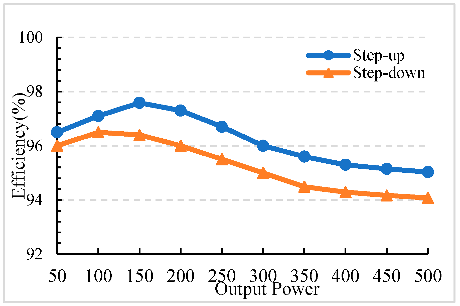
4. Experimental Results

The measured waveforms were used to verify the feasibility of the proposed topology. The key waveforms in the step-up and step-down modes were measured separately. Finally, the conversion efficiency of the proposed topology in the step-up and step-down modes were measured. Table 1 shows the electrical specifications and component parameters of the proposed topology, and a photograph of the proposed bidirectional isolated DC–DC converter is displayed in Figure 11.
Figure 12a–e shows the key waveforms measured in the step-up mode. Figure 12a displays the measured waveforms of the complementary signals vgs1 and vgs2,3 and the leakage inductance currents iLlk1 and iLlk2. Figure 12b depicts the measured waveforms of the voltage and current of the switches S1 and S2. These switches exhibited ZVS in the step-up mode, and their voltage stress was 100 V. Figure 12c illustrates the measured waveforms of the voltage and current of S3 and of the output voltage VH. The switch S3 exhibited ZVS in the step-up mode, and its voltage stress was 100 V. Figure 12d shows the measured waveforms of the voltage and current of S4 and S5. The voltage stress of these switches was 400 V. Figure 12e depicts the measured waveforms of the capacitors C1C4.
Figure 13a–e displays the key waveforms measured in the step-down mode. Figure 13a shows the measured waveforms of the complementary signals vgs1,5 and vgs2,3,4 and the leakage inductance currents iLlk1 and iLlk2. Figure 13b depicts the measured waveforms of the voltage and current of S1 and S2. The voltage stress of S1 and S2 was 100 V. Figure 13c displays the measured waveforms of the voltage and current of S3 and of the output voltage VH. The voltage stress of S3 was 100 V, and the output voltage of the converter was 48 V. Figure 13d shows the measured waveforms of the voltage and current of S4 and S5. These switches exhibited ZVS, and their voltage stress was 400 V. Figure 13e displays the measured waveforms of C1C4.
Figure 14 displays the conversion efficiency of the proposed converter in the step-up and step-down modes. The highest conversion efficiency in the step-up mode was 97.59% at 150 W, and the conversion efficiency at full load was 95.03%. The highest conversion efficiency in the step-down mode was 96.5% at 100 W, and the conversion efficiency at full load was 94.08%.
Table 2 presents a comparison between the proposed converter and those developed in [20,21,24,27,30]. In general, the proposed converter has fewer components, a higher efficiency, and a higher voltage gain than do the other converters, which indicates that the proposed converter can be widely used in numerous industries. Among the compared converters, the converter developed in [24] has the fewest components but has a low voltage gain and the lowest output power. Figure 15 and Figure 16 depict the voltage gain of the compared converters in the step-up and step-down modes, respectively. The converter developed in [27] has the highest voltage gain among all the compared converters but has a lower efficiency and a higher number of components than does the converter proposed in this paper. The converter in [30] has fewer switches but lower efficiency.
Figure 17 and Figure 18 depict the conversion efficiency of the compared converters in the step-up and step-down modes, respectively. The converter developed in [20] does not have a high conversion efficiency and has insufficient voltage gain. The converter developed in [21] has the highest output power but requires a highly complex control method. The converter developed in [24] has the highest efficiency but has a low output power and insufficient voltage gain. The converter developed in [27] has the highest voltage gain but has insufficient efficiency when the load level is less than half the full load and contains a high number of components. The converter in [30] has fewer components, but efficiency is lower. Finally, the converter proposed in this paper has a high conversion efficiency and voltage gain in the step-up and step-down modes.

5. Conclusions

In this paper, a novel high-efficiency bidirectional isolated DC–DC converter is proposed for an energy storage system. This converter only requires one complementary PWM signal to control the step-up and step-down modes. Partial switches are used in this converter to achieve ZVS, which can increase the converter efficiency. The feasibility of the proposed topology was examined through theoretical analysis, simulations, and experiments. In the experiments, the maximum efficiency of the proposed converter in the step-up and step-down modes was 97.59% and 96.5%, respectively.
In conclusion, the advantages of the proposed converter are as follows: (1) it has a simple circuit structure, (2) it only requires one complementary PWM signal to control the step-up and step-down modes, (3) it achieves a high voltage gain and high efficiency, (4) its input and output power supplies are separated through galvanic isolation, (5) the current of its low-voltage side is continuous in the CCM, and (6) ZVS is achieved using specific switches to reduce its switching loss.

Author Contributions

Conceptualization, Y.-E.W.; methodology, Y.-E.W. and K.-C.C.; formal analysis, Y.-E.W. and K.-C.C.; investigation, K.-C.C.; resources, Y.-E.W.; writing—original draft preparation, Y.-E.W. and K.-C.C.; writing—review and editing, Y.-E.W.; project administration, Y.-E.W.; funding acquisition, Y.-E.W. All authors have read and agreed to the published version of the manuscript.

Funding

This research received no external funding.

Institutional Review Board Statement

Not applicable.

Informed Consent Statement

Not applicable.

Data Availability Statement

All data utilized in this study are available online.

Conflicts of Interest

The authors declare no conflict of interest.

References

  1. Elavarasan, R.M.; Shafiullah, G.; Padmanaban, S.; Kumar, N.M.; Annam, A.; Vetrichelvan, A.M.; Mihet-Popa, L.; Holm-Nielsen, J.B. A Comprehensive Review on Renewable Energy Development, Challenges, and Policies of Leading Indian States with an International Perspective. IEEE Access 2020, 8, 74432–74457. [Google Scholar] [CrossRef]
  2. Jia, K.; Wang, C.; Bi, T.; Feng, T.; Zhu, R. Transient Current Correlation Based Protection for DC Distribution System. IEEE Trans. Ind. Electron. 2020, 67, 9927–9936. [Google Scholar] [CrossRef]
  3. Lucas, K.E.; Pagano, D.J.; Vaca-Benavides, D.A.; García-Arcos, R.; Rocha, E.M.; Medeiros, R.L.P.; Ríos, S.J. Robust Control of Interconnected Power Electronic Converters to Enhance Performance in DC Distribution Systems: A Case of Study. IEEE Trans. Power Electron. 2021, 36, 4851–4863. [Google Scholar] [CrossRef]
  4. Tesaki, K.; Hagiwara, M. Control and Experimental Verification of a Bidirectional Non-isolated DC–DC Converter Based on Switched-Capacitor Converters. IEEE Trans. Power Electron. 2021, 36, 6501–6512. [Google Scholar] [CrossRef]
  5. Mousavinezhad, S.; Sabahi, M. New Expandable Switched-Capacitor/Switched-Inductor High-Voltage Conversion Ratio Bidirectional DC–DC Converter. IEEE Trans. Power Electron. 2020, 35, 2480–2487. [Google Scholar]
  6. Sun, J.; Fong, Y.C.; Cheng, K.W.E. Current Source Mode Bidirectional DC/DC Converter with Multiple-Level Output Conversion Ratios Based on the Hybrid PWM Control of the Switched-Capacitor Structure. IEEE J. Emerg. Selected Topics Power Electron. 2022, 10, 604–616. [Google Scholar] [CrossRef]
  7. Wu, H.; Sun, K.; Chen, L.; Zhu, L.; Xing, Y. High Step-Up/Step-Down Soft-Switching Bidirectional DC–DC Converter with Coupled-Inductor and Voltage Matching Control for Energy Storage Systems. IEEE Trans. Ind. Electron. 2016, 63, 2892–2903. [Google Scholar] [CrossRef]
  8. Ardi, H.; Ajami, A.; Kardan, F.; Avilagh, S.N. Analysis and Implementation of a Non-isolated Bidirectional DC–DC Converter with High Voltage Gain. IEEE Trans. Ind. Electron. 2016, 63, 4878–4888. [Google Scholar] [CrossRef]
  9. Xiong, S.; Tan, S. Cascaded High-Voltage-Gain Bidirectional Switched-Capacitor DC–DC Converters for Distributed Energy Resources Applications. IEEE Trans. Power Electron. 2017, 32, 1220–1231. [Google Scholar] [CrossRef]
  10. Dung, N.A.; Chiu, H.-J.; Liu, Y.-C.; Huang, P.J. Analysis and Implementation of a High Voltage Gain 1 MHz Bidirectional DC–DC Converter. IEEE Trans. Ind. Electron. 2020, 67, 1415–1424. [Google Scholar] [CrossRef]
  11. Wai, R.; Liaw, J. High-Efficiency-Isolated Single-Input Multiple-Output Bidirectional Converter. IEEE Trans. Power Electron. 2015, 30, 4914–4930. [Google Scholar] [CrossRef]
  12. Mukhtar, N.M.; Lu, D.D. A Bidirectional Two-Switch Flyback Converter with Cross-Coupled LCD Snubbers for Minimizing Circulating Current. IEEE Trans. Ind. Electron. 2019, 66, 5948–5957. [Google Scholar] [CrossRef]
  13. Bai, C.; Han, B.; Kwon, B.; Kim, M. Highly Efficient Bidirectional Series-Resonant DC/DC Converter Over Wide Range of Battery Voltages. IEEE Trans. Power Electron. 2019, 35, 3636–3650. [Google Scholar] [CrossRef]
  14. Shi, H.; Sun, K.; Wu, H.; Li, Y. A Unified State-Space Modeling Method for a Phase-Shift Controlled Bidirectional Dual-Active Half-Bridge Converter. IEEE Trans. Power Electron. 2020, 35, 3254–3265. [Google Scholar] [CrossRef]
  15. Haneda, R.; Akagi, H. Design and Performance of the 850-V 100-kW 16-kHz Bidirectional Isolated DC–DC Converter Using SiC-MOSFET/SBD H-Bridge Modules. IEEE Trans. Power Electron. 2020, 35, 10013–10025. [Google Scholar] [CrossRef]
  16. Waffler, S.; Kolar, J.W. A Novel Low-Loss Modulation Strategy for High-Power Bidirectional Buck + Boost Converters. IEEE Trans. Power Electron. 2009, 24, 1589–1599. [Google Scholar] [CrossRef]
  17. Jia, L.; Sun, X.; Zheng, Z.; Ma, X.; Dai, L. Multimode Smooth Switching Strategy for Eliminating the Operational Dead Zone in Noninverting Buck–Boost Converter. IEEE Trans. Power Electron. 2020, 35, 3106–3113. [Google Scholar] [CrossRef]
  18. Lee, H.-S.; Yun, J.-J. High-Efficiency Bidirectional Buck–Boost Converter for Photovoltaic and Energy Storage Systems in a Smart Grid. IEEE Trans. Power Electron. 2019, 34, 4316–4328. [Google Scholar] [CrossRef]
  19. Méndez-Díaz, F.; Pico, B.; Vidal-Idiarte, E.; Calvente, J.; Giral, R. HM/PWM Seamless Control of a Bidirectional Buck–Boost Converter for a Photovoltaic Application. IEEE Trans. Power Electron. 2019, 34, 2887–2899. [Google Scholar] [CrossRef]
  20. Zhang, Y.; Liu, Q.; Gao, Y.; Li, J.; Sumner, M. Hybrid Switched-Capacitor/Switched-Quasi-Z-Source Bidirectional DC–DC Converter with a Wide Voltage Gain Range for Hybrid Energy Sources EVs. IEEE Trans. Ind. Electron. 2019, 66, 2680–2690. [Google Scholar] [CrossRef]
  21. Zhang, Y.; Zhang, W.; Gao, F.; Gao, S.; Rogers, D.J. A Switched-Capacitor Interleaved Bidirectional Converter with Wide Voltage-Gain Range for Super Capacitors in EVs. IEEE Trans. Power Electron. 2020, 35, 1536–1547. [Google Scholar] [CrossRef]
  22. Santra, S.B.; Chatterjee, D.; Liang, T.-J. High Gain and High-Efficiency Bidirectional DC–DC Converter with Current Sharing Characteristics Using Coupled Inductor. IEEE Trans. Power Electron. 2021, 36, 12819–12833. [Google Scholar] [CrossRef]
  23. Akhormeh, A.R.N.; Abbaszadeh, K.; Moradzadeh, M.; Shahirinia, A. High-Gain Bidirectional Quadratic DC–DC Converter Based on Coupled Inductor with Current Ripple Reduction Capability. IEEE Trans. Ind. Electron. 2021, 68, 7826–7837. [Google Scholar] [CrossRef]
  24. Rezvanyvardom, M.; Mirzaei, A. Zero-Voltage Transition Non-isolated Bidirectional Buck–Boost DC–DC Converter with Coupled Inductors. IEEE J. Emerg. Sel. Topics Power Electron. 2021, 9, 3266–3275. [Google Scholar] [CrossRef]
  25. Zhang, F.; Yan, Y. Novel Forward–Flyback Hybrid Bidirectional DC–DC Converter. IEEE Trans. Ind. Electron. 2009, 56, 1578–1584. [Google Scholar] [CrossRef]
  26. Zeng, J.; Yan, Z.; Liu, J.; Huang, Z. A High Voltage-Gain Bidirectional DC–DC Converter with Full-Range ZVS Using Decoupling Control Strategy. IEEE J. Emerg. Sel. Topics Power Electron. 2020, 8, 2775–2784. [Google Scholar] [CrossRef]
  27. Wu, Y.-E.; Ke, Y.-T. A Novel Bidirectional Isolated DC-DC Converter with High Voltage Gain and Wide Input Voltage. IEEE Trans. Power Electron. 2021, 36, 7973–7985. [Google Scholar] [CrossRef]
  28. PTomar, S.; Srivastava, M.; Verma, A.K. An Improved Current-Fed Bidirectional DC–DC Converter for Reconfigurable Split Battery in EVs. IEEE Trans. Appli. Electron. 2020, 56, 6957–6967. [Google Scholar]
  29. Lu, Y.; Wu, Q.; Wang, Q.; Liu, D.; Xiao, L. Analysis of a Novel Zero-Voltage-Switching Bidirectional DC/DC Converter for Energy Storage System. IEEE Trans. Power Electron. 2018, 33, 3169–3179. [Google Scholar] [CrossRef]
  30. Wu, Y.E.; Pan, B.H. High Efficiency and Voltage Conversion Ratio Bidirectional Isolated DC-DC Converter for Energy Storage System. IEEE Access 2022, 10, 55187–55199. [Google Scholar] [CrossRef]
Figure 1. Configuration of a distributed generation system with an energy storage system.
Processes 10 02711 g001
Figure 2. Voltage polarity and current direction of the components of the proposed topology.
Processes 10 02711 g002
Figure 3. Key waveforms of the proposed topology in the step-up mode.
Processes 10 02711 g003
Figure 4. Equivalent circuits in the step-up mode: (a) Mode 1, (b) Mode 2, (c) Mode 3, (d) Mode 4, and (e) Mode 5.
Processes 10 02711 g004
Figure 5. Key waveforms of the proposed topology in the step-down mode.
Processes 10 02711 g005
Figure 6. Equivalent circuits in the step-down mode: (a) Mode 1, (b) Mode 2, (c) Mode 3, (d) Mode 4, (e) Mode 5, (f) Mode 6, and (g) Mode 7.
Processes 10 02711 g006
Figure 7. Relationship between the voltage gain and the duty cycle in the step-up mode.
Processes 10 02711 g007
Figure 8. Plot of the voltage gain versus the duty cycle in the step-down mode.
Processes 10 02711 g008
Figure 9. Lm1, BCM in the step-up mode.
Processes 10 02711 g009
Figure 10. Lm1, BCM in step-down mode.
Processes 10 02711 g010
Figure 11. Photograph of the proposed converter.
Processes 10 02711 g011
Figure 12. Experimental results obtained when operating the proposed converter at full load and a VL value of 48 V in the step-up mode: (a) waveforms of vgs1, vgs2,3, iLlk1, and iLlk2; (b) waveforms of the vds and is values of S1 and S2; (c) waveforms of the vds and is values of S3 and of the output voltage; (d) waveforms of the vds and is values of S4 and S5; and (e) waveforms of the voltages of C1, C2, C3, and C4.
Processes 10 02711 g012
Figure 13. Experimental results obtained when operating the proposed converter at full load and a VH value of 400 V in the step-down mode: (a) waveforms of vgs1,5, vgs2,3,4, iLlk1, and iLlk2; (b) waveforms of the vds and is values of S1 and S2; (c) waveforms of the vds and is values of S3 and of the output voltage; (d) waveforms of the vds and is values of S4 and S5; and (e) waveforms of the voltages of C1, C2, C3, and C4.
Processes 10 02711 g013
Figure 14. Efficiency of the proposed converter.
Processes 10 02711 g014
Figure 15. Voltage gain of the compared converters in the step-up mode.
Processes 10 02711 g015
Figure 16. Voltage gain of the compared converters in the step-down mode.
Processes 10 02711 g016
Figure 17. Efficiency of the compared converters in the step-up mode.
Processes 10 02711 g017
Figure 18. Efficiency of the compared converters in the step-down mode.
Processes 10 02711 g018
Table 1. Electrical Specifications of the Proposed Topology.
ParameterSpecification
High-side power PH500 W
Low-side power PL500 W
High-side voltage VH400 V
High-side current IH1.25 A
Low-side voltage VL48 V
Low-side current IL10.416 A
Switching frequency fs40 kHz
Power switches S1, S2 and S3IRFP4568
Power switches S4 and S5IXFH60N50P3
Magnetizing inductance Lm1200 µH
Leakage inductance Llk1 and Llk22 µH
Capacitor C1, C2, C3 and C450 µF
Turns ratio n4
Table 2. Comparison between the proposed converter and related bidirectional converters.
Converter in [20]Converter in [21]Converter in [24]Converter in [27]Converter in [30]Proposed
Converter
G s t e p u p ( V H V L ) 2 + D ( 1 D ) 3 ( 1 D ) 3 D + n n ( 1 D ) n ( 1 D ) 2 n ( 1 D ) n ( 1 D )
G s t e p d o w n ( V L V H ) D ( 3 D ) D 3 n D n + 3 ( 1 D ) ( 1 D ) 2 n 1 D n 1 D n
VL40–120 V30–100 V48 V24–48 V48 V48 V
VH400 V400 V120 V400 V400 V400 V
Switches584645
Magnetic Components232211
Capacitors660344
Diodes001000
Efficiency of step-up mode94.09%95.8%98%95.6%96.8%97.59%
Efficiency of step-down mode94.41%95.9%97%94.2%95.2%96.5%
IsolatedNoNoNoYesYesYes
Publisher’s Note: MDPI stays neutral with regard to jurisdictional claims in published maps and institutional affiliations.

