Review

From 1D to 2D to 3D: Electrospun Microstructures towards Wearable Sensing

1
Collaborative Innovation Center of Advanced Microstructures, School of Electronic Science and Engineering, Nanjing University, Nanjing 210093, China
2
Department of Materials Process Engineering, Graduate School of Engineering, Nagoya University, Nagoya 464-8603, Japan
3
School of Microelectronics and Control Engineering, Changzhou University, Changzhou 213164, China
*
Authors to whom correspondence should be addressed.
Chemosensors 2023, 11(5), 295; https://doi.org/10.3390/chemosensors11050295
Submission received: 13 March 2023 / Revised: 9 May 2023 / Accepted: 12 May 2023 / Published: 16 May 2023
(This article belongs to the Section Materials for Chemical Sensing)

Abstract

:
Wearable sensors open unprecedented opportunities for long-term health monitoring and human–machine interaction. Electrospinning is considered to be an ideal technology to produce functional structures for wearable sensors because of its unique merits to endow devices with highly designable functional microstructures, outstanding breathability, biocompatibility, and comfort, as well as its low cost, simple process flow, and high productivity. Recent advances in wearable sensors with one-, two-, or three-dimensional (1D, 2D, or 3D) electrospun microstructures have promoted various applications in healthcare, action monitoring, and physiological information recognition. Particularly, the development of various novel electrospun microstructures different from conventional micro/nanofibrous structures further enhances the electrical, mechanical, thermal, and optical performances of wearable sensors and provides them with multiple detection functions and superior practicality. In this review, we discuss (i) the principle and typical apparatus of electrospinning, (ii) 1D, 2D, and 3D electrospun microstructures for wearable sensing and their construction strategies and physical properties, (iii) applications of microstructured electrospun wearable devices in sensing pressure, temperature, humidity, gas, biochemical molecules, and light, and (iv) challenges of future electrospun wearable sensors for physiological signal recognition, behavior monitoring, personal protection, and health diagnosis.

1. Introduction

Wearable sensors are technological devices that can be worn on the body to collect and monitor data about an individual’s physiological, behavioral, and environmental characteristics [1,2,3,4,5,6,7,8,9,10,11]. These sensors have the potential to significantly impact human life in health monitoring, fitness tracking, security, and human–machine interaction [12,13,14,15]. These sensors have become increasingly popular in recent years, with many commercial products now available on the market [16,17]. Present-day commercially available wearables are capable of continuously monitoring an individual’s physiological signals under typical daily conditions [7]. The captured biological signals are vital for assessing the health of wearers, particularly for older adults and individuals with chronic illnesses, and athletes’ performance analysis [18,19]. One drawback of wearable sensors, including smartwatches, bands, and apparel-based gadgets, is that they are hard, heavy, and performantly inferior, resulting in poor wearing comfort and weak signals [20,21]. This limitation can be solved by current flexible electronic devices, which can create conformable contact with the human skin, improving the sensing performances, practicality, and comfort [22,23]. However, common flexible electronic sensors in the form of dense films and patches are airtight, which may pose a risk of inflammation and discomfort during long-term use [24]. Meanwhile, to realize fast sensitive response, complex processes and expensive manufacturing equipment are required to create functional interfaces with large specific surface areas and special microstructures, limiting their development and industrialization [25,26].
The emergence of electrospun wearable sensors can conquer these problems due to their outstanding breathability, biocompatibility, flexibility, comfort, high specific surface area, low cost, and ease of large-scale fabrication [27,28]. It has been demonstrated that the robust, dynamic electrospun wearable sensor makes bioelectronics capable of monitoring real-time, continuous physiological, bioelectrical, and biochemical signals in an imperceptible way [29]. The electrospun wearable sensor allows for continuous and long-term health monitoring by collecting high-quality, real-time data on vital bio-signals [30]. This includes human activity, body temperature, cardiac mapping, electrophysiological signals, and molecular analysis of body fluids and exhaled breath, as well as external environmental conditions, such as humidity and ultraviolet (UV) intensity. The gathered biometric data enable comprehensive health status analysis, offering a valuable tool for predicting and preventing diseases, conducting screenings and diagnoses, and providing treatment in a convenient and non-intrusive manner [31]. Furthermore, it is easy to adjust the size of electrospun microstructures and construct various electrospun microstructures with rich geometric configurations to regulate and optimize the performances of corresponding wearable devices in sensing pressure, temperature, humidity, gas, biochemical molecules, and light [32,33,34]. Therefore, it is necessary to provide a bird’s eye-view of electrospun wearable sensors with a focus on their production strategies and comprehensive applications. The knowledge and insights rendered in this review will arouse interest within the scientific community in two aspects: (i) promote the development of electrospun microstructures for high-performance, comfortable, stable, advanced wearable sensing textiles; and (ii) track the progress of all types of wearable sensors towards physiological signal recognition, behavior monitoring, personal protection, and health diagnosis. Additionally, this review will attract remarkable attention from researchers in the fields of flexible electronics and biomedicine, as well as users, healthcare funders, sensing-tech giants, and wearable device providers.
This review begins with a description of electrospinning principles and representative apparatuses for producing wearable electrospun sensors and then elaborates construction strategies and physical properties of 1D, 2D, and 3D electrospun microstructures for wearable sensing towards behavior monitoring, healthcare, and disease diagnosis. The review will also highlight promising real-life applications of microstructured electrospun devices in sensing pressure, temperature, gas, humidity, biochemical molecules, and light. We then conclude with a summary of the challenges, opportunities, and future directions in the field of constructing electrospun microstructures for advanced wearable sensors.

2. Electrospinning Principles and Typical Apparatuses

2.1. Principle and Process

Electrospinning is a flexible technique to produce efficiently various polymer-containing fibers with diameters ranging from nanometers to micrometers [35,36,37,38]. Its principle is based on the interaction between electrostatic field force and surface tension [2,5,39]. When a high voltage is applied to the electrospinning liquid precursor, the electrostatic repulsion among the surface charges with the same sign distorts the liquid into the conical shape, known as the “Taylor cone” [40,41]. Subsequently, once the electrostatic repulsion overcomes the surface tension of the electrified liquid precursor, the liquid precursor is ejected in the form of the jet [3,4,6]. Initially, the jet moves in a straight line along the direction of the electric field, but it subsequently experiences vigorous whipping motions due to bending instabilities [36,42,43,44]. The linear motion distance of the jet, in general, is within 1 cm (Figure 1a). At the same time, the jet gradually solidifies as it is stretched into a smaller diameter [1]. Finally, the jet or the solidified fiber crashes against the collector [45,46].

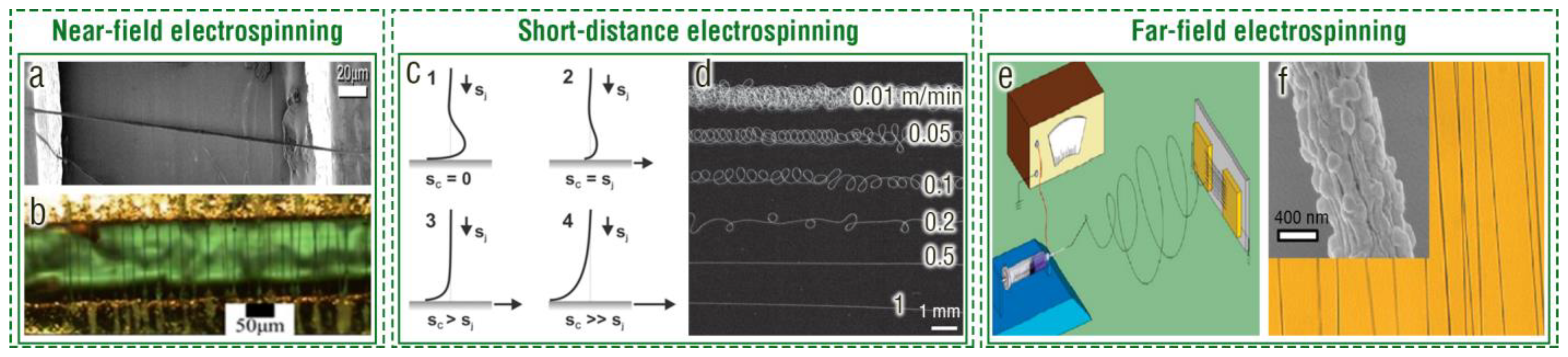
2.2. Typical Apparatuses

To produce various ultrathin fibers, the most basic apparatus of electrospinning typically includes a high-voltage power supply, a syringe pump, a spinneret (usually, a metal needle), and a collector (Figure 1a) [15,50,51]. The high-voltage power supply connected to the needle creates an electric field between the needle and the collector to accelerate the jet [52]. The syringe pump controls the flow rate of the electrospinning liquid precursor from the needle [36]. The spinneret is the source of the electrospinning liquid precursor and dispenses the liquid precursor [53]. The collector is used to attract the electrified electrospun fiber [54]. The collector is usually grounded or connected to a high voltage source with the opposite charge sign of the spinneret. Since the instability of the jet is gradually aggravated with the increase in the distance the jet is moving, significant differences in the morphology and physical properties of the collected electrospun textile appear with the change in the distance between the spinneret and the collector [55]. The electrospinning apparatuses first can be categorized as near-field electrospinning (NFES), short-distance electrospinning (SDES, also known as medium-field electrospinning) [56], or far-field electrospinning (FFES) according to the difference of the collecting distance [57]. NFES has a very short distance between the spinneret and the collector, typically less than 1 cm (Figure 1b) [57]. Within such a short distance, the jet can maintain a linear motion [58]. Therefore, NFES allows for more precise control over the jet, resulting in a higher resolution and more uniform fibers [59]. In addition to preparing highly desirable 1D ultrathin fibers, NFES is even used for fabricating some 3D structures due to its high precision and accuracy [60]. Moreover, the ultrahigh electric field of NFES can strongly align the dipoles of polar materials, effectively triggering piezoelectric effect for ferroelectrics [28]. The distance between the spinneret and the collector for SDES is typically between 1 cm and 8 cm (Figure 1c). The shorter distance between the spinneret and the collector allows for a denser fiber deposition and enables the production of thicker fibers compared with far-field electrospinning. In addition, assembled with a high-speed drum collector, SDES is capable of producing well-aligned fiber bundles [61]. FFES is a technique where the distance between the spinneret and the collector, in general, is not less than 8 cm (Figure 1d) [1]. This distance allows for more controlled and stable jet formation, which results in a more efficient and productive process [62,63]. The following subsections provide a brief account of the important components typically applied in NFES, SDES, and FFES for electrospun microstructure constructures.

2.2.1. High-Voltage Power Supply

There are two types of high-voltage power supplies commonly used in electrospinning: (i) direct current (DC) power supply and (ii) alternating current (AC) power supply [64,65]. The DC power supply is the most basic type of high-voltage power supply used in electrospinning. It typically provides a voltage output ranging from a few hundred volts to several kilovolts [66]. This type of power supply is the most common and widely used device because it is relatively inexpensive and easy to operate [67]. Unlike DC power supplies, AC power supplies provide a time-varying voltage output that can help produce more uniform fibers. This is mainly because the AC power supply induce the charges to be transferred back and forth along the jet, which weakens the Coulomb repulsive force acting on the following jet and, therefore, the whipping instability [68].

2.2.2. Spinneret

The spinneret is a critical component of electrospinning, as it determines the resulting microarchitectures of the prepared materials to a large extent. Various spinnerets possess their own characteristics for electrospinning. Five types of common spinnerets, including (i) single-needle spinneret, (ii) multi-jet spinneret with various mechanical and array structures, (iii) coaxial spinneret, (iv) triaxial spinneret, and (v) multi-channel spinneret, are systematically described. The single-needle spinneret usually has a blunt tip (Figure 2a) which is used typically to produce randomly oriented fibers [62], aligned fibers [69], and various self-assembled electrospun microstructures [1,2,3,4,5,6,37]. The alignment and diameter of the prepared fibers can be well controlled by adjusting the electrospinning parameters, such as the electrostatic field strength and solution flow rate [70]. In contrast to the single-needle spinneret that commonly emits a single jet from the Taylor cone, the multi-jet spinneret is used to emit multiple jets, leading to a more uniform distribution of electrospun fibers and higher production rates. Multi-jet spinnerets include needleless spinnerets and multiple-needle spinnerets. Needleless spinnerets have all types of sharps, for example pyramid- (Figure 2b) [71], disk- (Figure 2c) [50], cylinder- (Figure 2d) [72], tube- (Figure 2e) [73], spiral- (Figure 2f) [74], ball- (Figure 2g) [75], and wire-shaped [76](Figure 2h) spinnerets. The multiple-needle spinneret consists of two or more needles arranged in various ways (Figure 2i) [77,78]. Due to the complex structure of spinnerets and mutual interference of multiple jets, the diameter and alignment of the fibers prepared by means of multi-jet spinnerets may not be as controllable as with a single-needle spinneret [79]. The coaxial spinneret can produce core–shell [80], hollow [81], and porous [82] fibers with controlled diameters and shell thicknesses. In this type of spinneret, the polymer solution or oil is dispensed through an inner needle, while a sheath fluid is dispensed through an outer needle (Figure 2j) [80,81,82]. Similarly, the triaxial spinneret with three concentrically arranged spinnerets can produce fibers with core–shell–shell [83] and wire-in-tube [84] structures. The innermost spinneret is used to dispense a core solution, which is surrounded by a middle spinneret that dispenses a shell solution or oil and then a third outermost spinneret that dispenses (another) shell solution (Figure 2k) [83,84]. Moreover, the multi-channel spinneret is capable of fabricating fibers with multi-channel microtube and multicomponent microcapsule structures (Figure 2l) [85].

2.2.3. Collector

A wide variety of collectors can be chosen to fabricate desired electrospun microstructures. The conducting plate or mesh collector (Figure 3a) is the most common type of collector used in electrospinning due to its simplicity. Additionally, many other more complex collectors have been developed. High-speed rotator collectors, such as rotating drums [37] (Figure 3b), rotating wire drums [86] (Figure 3c), and rotating disks [87] (Figure 3d), are usually utilized to produce aligned fibers by applying mechanical force during the collecting process. The roll-to-roll collector involves a continuous collection of electrospun fibers onto a rotating cylinder or drum (Figure 3e), which allows for high throughput production and can easily be scaled up for industrial use [15]. Parallel electrode collectors, such as horizontal substrates [42,88] (Figure 3f) and dual rings [89] (Figure 3g), can also help create aligned fibers. Some 3D-architectured collectors, such as columnar- [41] (Figure 3h) and spring-shaped (Figure 3i) collectors as templates, are used to make corresponding 3D fibrous constructs, for example, nanofibrous tubes.
Assembling special devices to and near the collector is also an effective approach to obtain desired micro/nanoarchitectured electrospun textiles. For instance, adding a pair of thin polyimide films positioned a few millimeters away from a rotating cylindrical collector can redirect the airflow generated by the collector’s rotation and concentrate the electric field onto the gap between them, resulting in precise control over the alignment of the fiber bundles (Figure 3j) [61]. Assembling electrodes connected to a signal generator near the collector can deflect a polymer jet onto a substrate in a controlled pattern by stacking nanofibers on top of each other, which is used to print complex submicron-featured 3D objects with high precision and accuracy (Figure 3k) [59]. When a rotating and charged mandrel is placed asymmetrically between two charged plates, electrospun fibers with larger diameters can be oriented circumferentially to the longitudinal axis of a tubular structure, while small-diameter fibers are randomly oriented (Figure 3l). Moreover, an auxiliary electrical field can be employed when a charged auxiliary electrode made of a plurality of connected aluminum foil strips is placed several centimeters away from the drum collector. This auxiliary electrical field can be used to achieve substantial circumferential orientation of deposited fibers (Figure 3m) [90]. In addition, adding an electrostatic lens consisting of a series of charged rings to the traditional electrospinning apparatus can exert multiple field effect to the moving jet and, therefore, reduce its whipping instability. The jet can be straightened, to some extent, in this process, and nicely aligned fiber yarns even can be collected (Figure 3n) [91]. In addition to being placed in air, the collector can be placed in liquid to prepare porous electrospun fibers (Figure 3o) [92]. Electrospun fibers can deposit not only on specific collectors but also on almost all solid surfaces. Even the skin can serve as a collector (Figure 3p) [93].
Figure 3. Various collectors for producing different electrospun microstructures. (a) Schematic diagram of the conducting plate collector. (Reprinted with permission from Ref. [37]. Copyright 2020, IOP Publishing Ltd.) (b) Schematic diagram of the rotating drum collector. (Reprinted with permission from Ref. [3]. Copyright 2020, Elsevier.) (c) Schematic diagram of the rotating wire drum collector. (Reprinted with permission from Ref. [86]. Copyright 2004, American Chemical Society.) (d) Schematic diagram of the rotating disk collector. (Reprinted with permission from Ref. [87]. Copyright 2003, AIP Publishing LLC.) (e) Schematic of the roll-to-roll collector. (Reprinted with permission from Ref. [15]. Copyright 2021, Springer Nature.) (f) Schematic of the horizontal parallel electrode collector. (Reprinted with permission from Ref. [88]. Copyright 2004, Wiley-VCH.) (g) Schematic of the dual ring parallel electrode collector. (Reprinted with permission from Ref. [89]. Copyright 2005, Elsevier.) (h) Schematic of the dual ring parallel electrode collector. (Reprinted with permission from Ref. [41]. Copyright 2008, American Chemical Society.) (i) Schematic of the columnar-shaped collector. (Reprinted with permission from Ref. [41]. Copyright 2008, American Chemical Society.) (h) Schematic of the spring-shaped collector. (Reprinted with permission from Ref. [94]. Copyright 2017, Wiley-VCH.) (j) Schematic showing a drum collector assembled with a pair of thin polyimide films (Reprinted with permission from Ref. [61]. Copyright © 2017 Wiley-VCH.) (k) Schematic showing jet-deflecting electrodes assembled near the plate collector. (Reprinted with permission from Ref. [59]. Open access Creative Common CC licensed 4.0, Springer Nature.) (l) Schematic showing two charged plates assembled near the charged mandrel collector. (m) Schematic showing a charged auxiliary electrode assembled near the charged drum collector. (n) Schematic showing three charged rings assembled near the charged plate collector. (Reprinted with permission from Ref. [91]. Copyright 2001, Elsevier.) (o) Schematic showing a plate collector placed in liquid. (Reprinted with permission from Ref. [92]. Copyright © 2006 American Chemical Society.) (p) Schematic diagram showing skin serving as a collector. (Reprinted with permission from Ref. [93]. Copyright © 2016 Royal Society of Chemistry).
Chemosensors 11 00295 g003

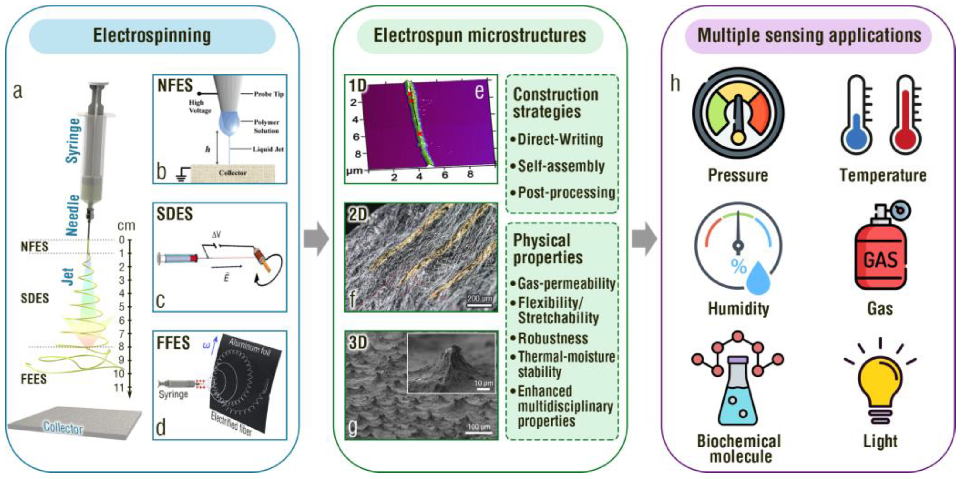
3. Construction Strategies and Physical Properties of Electrospun Textiles

Microstructures, to a large extent, determine the performances of sensors in detecting pressure, temperature, humidity, gas, biochemical molecules, and light [63,95,96,97,98,99,100,101,102,103]. Electrospun textiles with inherent biocompatibility, breathability, waterproofness, mechanical durability, and thermal–moisture stability are ideal materials to meet the increasingly urgent demands in wearable functional devices [24,29,30,38,54]. Therefore, it is highly desired to develop electrospun textiles with special microstructures to achieve high-performance wearable sensors [104]. In this section, we will discuss the construction strategies of 1D, 2D, and 3D electrospun microstructures and the unique advantages of microstructured electrospun textiles in breathability, flexibility, stretchability, robustness, thermal–moisture stability, imperceptibility, and transparency. Representative examples are exhibited, with a focus on discussion and comparison of the merits of various construction strategies and designs.

3.1. Construction Strategies

In the following subsections, we discuss the construction strategies of 1D electrospun fibers, 2D electrospun textiles, and 3D electrospun microstructures, respectively. Some typical strategies for constructing 3D electrospun microstructures are extensively discussed owing to their specificity of morphology and difficulty of preparation. Notably, the division of electrospinning material dimensions often causes confusion because there is no uniform standard. In this review, we defined 1D, 2D, and 3D electrospun materials, relying mainly on the standard which dominates the particular functions of each of the 1D, 2D, or 3D structural properties.

3.1.1. One-Dimensional Electrospun Fibers

One-dimensional electrospun fibers refer to a single fiber (Figure 4a) or several fibers (Figure 4b) that cannot compose a film. Since the moving speed of the jet in electrospinning usually is ultrafast (from several tens to several hundreds of meters per second) and a large number of electrospun fibers can be collected in a very short time [28], 1D electrospun fibers, in general, are fabricated by NFES rather than SDES or FFES. Chang et al. used near-field electrospinning to direct-write poly(vinylidene fluoride) (PVDF) fibers with in situ mechanical stretch and electrical poling characteristics. The prepared single electrospun fiber with a diameter ranging from 500 nm to 6.5 µm was rendered with excellent piezoelectricity due to the in situ stretch and poling process [105]. Fuh et al. fabricated approximately 500 parallel electrospun PVDF fibers with an average diameter of 2.5 μm onto metallic electrodes for preparing a piezoelectric nanogenerator (PENG) [106]. It is noted that NFES is an ideal approach to direct-write highly designable electrospun fibers with relatively large fiber diameters, typically to the micron level.
Although there exist some difficulties in preparing 1D electrospun fibers by SDES and FFES due to a large spinneret–collector distance, this difficulty can be conquered by retrofitting traditional SDES and FFES apparatuses. Brown et al. found that the relationship between jet speed and collector speed influenced the alignment of collected fibers [106]. When the collector was not moving, the jet deposition location diverged away from the point directly below the spinneret due to coiling caused by compressive forces along the jet once the jet crashed against the collector [2]. A 2D fibrous network was obtained in this case. With the increase of the collector moving speed, the net effect of the compressive force became weaker owing to an axial tensile force acting on the jet, which stemmed from the drag between the jet and the collector. Once the collector moving speed was equal to the jet speed, a balance between the compressive force and the tensile force was realized, and, therefore, the deposition point was directly below the spinneret (Figure 4c). A straight 1D electrospun fiber of micron-level diameter was successfully fabricated (Figure 4d). When the speed of the collector exceeded that of the jet, the jet was stretched because the drag surpassed the compressive stresses. The average diameter of the obtained fiber was reduced. This condition was intensified with a further increase in the collector speed. To fabricate 1D electrospun fibers with nanoscale diameters, modified FFES was used. Hansen et al. reported that when two grounded copper pieces with a 2 cm gap was used as the collector and the spinneret–collector distance was 15 cm, the nanofibers were aligned across the gap of these two copper pieces (Figure 4e,f) [107]. The reason was that an insulating gap between the electrode collector changed both the electrostatic field structure and the electrostatic force direction acting on the jets [88]. Meanwhile, induced charges on the electrodes further attracted the fiber to locate across the insulating gap [1].
Figure 4. One-dimensional electrospun fibers constructed by NFES, SDES, and FFES. (a) SEM image of a single nanofiber fabricated by NFES. (Reprinted with permission from Ref. [105]. Copyright 2011, American Chemical Society.) (b) SEM image of dozens of fibers independent of each other, which are fabricated by NFES. (Reprinted with permission from Ref. [106]. Copyright 2015, American Chemical Society.) (c) Schematic showing that the shape of the melt electrospinning jet profile is dependent on the speed of the collector (SC) relative to the jet speed (SJ). (d) Photograph showing the 1D fibers fabricated by SDES with different moving speeds of the collector. (Reprinted with permission from Ref. [108]. Copyright 2011, Wiley-VCH.) (e) Schematic diagram of a FFES apparatus to fabricate 1D fibers. (f) Photograph and SEM image of the 1D fibers fabricated by FFES. (Reprinted with permission from Ref. [107]. Copyright 2010, American Chemical Society).
Chemosensors 11 00295 g004

3.1.2. Two-Dimensional Electrospun Textiles

In general, for ease of description, the 2D electrospun textile is roughly defined as an ultrathin network (Figure 5a) and a relatively thick mat with relatively flat surfaces (Figure 5b) [1,3]. The 2D non-woven textile is the most common electrospun structure, which can be divided into two types: the film composed of (i) randomly oriented and (ii) regularly aligned electrospun fibers. FFES and SDES are usually used to fabricate randomly oriented electrospun fiber textiles with different thicknesses. Choosing appropriate electrospinning time is the most effective and simplest approach to produce 2D electrospun textiles with desired thicknesses ranging from tens of nanometers to a few millimeters [4]. Wu et al. utilized FFES with a copper ring as the collector to prepare ultrathin 2D electrospun textiles consisting of randomly oriented water-soluble polymer nanofibers [109]. After metal is deposited on this 2D electrospun network and the polymer template is dissolved, a metal network with nanotroughs interconnected at their junctions is prepared (Figure 5c,d). Wang et al. also constructed ultrathin 2D electrospun polyurethane (PU) networks based on randomly oriented nanofibers by FFES with a silicone-coated paper attached to the grounded collector for easy delamination [104]. The as-prepared 2D electrospun networks were immersed in polydimethylsiloxane (PDMS) solution to connect junctions of electrospun PU nanofibers, producing interconnected nanofiber meshes (Figure 5e). Ni et al. used a systematic method involving the sequential processes of FFES, welding, and dry-annealing to produce interconnected nanofiber-based electrospun PVA mats (Figure 5f,g) [110]. The interfaces between nanofibers were welded by a post-treatment of water vapor exposure. Since connecting the junctions of electrospun nanofibers can significantly improve both mechanical and electrical properties of 2D electrospun textiles but requires tedious steps [104,109,110], there is a necessity to develop one-step self-assembled interconnected nanofiber-based textiles for simplification of the fabrication process. Zhang et al. developed a direct electronetting technology to self-assemble interconnected nanofiber-based networks from various materials [43]. An FFES apparatus included a dielectric electrospun mesh as the collector and the very dilute polymer solution as liquid precursor [111]. This set-up tailors the precursor solution and microelectric field, enabling charged droplets to levitate, deform, and phase-separate to form the resulting interconnected fibrous 2D structure (Figure 5h,i) [112].
Compared with the textile composed of randomly oriented fibers, the well-aligned fiber-based electrospun textile, in general, possesses special effects and higher performances in sensing [28]. NFES, SDES, and FFES can all be used to prepare regularly aligned fiber-based 2D electrospun textiles [51,69]. Direct-writing electrospinning techniques that are based on NFES and SDES are the most precise but most inefficient approach to produce this type of electrospun textile [113]. Huang et al. reported that NFES can be used directly to direct-write various patterned 2D textiles (Figure 5j,k) [56]. Moreover, with optimal control so that the collector moves at speeds matching the jet speed, SDES can also be used to regularly direct-write melt fiber to form patterned 2D electrospun mats (Figure 5l) [108]. To significantly improve production efficiency, assembled with a cylindrical collector rotating at high speed (usually reaching up to thousands of rpm), both SDES and FFES can be used to yield roughly uniaxially aligned fiber-based 2D electrospun films [114]. This is because the high-speed collector applies a mechanical force to straighten the crimped fibers. Assembling patterned electrodes onto the high-speed cylindrical collector can further improve the orientation of uniaxially aligned fibers due to the optimized electrostatic field distribution (Figure 5m,n) [69]. There are still other collectors and designs to produce well-aligned fiber-based 2D electrospun films by SDES and FEES, which have been described in Section 2.2.3. Notably, stacking two layers of uniaxially aligned nanofibers with a certain rotation angle can produce a mesh comprising biaxially aligned nanofibers (Figure 5o) [42].
Figure 5. Two-dimensional electrospun textiles constructed by NFES, SDES, and FFES. (a) SEM image of a typical ultrathin electrospun network with relatively flat surface. (Reprinted with permission from Ref. [115]. Copyright 2010, American Chemical Society.) (b) SEM image of a typical relatively thick mat with relatively flat surface. (Reprinted with permission from Ref. [2]. Copyright 2011, American Chemical Society.) (c) Schematic of the preparation process of the 2D metal nanotrough network by means of FFES. (d) Photograph showing ultrathin 2D electrospun textile consisting of randomly oriented fibers prepared by FFES. (Reprinted with permission from Ref. [109]. Copyright 2013, Springer Nature.) (e) Schematic diagrams, photographs, and SEM images of the ultrathin 2D electrospun PU network based on randomly oriented nanofibers and the PU-PDMS core–sheath nanomesh. (Reprinted with permission from Ref. [104]. Open access Creative Common CC licensed 4.0, American Association for the Advancement of Science.) (f) Schematic diagram of the preparation process of interconnected nanofiber-based electrospun PVA mats. (g) SEM image of an interconnected nanofiber-based electrospun PVA mat. (Reprinted with permission from Ref. [110]. Copyright 2021, Elsevier.) (h) Schematic diagram of the apparatus and mechanism to produce an interconnected fibrous 2D net. (Reprinted with permission from Ref. [112]. Open access Creative Common CC licensed 4.0, Springer Nature.) (i) SEM image of the interconnected fibrous 2D net fabricated by the self-assembly electronetting technology. (Reprinted with permission from Ref. [43]. Open access Creative Common CC licensed 4.0, Springer Nature.) (j) Schematic diagram of an NFES apparatus that is direct-writing a pattern-controlled 2D textile. (Reprinted with permission from Ref. [113]. Copyright 2022 American Chemical Society.) (k) SEM image of a 2D electrospun textile composed of regularly aligned fibers. (Reprinted with permission from Ref. [56]. Copyright 2013, Royal Society of Chemistry.) (l) SEM image of a patterned 2D electrospun mat consisting of well-aligned fibers. (Reprinted with permission from Ref. [108]. Copyright 2011, Wiley-VCH.) (m) Schematic diagram of the FFES apparatus for preparing uniaxially aligned electrospun fiber mats. (n) SEM image of the uniaxially aligned electrospun fiber mat. (Reprinted with permission from Ref. [69]. Open access Creative Common CC licensed 4.0, MDPI.) (o) Optical micrograph of the mesh comprising biaxially aligned nanofibers. (Reprinted with permission from Ref. [42]. Copyright 2003, American Chemical Society).
Chemosensors 11 00295 g005

3.1.3. Three-Dimensional Electrospun Microstructures

Typically, a nanofiber nonwoven mat has a 2D structure, which restricts its use in sensing fields due to its inferior optical, thermal, mechanical, and electrical properties of the flat plane and its limited porosity [1,25,116,117,118,119,120]. To overcome this limitation, various methods have been investigated to transform the 2D electrospun textile into 3D micro/nanoarchitectured electrospun mats with various hierarchical structures [28]. In this section, given the application potential in wearable sensing, the discussion focuses mainly on three types of hierarchical 3D electrospun microstructures: (i) porous structures, (ii) secondary micro/nanostructures, and (iii) array structures.
Much attention has been paid to fabricating porous fiber-based 3D electrospun mats, owing to their high porosity, good compressibility, large specific surface area, and the ability to trap charges [121,122,123,124,125]. The formation of pores in electrospun fibers is governed mainly by the phase separation of the different components existing in the electrospinning liquid precursor. This includes primarily the separation between the polymers and nonsolvents or antisolvents, the phase separation of different polymer components, and the separation between the polymers and solvents. Casper et al. found that water molecules in the air can act as the nonsolvent for non-water-soluble electrospun polymers to produce electrospun fibers with nanoporous structures on their surface (Figure 6a). Raising the relative humidity to more than 30% causes an increase in the number and diameter of pores on the fiber surfaces [126]. Megelski et al. reported that the use of a highly volatile solvent can separate the polymer and nonsolvent to create polymeric fibers with micro-nanoporous-structured surfaces [127]. In general, more complex approaches are needed to introduce nanoporous structures into the electrospun fiber interior. Zhang et al. used bicomponent electrospinning with a component as the sacrificing template to produce internally nanoporous fibers. The polyacrylonitrile/polyvinylpyrrolidone bicomponent electrospun fibers were first prepared by FFES and then transferred to deionized water at 100 °C to remove polyvinylpyrrolidone. After a drying process in a vacuum, the desired fibers were obtained [128]. Yu et al. utilized two-component coaxial electrospinning with mineral oil as the nonsolvent liquid template to construct nanoporous electrospinning fibers. The mineral oil was dislodged by a extraction process with cyclohexane, and the cyclohexane still needed to be removed via vacuum-drying over a long time to obtain the resultant electrospinning fibers with internal nanoporous structures [82]. Pant et al. used an FFES apparatus with a water-bath collector to produce porous electrospun fibers. This design required a non-water-soluble electrospun polymer and a water-soluble electrospinning solvent. The water-bath process transferred the polymer from liquid phase to solid phase, resulting in the formation of porous structures after a subsequent drying treatment [129]. McCann et al. placed a grounded collector in a liquid nitrogen bath to freeze the electrospun fibers (Figure 3o), leading to phase separation between the polymer and the solvent. Subsequently, by removing the solvent in a vacuum, internally porous fibers were constructed (Figure 6b) [92]. Recently, Zhang et al. developed a solvent engineering strategy to self-assemble internally nanoporous electrospun fiber by means of a simplest FFES apparatus, which did not require complex electrospinning set-up and avoided not only the complicated and time-consuming post treatment for removing various sacrificing templates or solvent but also the waste of a great deal of toxic wash solvents and sacrificing templates [37]. The mixed solvent, consisting of two components with different saturated vapor pressures (or boiling points), was utilized in this strategy. A low-boiling-point solvent of acetone was used to control the surface tension for translating the jet into continuous fibers. A high-boiling-point solvent of dimethyl sulfoxide (DMSO) acting as both a solvent and a liquid template was the key for this strategy. Due to its high boiling point, DMSO was difficult to fully volatilize during electrospinning, resulting in humid fibers received on the collector. The residual DMSO continued to volatilize, inducing the formation of nanopores in semi-dry electrified fibers. At the same time, electrostatic charges on the surfaces of nanopores helped prevent the collapse and amalgamation of the nanoporous structures (Figure 6c). As the remaining DMSO completely volatilized, stable nanoporous structures formed in the interior of the electrospun fibers (Figure 6d). Additionally, this strategy can also be used to self-assemble directly nanoporous composite electrospun fibers composed of organic polymer matrices and inorganic nanoparticles (Figure 6e) [6]. To further improve the density of the relatively closed nanopores for more functional points, solvent engineering strategy can also self-assemble 3D nanoporous blocks, which is referred to as the electro-pore-creating technique (Figure 6f,g) [2]. In addition to the selected solvent mentioned above, this technique depends on the joint effect between electrified curly fibers and droplets in electrospinning. As the fibers and droplets are collected together, the droplets cannot make complete contact with the entangled curly fibers. Bubbles appears at the interfaces between the droplets and humid fibers. As the high-boiling-point solvent volatilizes, increasingly more nanopores develop within the semi-dry, electrified droplet, finally producing a 3D nanoporous block [2]. Notably, another advantage of the electro-pore-creating technique is precise control of the porous block thickness due to its nanolayer-by-nanolayer self-assembly approach [3]. In addition to the above methods for producing porous structures, there are preparation strategies for other classic 3D electrospun porous structures, such as hollow (Figure 6h) [81], wire-in-tube (Figure 6i) [84], and multi-channel microtube [80] fibers (Figure 6j), which were briefly introduced in Section 2.2.2.
Constructing 3D electrospun secondary micro/nanostructures has aroused intense interest due to their excellent interface effects and mechanical behaviors. Uzabakiriho et al. used a conjugate electrospinning apparatus with a metal funnel to fabricate thermoplastic polyurethane (TPU) yarns (Figure 6k) [130]. The yarn consisted of many electrospun fiber bundles twisted into a spiral structure (Figure 6m,l) [130], which could be woven into various functional sensing fabrics [131]. Huang et al. prepared PVDF nanofibers whose surfaces were roughened with secondary nanostructures (Figure 6o) by FFES in a high-humidity environment (with relative humidity between 40% and 50%) [132]. Ge et al. set up a synchronous electrospraying and electrospinning apparatus which included a group of syringes (five side-by-side) and a grounded metallic rotating roller collector (Figure 6p) to produce a mat with a lotus-leaf-like micro-nanostructured surface (Figure 6q) [133]. Four dilute polyacrylonitrile (PAN) solutions with different concentrations of 1, 3, 5, and 7 wt% were used as electrospinning liquid precursors. Under the same electrospinning parameters, due to the different concentrations, the jets with different morphologies (fibrous and bead-on-string structures) were simultaneously ejected and collected. The fibrous and bead-on-string electrospun fibers stacked up to form the biomimetic secondary micro-nanostructures [133]. Similar biomimetic secondary micro-nanostructures can also be fancifully constructed by single-step self-assembly strategies using common FFES apparatus. Zhang et al. prepared dilute PVDF electrospinning solution and connected the collector of an FFES apparatus to a negatively charged high-voltage power supply to self-assemble 3D electrospun lotus-leaf-like mats (Figure 6r,s) [3]. The dilute PVDF solution helped create “nanowire–microsphere–nanowire” structured jets with cyclically charged insulation. The negatively charged power supply endowed collected microsphere structures with more negative charges compared with nanowire structures. The electrostatic interaction between two types of electrified microstructures led to the self-assembly of the lotus-leaf-like secondary micro-nanostructures [3]. Moreover, Zhang et al. utilized the wind-force stemming from a high-speed rotator collector in FFES to self-assemble 3D secondary heart-like fibers (Figure 6t,u) [5]. The fundamental unit of this structure was a spindle-shaped microsphere enveloped by numerous thin nanowires. The formation of this 3D secondary micro-nanostructure depended on the combined action, including the wind-force acceleration, electrostatic field force acceleration, and gravity acceleration. The resultant acceleration exerted different effects on thin nanowire- and spindle-shaped jets, which led to many thin nanowires located at the top surface of a spindle-shaped microsphere [5].
Three-dimensional microarrays are classic structures of high-performance sensors owing to their outstanding ability to regulate force, heat, light, and electricity [134]. Direct-writing NFES and SDES techniques are ideal approaches to produce 3D electrospun microarrays. For example, Huang et al. used an NFES apparatus to direct-write a 3D grid wall (Figure 6v,w), which served as a spacer layer for a flexible piezoresistive sensor [135]. In terms of FFES, the self-assembled micro-honeycomb is the most famous 3D electrospun array structure obtained by this type of technique (Figure 6x). Yan et al. found that micro-honeycombs could be self-assembled from various polymers and self-assembly could only occur when the nanofibers were in a fluid state. They thought that surface tension and electrostatic repulsion played crucial roles in driving the self-assembly of wet electrospun nanofibers. The surface tension enabled wet nanofibers to adhere and coalesce upon contact, while electrostatic repulsion opposed this merging process and attempted to separate individual fibers or clusters of fibers when they came close to each other. The three-branched structure with an intersecting angle of 120° offered the highest mechanical stability, thus facilitating the formation of networks consisting of three-branched clusters by the nanofibers. As these clusters captured incoming nanofibers, the electrostatic repulsion between them caused the clusters to rise and develop vertically along the walls of the 3D honeycomb-patterned nanofibrous structures [135]. In general, 3D microstructure arrays with gradient geometries, such as micropyramids, microcones, microdomes, and microprisms, possess more advantages in the development of high-performance sensors [136]. Most recently, Zhang et al. developed a new self-assembled electrospun micropyramid array (EMPA) from various polymers by solvent engineering-strategy-improved FFES (Figure 6y,z), which endowed various on-skin sensors with superior performances [1]. The basic unit (i.e., a micropyramid) of EMPAs could be self-assembled from the micron to millimeter scale. The flexible structural and material designability of the EMPA lay in its special growth mechanism. Heterostructured electrified jets, inhomogeneously charged initial fibers, and height-dependent local electric field were three key points. Firstly, the solvent with a low boiling point was used to yield wet heterostructured electrified jets. The initial deposition of wet heterostructured electrified jets resulted in the creation of microdomains with inhomogeneous charges. The positively charged aerial jets were attracted to the negatively charged microdomains that had a higher polymer content due to electrostatic interactions. As a result, these microdomains developed into fibrous domes that were embryonic forms of EMPAs. Electrostatic induction and polarization from the electrostatic field gave rise to negative charges on the dome tops. The position closer to the protuberance tip possessed a higher local electric field. Therefore, single fibers always crossed the tops of neighboring domes, forming suspended “ropeways”. These suspended “ropeways” acted as frameworks to capture subsequent aerial jets, outlining the architecture’s arrays. Meanwhile, microdome arrays transformed into prominent EMPAs. The EMPAs were able grow continually with the deposition of more jets [1].
Figure 6. Constructure strategies of 3D electrospun microstructures. (a) SEM image of an electrospun fiber with nanoporous structures on its surface. (Reprinted with permission from Ref. [126]. Copyright 2004, American Chemical Society.) (b) SEM image of an electrospun fiber with internally nanoporous structures fabricated by a liquid-nitrogen-bath-based FFES. (Reprinted with permission from Ref. [92]. Copyright 2006, American Chemical Society.) (c) Schematic diagram of the solvent-engineering-strategy-improved FFES. (d) SEM image showing internal nanopores of an electrospun fiber self-assembled by the solvent-engineering-strategy-improved FFES. (Reprinted with permission from Ref. [37]. Copyright 2020, IOP Publishing Ltd.) (e) SEM image showing a self-assemble nanoporous composite electrospun fibers composed of organic PVDF matrix and BaTiO3 nanoparticles. (Reprinted with permission from Ref. [6]. Copyright 2022, American Chemical Society.) (f) Schematic diagram of the solvent-engineering-strategy-based electro-pore-creating technique. (g) SEM image showing a nanoporous block self-assembled by the electro-pore-creating technique. (Reprinted with permission from Ref. [2]. Copyright 2019, Elsevier.) (h) SEM image of the hollow fiber. (Reprinted with permission from Ref. [81]. Copyright 2004, American Chemical Society.) (i) SEM image of the wire-in-tube fiber. (Reprinted with permission from Ref. [84]. Copyright 2010, American Chemical Society.) (j) SEM image of the multi-channel microtube fiber. (Reprinted with permission from Ref. [80]. Copyright 2010, Wiley-VCH.) (k) Schematic diagram of the yarn fabrication strategy. (l) SEM image of the surface of the fabricated yarn. (m) Cross-sectional SEM image of the fabricated yarn. (Reprinted with permission from Ref. [130]. Copyright 2022, American Chemical Society.) (n) SEM image of a PVDF nanofiber whose surface is roughened with secondary nanostructures. (Reprinted with permission from Ref. [132]. Copyright 2014, Elsevier.) (o) Schematic diagram of the synchronous electrospraying and electrospinning apparatus. (p) SEM image of the lotus-leaf-like micro-nanostructured surface. (Reprinted with permission from Ref. [133]. Copyright 2018, Wiley-VCH.) (q) Schematic diagram showing the self-assembly process of the 3D hierarchical lotus-leaf-like mat. (r) SEM image of the self-assembled 3D electrospun lotus-leaf-like mat. (Reprinted with permission from Ref. [3]. Copyright 2020, Elsevier.) (s) Schematic diagram of the electrospinning apparatus and the acceleration analysis. (t) SEM image of the 3D secondary heart-like PVDF fiber mat. (Reprinted with permission from Ref. [5]. Copyright 2019, Royal Society of Chemistry.) (u) Schematic diagram of an NFES apparatus to direct-write the 3D grid wall. (v) SEM image of the 3D grid wall. (Reprinted with permission from Ref. [135]. Copyright 2022, Wiley-VCH.) (w) SEM image of the self-assembled micro-honeycomb structure. (Reprinted with permission from Ref. [137]. Copyright 2011, American Chemical Society.) (x) Schematic illustration showing the growth process of EMPAs. (y) SEM image of EMPAs. (Reprinted with permission from Ref. [1]. Open access Creative Common CC licensed 4.0, Springer Nature).
Chemosensors 11 00295 g006

3.2. Physical Properties

In this section, unique advantages of microstructured electrospun textiles serving as wearable sensing devices are briefly discussed. The discussion focuses mainly on their breathability, flexibility, stretchability, robustness, thermal–moisture stability, imperceptibility, and transparency.

3.2.1. Breathability and Imperceptibility

A healthy microenvironment of wearable sensors enables the human skin to ‘breathe’, which means that it has enough permeability to allow the passage of air, water vapor, and liquid [138]. To fully exploit the potential of wearable sensors working for a long time, these devices should prioritize breathability as one of its essential features. Breathable wearable devices can enhance the biocompatibility by not only avoiding inflammation but also allowing gas to pass through. Electrospun textiles naturally possess excellent breathability because of their network structures [139]. The water vapor transmittance rate of electrospun textiles usually reach up to hundreds to tens of thousands of grams per square meter per day (Figure 7a) [47,139]. Meanwhile, the water vapor transmittance rate increases with the decrease in fiber density and film thickness. For an ultrathin 2D electrospun sensing textile (with thickness from a few nanometers to a few microns), sweat secretion is not disturbed by the wearing of the device (Figure 7b) [24]. Furthermore, ultrathin, ultralight, gas-permeable 2D electrospun textiles can endow corresponding on-skin sensors with imperceptibility [29]. Touch sensation and natural operation are not interfered with when wearing this type of sensors (Figure 7c).

3.2.2. Thermal–Moisture Stability

Wearable sensing devices may experience degradation or failure due to prolonged use and exposure to sweat or moisture due to delamination from the skin or analyte contamination. It is necessary to develop waterproof and washable wearable sensors that can perform effectively in varied hydration conditions, such as sweating, raining, swimming, and showering. Furthermore, the achievement of long-term comfort requires a wearable sensor that possesses good resistance to water penetration and hydrophobicity and is capable of conducting heat, sweat, and moisture to maintain excellent thermal–moisture stability (Figure 7d) [47,140]. Electrospinning is an ideal technique to produce textiles with this feature because of its excellent material and microstructure designability [141,142]. For example, Zhang et al. reported a wearable electrospun triboelectric nanogenerator (TENG), which was gas-permeable and was able to maintain stable electric outputs after being washed ten times as well as being soaked in water for a week [5]. Yang et al. constructed a nanofiber network into a hierarchical structure for realizing the moisture-wicking function of the e-textile [141]. Peng et al. designed a micro-to-nano hierarchical porous structure, providing the e-skin with numerous capillary channels for thermal–moisture transfer [142]. Zhang et al. prepared a bio-inspired hydrophobic/cancellous/hydrophilic 3D Trimurti electrospun mat-based wearable motion sensor, which could not only accelerate evaporation of sweat by the hydrophilic cancellous-bone-like bottom region but also resist water by the hydrophobic lotus-leaf-like top region [2].

3.2.3. Flexibility, Stretchability, and Transparency

The comfort level of users and portability of devices depend greatly on mechanical flexibility and stretchability. As a result, these features have garnered significant attention worldwide for the development of wearable sensors. More importantly, these properties allow for conformal contact with dynamic, curvilinear human skin, enabling acute health measurements. Devices should be able to stretch up to 10% strain on flat skin and almost 60% strain for full-body motions, depending on the application and placement of the wearable sensors. Electrospun textiles are known for their outstanding flexibility and stretchability due to the micro-size effect [143], and interconnected nanofiber-based electrospun textiles possess higher stretchability and strength compared with traditional electrospun textiles without interconnected junctions [110]. For example, Li et al. used a physical interlocking strategy to achieve a self-interlocked highly stretchable flexible e-skin by simultaneous electrospinning of poly(vinylidene fluoride-co-hexafluoropropylene) (PVDF-HFP) and electrospraying of styrene–ethylene–butylene–styrene (SEBS) (Figure 7e). The electrosprayed SEBS microspheres acted as the elastic binders, which enhanced the stretchability of the electrospun film from 250% to 490% [144]. Moreover, decreasing the electrospun film thickness was able to increase the flexibility. Miyamoto et al. reported that an ultrathin on-skin 2D nanomesh sensor with excellent flexibility could even follow the irregular structure of the finger skin (Figure 7b) [24].
Wearable sensors with high transparency offer distinct benefits, including excellent visual effects, the ability to function as “invisible” equipment, and the enabling of optical monitoring. Additionally, they enhance the aesthetic appeal of daily usage [145]. Low-dimensional electrospun textiles usually have high transparency [109,146]. Ren et al. reported a electrospun fiber-based wearable transparent pressure sensor whose transparency was greater than 94% (Figure 7f) [147].

3.2.4. Robustness

Mechanical robustness plays a pivotal role in the lifespan of wearable sensors. Electrospun wearable sensors, in general, possess good robustness [148]. There are two main ways to evaluate the robustness of electrospun wearable sensors. One is comparing the morphologies, structures, and components of the electrospun devices before and after fatigue measurement via cyclic pressure loading and unloading, stretching and releasing, attaching and detaching, washing and drying, and so on (Figure 7g) [2]. Another is directly comparing the performances or outputs of the devices before and after the fatigue test (Figure 7h) [4]. Zhang et al. reported that after cyclic loading and unloading of a pressure of 5.5 N for 10,000 times, there were no visible changes in the surface or internal microstructure or in the contact angle of the electrospun mat. Furthermore, the output performances and recovered performances of the corresponding device after 10,000 working cycles, respectively, under normal and harsh working environment did not exhibit visible changes [2]. These two tests indicated outstanding robustness for wearable electrospun sensors.
Figure 7. Common physical properties of wearable electrospun textiles. (a) Photograph showing the waterproof and breathable properties of the electrospun electronic skin. (Reprinted with permission from Ref. [139]. Copyright 2020, Wiley-VCH.) (b) Photograph and SEM image of a nano-mesh sensor around a sweat pore of a skin replica. (Reprinted with permission from Ref. [24]. Copyright 2017, Springer Nature.) (c) Photograph showing an imperceptible on-skin pressure sensor. (Reprinted with permission from Ref. [29]. Copyright 2020, American Association for the Advancement of Science.) (d) Schematic diagram showing an electrospun fabric with good thermal–moisture stability. (Reprinted with permission from Ref. [47]. Copyright 2020, American Chemical Society.) (e) Photographs and SEM images of a highly stretchable electrospun textile. (Reprinted with permission from Ref. [144]. Copyright 2020, Elsevier.) (f) Photograph showing a wearable transparent pressure sensor which is used to detect pulse. (Reprinted with permission from Ref. [147]. Copyright 2019, American Chemical Society.) (g) SEM image of an electrospun device before and after working for seven days. (h) Outputs of the electrospun device after working for one and seven day(s). (Reprinted with permission from Ref. [149]. Copyright 2015, Elsevier).
Chemosensors 11 00295 g007

4. Applications of Microstructured Electrospun Textiles in Wearable Sensing

The human body and the surrounding microenvironment constantly emit electrical, mechanical, thermal, moisture, and biochemical signals that can help characterize one’s overall health. With advancements in technology, wearable sensors can now be developed to specifically target these signals by detecting pressure, temperature, humidity, gas, biochemical molecules, and light. As a result, non-invasive wearable sensors can be used continuously over a long period for physiological signal recognition, behavior monitoring, and health diagnosis. These detections play important roles in improving the health and quality of life of individuals. In this section, a brief discussion regarding the wearable electrospun textiles applied in sensing pressure, temperature, humidity, gas, biochemical molecules, and light for individual healthcare and behavior monitoring is presented.

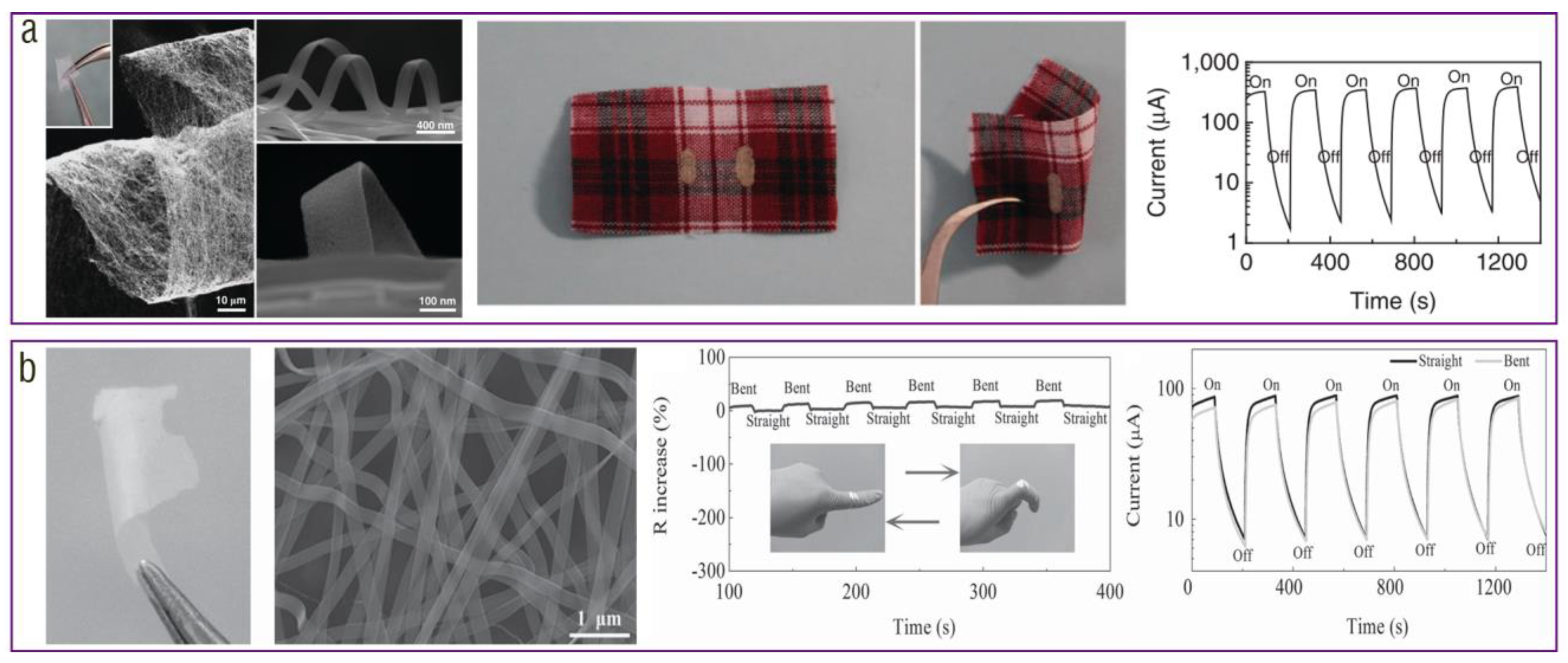
4.1. Wearable Electrospun Pressure Sensors

According to working mechanisms, current electrospun pressure sensors can be divided into capacitive, piezoresistive, piezoelectric, triboelectric, and iontronic pressure sensors [7,150,151]. Electrospun 1D fibrous, 2D interconnected network, and 2D aligned fiber structures are able to improve the stress distribution and enhance the stretchability of piezoelectric and piezoelectric strain sensors [104,152]. For example, Huang et al. prepared a 1D serpentine self-similar electrospun PVDF piezoelectric fiber array—which, serving as a piezoelectric velocity, strain, and pressure sensor—possessed a high stretchability of more than 300% [153]. This piezoelectric sensor was able to monitor posture and movement of the human body for healthcare. The network and porous structures in the interiors of 2D and 3D electrospun mats could provide good compressibility and associated electrostatic effect, which were beneficial for enhancing the capacitance, resistance, and voltage changes of capacitive, piezoresistive, and triboelectric pressure sensors under a certain pressure [154,155]. For example, Zhang et al. fabricated a triboelectric action sensor consisting of electrospun nanoporous fibers, which delivered ultrahigh electrical outputs of 56.9 W m−2 and 2209 V under an impact force of 100 N. Owing to its excellent electrical performances and, therefore, high signal-to-noise ratio, the triboelectric sensor was able to detect various body motions, such as running, walking, and picking up an object [37]. Some 3D (secondary) microstructures or 3D gradient microarrays on the electrospun mat surface were able to improve the effective contact area, stress distribution, and compressibility of triboelectric, iontronic, piezoresistive, piezoelectric, and capacitive pressure sensors at a certain pressure [1,135,156]. The 3D spiral structure of the electrospun yarn enhanced the stretchability and strength of the piezoresistive strain sensors [130]. These inherent structural advantages of electrospun fibers and fabrics optimize multiple sensing properties, especially sensitivity and detection limit, of corresponding wearable sensors and, therefore, promote their application in health, action, and manipulation monitoring [7]. Additionally, optimizing electrospun fiber density and alignment can further endow these wearable devices with new functions and better usage experience. For example, Yang et al. used a pair of 2D uniaxially aligned antimony-doped tin oxide electrospun nanofiber films to assemble a wearable strain sensor with direction-awareness and high transparency (Figure 8a) [157]. The single electrospun film exhibited exceptional anisotropic sensing performance, allowing for unidirectional sensing capability along the nanofiber direction. This sensing property was leveraged to construct the direction-aware biaxial strain sensor by stacking these two electrospun films orthogonally. Meanwhile, they demonstrated the potential of this direction-aware strain sensor for multi-degree-of-freedom applications, such as human motion monitoring and human–machine interaction. In addition, Zhang et al. used ultrathin, ultralight, gas-permeable 3D EMPA films to design a capacitive–triboelectric hybrid sensor with high sensitivity of 19 kPa−1, ultralow detection limit of 0.05 Pa, ultrafast response less than 0.8 ms, and good imperceptibility (Figure 6z) [1]. This on-skin sensor could detect an ultraweak fingertip pulse during monitoring of natural finger manipulation over a wide frequency range with minimal sensory interference, which was suitable for recording complicated manipulation details and detecting mental stress and emotion information of the eSports players (Figure 8b).

4.2. Wearable Electrospun Temperature Sensors

Temperature is a fundamental physical indicator that reflects the human physiological, psychological, and health status. The human body temperature is approximately 36–37 °C, and the pleasant ambient temperature is usually between 18 and 24 °C. Deviations from this range, whether too high or too low, can cause certain harm to human health. In addition, the ambient temperature can also affect people’s comfort levels. Wearable electrospun temperature sensors can be divided mainly into thermochromic and resistive temperature sensors [158,159,160,161]. Thermochromic sensors render an effective and intuitive real-time solution to detect the local temperature by the naked eye. In general, electrospun thermochromic temperature sensors are prepared by adding colorimetric dyes to the liquid precursor with a subsequent electrospinning process. Compared with traditional dense film-based thermochromic sensors exposing many dye molecules to the surface, the porous electrospun nanofiber structure with uniformly distributed dyes possesses superior light transmittance and, therefore, higher sensitivity and faster response speed. Kim et al. prepared an electrospun thermochromic sensor using (C3H6N6·CH2O)x as thermochromic dyes, which had high sensitivity and fast response time at 31.6–42.7 °C (Figure 9a). They found that the aligned electrospun nanofiber-based sensor showed 1.67-fold enhancement in thermochromic sensing performances compared with a randomly oriented fiber sensor (Figure 9b). Moreover, the electrospun thermochromic fibers can be processed into 2D films and 3D yarns to monitor real-time body temperature in the forms of patches, masks, and bracelets (Figure 9c) [158].
In terms of the electrospun resistive temperature sensor, it is usually integrated with the electrospun pressure/strain sensor, achieving dual-function sensing [159,160,161]. The current key points for this type of dual-function sensors are pressure–temperature signal decoupling and sensing performance enhancement, including sensitivity and response time. Wang et al. prepared 2D electrospun thermoplastic polyurethane (TPU) films and integrated resistive-temperature- and capacitive-pressure-sensing units to the electrospun TPU films, forming an all-fiber fully decoupled dual-function sensor with other advantages of air permeability, humidity inertness, and waterproof ability (Figure 9a) [160]. The resistive temperature sensor layer comprised a serpentine poly(3,4-ethylenedioxythiophene):poly(styrenesulfonate) (PEDOT:PSS)/PVA/G layer on top of two PEDOT:PSS interdigital electrodes. The capacitive pressure sensor layer was an ionic liquid/TPU fabric electrolyte layer on top of the supercapacitive PEDOT:PSS/PVA/Co3O4 interdigital electrodes. Since the temperature and pressure sensing units were based on completely different mechanisms, dual signals were successfully decoupled. The temperature change of 0.1 °C resulted in a fast response time of 0.7 s. Meanwhile, the temperature and pressure sensitivities reached up to 0.040 °C−1 and 147.19 kPa−1, respectively. On the basis of these merits, this wearable sensor was capable of monitoring pulse beats and body temperature at the wrist before and after exercise in a wireless and real-time mode [160].

4.3. Wearable Electrospun Gas Sensors

Toxic and harmful gases in the air affect the health of people. The exhaled gases reflect the health status of the body. The timely detection of gases can provide a good understanding of the state of health and air pollution, which is of great importance for disease prevention, early treatment, and human health protection [162]. The large specific surface area and high porosity of electrospun fabrics render numerous active sites to connect with gas molecules, which have huge potential to achieve rapid gas sensing [26]. Common wearable electrospun gas sensors can be divided into chemical dye, resistive, and triboelectric gas sensors [13,163]. Electrospun chemical dye gas sensors as a visible sensing technology allow people to directly identify targeted analytes with their eyes [163]. Kim et al. embedded ion-pairing dyes into stacked nanofibers via electrospinning, realizing harmful-gas sensors with sub-ppm theoretical detection limits (e.g., 0.15 ppm for formaldehyde) (Figure 10a) [13]. The dye-based electrospun sensing array comprised 12 sensing elements with varying initial states. Due to the wide range of color variations available with these dyes, the resulting color map generated by the array was both uncomplicated and accurate enough to differentiate among functional groups, such as amines, aldehydes, and carboxylic acids, as well as varying carbon chain lengths. Utilizing these nanofiber mats, an optoelectronic filter system could be implemented to detect formaldehyde in the surrounding area and to verify the successful elimination of the detected formaldehyde through the gas filter cartridge [13]. Electrospun resistive gas sensors have been widely studied. Zhang et al. prepared uniaxially aligned and randomly oriented electrospun PEDOT:PSS/PVP composite nanofibers as a resistive gas sensor to detect carbon monoxide (CO), and a linear relationship was observed between the response of PEDOT:PSS nanofibers and the concentration of CO within the range of 5–50 ppm (Figure 10b) [33]. Electrospun triboelectric gas sensors are based on changes in electrical signals caused by changes in properties, such as the dielectric constant, due to adsorption of gas molecules by tribo-materials [164]. In addition, triboelectric gas sensors can achieve self-powered sensing [165].

4.4. Wearable Electrospun Humidity Sensors

The measurement and control of local humidity are of great importance for improving the quality of human life. The large specific surface area and high porosity of electrospun fabrics are also beneficial for humidity sensing. There are four common types of wearable electrospun humidity sensors, including resistive, capacitive, colorimetric, and triboelectric humidity sensors [14,166,167,168]. For example, You et al. prepared electrospun 2D composite nanofibrous films composed of polyamide 66 and cobalt chloride (PA66/CoCl2), which were used as colorimetric humidity sensors [169]. The sensors displayed a noticeable color transformation from blue to pink as the relative humidity increased from 12.4 to 97.2%, attributed to the color-changing properties of CoCl2 (Figure 11a). Moreover, the fabricated sensors demonstrated desirable features, such as fast response and recovery time (less than 65.4 s and 11 s), low hysteresis (less than 11%), excellent reproducibility, and stability [169]. Recently, the wearable electrospun humidity sensors based on some new mechanisms were developed. Su et al. proposed a sensing-transducing coupled piezoelectric strategy by integrating a high-piezoresponse ceramic into a moisture-sensitive polyetherimide (PEI) polymer matrix through electrospinning [170]. This technique allowed for simultaneous and synchronous humidity perception and signal transduction and achieved a high sensitivity of 0.9% per relative humidity and a fast response time of 20 s to ambient moisture (Figure 11b). This sensor was designed to adhere to the skin, allowing for simultaneous monitoring of tension and the level of sweat on the skin [170].

4.5. Wearable Electrospun Biomolecule Sensors

The biomolecules in the human body reflect the state of physical health, and detecting these molecules can provide valuable insights into the body’s condition. This is particularly important for preventing the spread of infectious diseases and early treatment of major chronic illnesses. It should be noted that human biomolecules may contain various components, such as bacteria and viruses, and effective methods are needed to detect them [171]. Electrospun polymeric nanofiber membranes can be easily modified and functionalized with more target binding sites and sensing elements to improve their sensitivity and selectivity for biomolecule analytes [172]. For example, Frias et al. produced an asymmetrical nanofiber-based mat with an open-porous characteristic by the electrospinning of PVA and alginated polymers and posterior hierarchization with conductive polyaniline, which was used to detect the Zika virus (Figure 12) [173].

4.6. Wearable Electrospun Photosensors

Wearable photosensors have the potential to improve human health and life in several ways, such as monitoring UV radiation exposure, detecting glucose levels in individuals with diabetes, drug development, and personalized medicine [27]. Currently, wearable electrospun photosensors featuring low-dimensional nanostructures are used mainly to monitor UV radiation exposure. Excessive exposure to UV radiation can cause skin damage and increase the risk of skin cancer. By monitoring UV radiation exposure in real-time, wearable electrospun photosensors can help individuals to take steps to reduce their risk of skin damage and cancer. For example, Huang et al. utilized highly flexible ceramic nanobelts to construct a suitable “invisible” soft UV photodetector (Figure 13a) [174]. The remarkable mechanical flexibility and optical transparency of the nanobelt network could be attributed to its tightly entangled network structure and customized ribbon geometry. Despite being bent to a radius of 1 mm, the conductivity of the SnO2 nanobelt remained stable during the bending process. Even after 1000 cycles of bending to a radius of 2 mm, the resistance of the nanobelt network increased by only 110%. This nanobelt network could be conveniently and effectively transferred to or integrated with any functional electronic device, and its flexibility or stretchability could be modified on the basis of the surface structure of different substrates, allowing for the selection of appropriately flexible or curved substrates for the preparation of “invisible” UV photodetectors at a low cost [174]. In addition, they also fabricated a wearable electrospun photosensor based on SnO2 nanobelts, which was able to maintain consistent performance even when subjected to finger bending (Figure 13b) [175]. This is because the inorganic SnO2 nanobelt network featured a buckling open-mesh configuration, high optical transparency (>86% at 550 nm), and remarkable stretchability (≈160%). The light-switching process of this sensor displayed a nearly constant light-response performance and recovery speed. These nanobelts could be laminated onto various surfaces to create wearable UV photodetectors that demonstrated reliable photoelectric performance and were able to tolerate repeated complex deformations caused by human movement [175].

5. Conclusions and Outlook

This review begins with a description of the principle, typical apparatuses (including NFES, SDES, and FFES), and key components (including high-voltage power supply, spinneret, and collector) of electrospinning for producing wearable sensors. Then, we elaborate on construction strategies and physical properties of microstructured functional electrospun fabrics for wearable sensing. In the section of construction strategies, we discuss mainly how to construct various typical 1D, 2D, and 3D electrospun microstructures by NFES, SDES, and FFES. In the section on physical properties, breathability, imperceptibility, thermal–moisture stability, flexibility, stretchability, transparency, and robustness of wearable electrospun sensing textiles are mainly discussed. Subsequently, we review the applications of various 1D, 2D, and 3D microstructured electrospun textiles in sensing pressure, temperature, gas, humidity, biochemical molecules, and light for physiological signal recognition, behavior monitoring, personal protection, and health diagnosis. Finally, we summarize the challenges of constructing functional electrospun microstructures of wearable sensors for physiological signal detection and healthcare as follows:
  • It was demonstrated that constructing complex microstructures usually endows the wearable devices with superior sensing performances. Currently, a majority of classic functional microstructures, such as micropyramid, microcone, microhelix, and thin-layer structures, are created by photolithography, 3D printing, hydrothermal synthesis, inkjet printing, and screen printing. Photolithography and 3D printing can produce very regular and highly designable microstructures. Both techniques are suitable for directly processing a wide range of materials, such as inorganic crystals and organic polymers, without the requirement of complicated process exploration. According to the growth law of crystals, hydrothermal synthesis can also yield highly regular microstructures with material and geometric specificities. Inkjet printing and screen printing can produce precise thin-layer patterns with ultrahigh resolution and controllable thickness ranging from a few nanometers to tens of microns. In contrast to the above five classic processing technologies, it is difficult to obtain highly regular microstructures through electrospinning, which hinders the study of rigorous structure–performance relationships for electrospun functional microstructures, especially for sophisticated electrospun microstructures. Moreover, compared with photolithography and 3D printing, complicated process exploration, in general, is needed for expanding a certain sophisticated electrospun microstructure to new material systems. For example, our group developed a self-assembly strategy to create the electrospun micropyramid array. We spent much effort to endow various polymer materials with this type of advanced electrospun microstructure [1]. In addition, electrospinning requires liquid precursors and cannot directly process solid materials, which further limits its material universality compared with photolithography and 3D printing. Therefore, we should develop systematic strategies and easy-to-implement methods to promote the material universality and improve the geometrical regularity of sophisticated electrospun microstructures, widening their functionality as much as possible. Furthermore, we should develop various classic high-performance microstructures by electrospinning as well as guarantee the inherent merits, such as high gas-permeability, porosity, and specific surface area, of electrospun products to further improve the sensing performances, comfort, and practicality of wearable devices. Over the past several years, our group has developed various complex self-assembled electrospun microstructures (secondary micro-nanospheres [5], hierarchical micropapillaries [3], gradient micropores [2], micropyramid arrays [1], etc.) for high-performance comfortable sensors, which may inspire the design and preparation of new functional electrospun microstructures.
  • The special and attractive phenomenon in FFES is the self-assembly of regular microstructure. Meanwhile, the classic self-assembled electrospun microstructures (e.g., interconnected 2D nano-nets and 3D micro-honeycombs) have huge potential in achieving advanced wearable sensors. However, the electrospinning self-assembly mechanisms of these microstructures are still not very clear [176,177]. More attention should be paid to investigate explicit self-assembly mechanisms for developing more suitable electrospun microstructures in the field of wearable sensing.
  • In the past, the development of electrospun sensors focused only on their network structures that produced good permeability, large specific surface area, and numerous functional sites. Recently, Someya’s group exploited the attractive imperceptibility of ultrathin, ultralight, gas-permeable electrospun sensors, which triggered new application prospects of wearable pressure sensors in clinical restoration of hand function and digital archiving of a craftsperson’s skills [29]. Therefore, focusing on the specificities of existing electrospun microstructures, we should further expand and deepen their applications in wearable sensing.
  • At present, it is difficult for wearable electrospun sensors to integrate biophysical, electrical, optical, and biochemical sensing modalities together, hindering the sensing capabilities and often leading to expensive products. It is imperative to integrate multiple sensing modalities onto a single platform to enhance health monitoring efficiency and level. This will enable the measurement of more selective and specific bio-signals, allowing for a comprehensive evaluation of health conditions and body statuses.

Author Contributions

Conceptualization, J.-H.Z.; writing—original draft preparation, J.-H.Z.; writing—review and editing, J.-H.Z., L.P., Y.S., X.S., H.W., J.L., X.G., Y.W., W.C., H.Q. and S.L.; supervision, L.P. and Y.S. All authors have read and agreed to the published version of the manuscript.

Funding

This research was funded by the National Key Research and Development program of China grant number [2021YFA1401103], the Natural Science Foundation of China [61825403 and 61921005], and the Postgraduate Research & Practice Innovation Program of Jiangsu Province.

Acknowledgments

We appreciate the help and cordial discussions from Qiang Tang (ORCID: 0000-0003-0360-5526), Zhengtong Li (ORCID: 0000-0002-4916-0924), and Feiyu Wang.

Conflicts of Interest

The authors declare no conflict of interest.

References

  1. Zhang, J.-H.; Li, Z.; Xu, J.; Li, J.; Yan, K.; Cheng, W.; Xin, M.; Zhu, T.; Du, J.; Chen, S.; et al. Versatile self-assembled electrospun micropyramid arrays for high-performance on-skin devices with minimal sensory interference. Nat. Commun. 2022, 13, 5839. [Google Scholar] [CrossRef] [PubMed]
  2. Zhang, J.-H.; Li, Y.; Du, J.; Hao, X.; Wang, Q. Bio-inspired hydrophobic/cancellous/hydrophilic Trimurti PVDF mat-based wearable triboelectric nanogenerator designed by self-assembly of electro-pore-creating. Nano Energy 2019, 61, 486–495. [Google Scholar] [CrossRef]
  3. Zhang, J.-H.; Hao, X. Enhancing Output Performances and Output Retention Rates of Triboelectric Nanogenerators via a Design of Composite Inner-Layers with Coupling Effect and Self-Assembled Outer-Layers with Superhydrophobicity. Nano Energy 2020, 76, 105074. [Google Scholar] [CrossRef]
  4. Zhang, J.-H.; Zhang, Y.; Sun, N.; Li, Y.; Du, J.; Zhu, L.; Hao, X. Enhancing output performance of triboelectric nanogenerator via large polarization difference effect. Nano Energy 2021, 84, 105892. [Google Scholar] [CrossRef]
  5. Zhang, J.-H.; Li, Y.; Du, J.; Hao, X.; Huang, H. A high-power wearable triboelectric nanogenerator prepared from self-assembled electrospun poly(vinylidene fluoride) fibers with a heart-like structure. J. Mater. Chem. A 2019, 7, 11724–11733. [Google Scholar] [CrossRef]
  6. Zhang, J.-H.; Zhou, Z.; Li, J.; Shen, B.; Zhu, T.; Gao, X.; Tao, R.; Guo, X.; Hu, X.; Shi, Y.; et al. Coupling Enhanced Performance of Triboelectric–Piezoelectric Hybrid Nanogenerator Based on Nanoporous Film of Poly(vinylidene fluoride)/BaTiO3 Composite Electrospun Fibers. ACS Mater. Lett. 2022, 4, 847–852. [Google Scholar] [CrossRef]
  7. Heikenfeld, J.; Jajack, A.; Rogers, J.; Gutruf, P.; Tian, L.; Pan, T.; Li, R.; Khine, M.; Kim, J.; Wang, J.; et al. Wearable sensors: Modalities, challenges, and prospects. Lab Chip 2018, 18, 217–248. [Google Scholar] [CrossRef]
  8. Luo, Y.; Abidian, M.R.; Ahn, J.H.; Akinwande, D.; Andrews, A.M.; Antonietti, M.; Bao, Z.; Berggren, M.; Berkey, C.A.; Bettinger, C.J.; et al. Technology Roadmap for Flexible Sensors. ACS Nano 2023, 17, 5211–5295. [Google Scholar] [CrossRef]
  9. Sun, Y.; Li, J.; Li, S.; Jiang, Y.; Wan, E.; Zhang, J.-H.; Shi, Y.; Pan, L. Advanced synaptic devices and their applications in biomimetic sensory neural system. Chip 2023, 2, 100031. [Google Scholar] [CrossRef]
  10. Wan, B.; Dong, X.; Yang, X.; Wang, J.; Zheng, M.S.; Dang, Z.M.; Chen, G.; Zha, J.W. Rising of Dynamic Polyimide Materials: A Versatile Dielectric for Electrical and Electronic Applications. Adv. Mater. 2023, 10, e2301185. [Google Scholar] [CrossRef]
  11. Ma, Z.; Kong, D.; Pan, L.; Bao, Z. Skin-inspired electronics: Emerging semiconductor devices and systems. J. Semicond. 2020, 41, 041601. [Google Scholar] [CrossRef]
  12. Zhou, Y.; Zhang, J.-H.; Li, S.; Qiu, H.; Shi, Y.; Pan, L. Triboelectric Nanogenerators Based on 2D Materials: From Materials and Devices to Applications. Micromachines 2023, 14, 1043. [Google Scholar] [CrossRef]
  13. Kim, D.; Hwang, K.S.; Koh, W.G.; Lee, C.; Lee, J.Y. Volatile Organic Compound Sensing Array and Optoelectronic Filter System using Ion-Pairing Dyes with a Wide Visible Spectrum. Adv. Mater. 2022, 34, e2203671. [Google Scholar] [CrossRef]
  14. Lai, Y.C.; Deng, J.; Liu, R.; Hsiao, Y.C.; Zhang, S.L.; Peng, W.; Wu, H.M.; Wang, X.; Wang, Z.L. Actively Perceiving and Responsive Soft Robots Enabled by Self-Powered, Highly Extensible, and Highly Sensitive Triboelectric Proximity- and Pressure-Sensing Skins. Adv. Mater. 2018, 30, e1801114. [Google Scholar] [CrossRef]
  15. Li, D.; Liu, X.; Li, W.; Lin, Z.; Zhu, B.; Li, Z.; Li, J.; Li, B.; Fan, S.; Xie, J.; et al. Scalable and hierarchically designed polymer film as a selective thermal emitter for high-performance all-day radiative cooling. Nat. Nanotechnol. 2021, 16, 153–158. [Google Scholar] [CrossRef]
  16. Chen, G.; Matsuhisa, N.; Liu, Z.; Qi, D.; Cai, P.; Jiang, Y.; Wan, C.; Cui, Y.; Leow, W.R.; Liu, Z.; et al. Plasticizing silk protein for on-skin stretchable electrodes. Adv. Mater. 2018, 30, e1800129. [Google Scholar] [CrossRef]
  17. Dong, K.; Peng, X.; Wang, Z.L. Fiber/Fabric-Based Piezoelectric and Triboelectric Nanogenerators for Flexible/Stretchable and Wearable Electronics and Artificial Intelligence. Adv. Mater. 2020, 32, e1902549. [Google Scholar] [CrossRef] [PubMed]
  18. Fan, W.; He, Q.; Meng, K.; Tan, X.; Zhou, Z.; Zhang, G.; Yang, J.; Wang, Z.L. Machine-knitted washable sensor array textile for precise epidermal physiological signal monitoring. Sci. Adv. 2020, 6, eaay2840. [Google Scholar] [CrossRef] [PubMed]
  19. Ouyang, H.; Tian, J.; Sun, G.; Zou, Y.; Liu, Z.; Li, H.; Zhao, L.; Shi, B.; Fan, Y.; Fan, Y.; et al. Self-Powered Pulse Sensor for Antidiastole of Cardiovascular Disease. Adv. Mater. 2017, 29, 1703456. [Google Scholar] [CrossRef]
  20. Bai, Z.; Xu, Y.; Li, J.; Zhu, J.; Gao, C.; Zhang, Y.; Wang, J.; Guo, J. An Eco-friendly Porous Nanocomposite Fabric-Based Triboelectric Nanogenerator for Efficient Energy Harvesting and Motion Sensing. ACS Appl. Mater. Interfaces 2020, 12, 42880–42890. [Google Scholar] [CrossRef]
  21. Niu, S.; Wang, X.; Yi, F.; Zhou, Y.S.; Wang, Z.L. A universal self-charging system driven by random biomechanical energy for sustainable operation of mobile electronics. Nat. Commun. 2015, 6, 8975. [Google Scholar] [CrossRef]
  22. Kaltenbrunner, M.; Sekitani, T.; Reeder, J.; Yokota, T.; Kuribara, K.; Tokuhara, T.; Drack, M.; Schwodiauer, R.; Graz, I.; Bauer-Gogonea, S.; et al. An ultra-lightweight design for imperceptible plastic electronics. Nature 2013, 499, 458–463. [Google Scholar] [CrossRef] [PubMed]
  23. Zhu, M.; Shi, Q.; He, T.; Yi, Z.; Ma, Y.; Yang, B.; Chen, T.; Lee, C. Self-Powered and Self-Functional Cotton Sock Using Piezoelectric and Triboelectric Hybrid Mechanism for Healthcare and Sports Monitoring. ACS Nano. 2019, 13, 1940–1952. [Google Scholar] [CrossRef] [PubMed]
  24. Miyamoto, A.; Lee, S.; Cooray, N.F.; Lee, S.; Mori, M.; Matsuhisa, N.; Jin, H.; Yoda, L.; Yokota, T.; Itoh, A.; et al. Inflammation-free, gas-permeable, lightweight, stretchable on-skin electronics with nanomeshes. Nat. Nanotechnol. 2017, 12, 907–913. [Google Scholar] [CrossRef] [PubMed]
  25. Wang, H.; Kurokawa, Y.; Gotoh, K.; Kato, S.; Yamada, S.; Itoh, T.; Usami, N. Performance enhancement of droplet-based electricity generator using a CYTOP intermediate layer. Jpn. J. Appl. Phys. 2023, 62, SC1032. [Google Scholar] [CrossRef]
  26. Song, J.; Lin, X.; Ee, L.Y.; Li, S.F.Y.; Huang, M. A Review on Electrospinning as Versatile Supports for Diverse Nanofibers and Their Applications in Environmental Sensing. Adv. Fiber. Mater. 2022, 5, 429–460. [Google Scholar] [CrossRef]
  27. Wang, Y.; Wu, H.; Lin, D.; Zhang, R.; Li, H.; Zhang, W.; Liu, W.; Huang, S.; Yao, L.; Cheng, J.; et al. One-dimensional electrospun ceramic nanomaterials and their sensing applications. J. Am. Ceram. Soc. 2021, 105, 765–785. [Google Scholar] [CrossRef]
  28. Xue, J.; Wu, T.; Dai, Y.; Xia, Y. Electrospinning and Electrospun Nanofibers: Methods, Materials, and Applications. Chem. Rev. 2019, 119, 5298–5415. [Google Scholar] [CrossRef]
  29. Lee, S.; Franklin, S.; Hassani, F.A.; Yokota, T.; Nayeem, M.O.G.; Wang, Y.; Leib, R.; Cheng, G.; Franklin, D.W.; Someya, T. Nanomesh pressure sensor for monitoring finger manipulation without sensory interference. Science 2020, 370, 966–970. [Google Scholar] [CrossRef]
  30. Wang, Y.; Lee, S.; Wang, H.; Jiang, Z.; Jimbo, Y.; Wang, C.; Wang, B.; Kim, J.J.; Koizumi, M.; Yokota, T.; et al. Robust, self-adhesive, reinforced polymeric nanofilms enabling gas-permeable dry electrodes for long-term application. Proc. Natl. Acad. Sci. USA 2021, 118, e2111904118. [Google Scholar] [CrossRef]
  31. Wang, X.; Dong, L.; Zhang, H.; Yu, R.; Pan, C.; Wang, Z.L. Recent progress in electronic skin. Adv. Sci. 2015, 2, 1500169. [Google Scholar] [CrossRef] [PubMed]
  32. Ahirwal, D.; Hébraud, A.; Kádár, R.; Wilhelm, M.; Schlatter, G. From self-assembly of electrospun nanofibers to 3D cm thick hierarchical foams. Soft Matter 2013, 9, 3164–3172. [Google Scholar] [CrossRef]
  33. Zhang, H.-D.; Yan, X.; Zhang, Z.-H.; Yu, G.-F.; Han, W.-P.; Zhang, J.-C.; Long, Y.-Z. Electrospun PEDOT:PSS/PVP Nanofibers for CO Gas Sensing with Quartz Crystal Microbalance Technique. Int. J. Polym. Sci. 2016, 2016, 3021353. [Google Scholar] [CrossRef]
  34. Yu, H.; Huang, T.; Lu, M.; Mao, M.; Zhang, Q.; Wang, H. Enhanced power output of an electrospun PVDF/MWCNTs-based nanogenerator by tuning its conductivity. Nanotechnology 2013, 24, 405401. [Google Scholar] [CrossRef] [PubMed]
  35. Luo, C.J.; Stoyanov, S.D.; Stride, E.; Pelan, E.; Edirisinghe, M. Electrospinning versus fibre production methods: From specifics to technological convergence. Chem. Soc. Rev. 2012, 41, 4708–4735. [Google Scholar] [CrossRef] [PubMed]
  36. Li, D.; Xia, Y. Electrospinning of Nanofibers: Reinventing the Wheel? Adv. Mater. 2004, 16, 1151–1170. [Google Scholar] [CrossRef]
  37. Zhang, D.; Chang, J. Electrospinning of three-dimensional nanofibrous tubes with controllable architectures. Nano Lett. 2008, 8, 3283–3287. [Google Scholar] [CrossRef]
  38. Li, D.; Wang, Y.; Xia, Y. Electrospinning of polymeric and ceramic nanofibers as uniaxially aligned arrays. Nano Lett. 2003, 3, 1167–1171. [Google Scholar] [CrossRef]
  39. Zhang, J.-H.; Li, Y.; Hao, X. A high-performance triboelectric nanogenerator with improved output stability by construction of biomimetic superhydrophobic nanoporous fibers. Nanotechnology 2020, 31, 215401. [Google Scholar] [CrossRef]
  40. Zhang, S.; Liu, H.; Tang, N.; Ge, J.; Yu, J.; Ding, B. Direct electronetting of high-performance membranes based on self-assembled 2D nanoarchitectured networks. Nat. Commun. 2019, 10, 1458. [Google Scholar] [CrossRef]
  41. Wan, C.; Bowen, C.R. Multiscale-structuring of polyvinylidene fluoride for energy harvesting: The impact of molecular-, micro- and macro-structure. J. Mater. Chem. A 2017, 5, 3091–3128. [Google Scholar] [CrossRef]
  42. Sun, B.; Long, Y.Z.; Yu, F.; Li, M.M.; Zhang, H.D.; Li, W.J.; Xu, T.X. Self-assembly of a three-dimensional fibrous polymer sponge by electrospinning. Nanoscale 2012, 4, 2134–2137. [Google Scholar] [CrossRef] [PubMed]
  43. Reis, T.C.; Correia, I.J.; Aguiar-Ricardo, A. Electrodynamic tailoring of self-assembled three-dimensional electrospun constructs. Nanoscale 2013, 5, 7528–7536. [Google Scholar] [CrossRef] [PubMed]
  44. Yu, X.; Li, Y.; Wang, X.; Si, Y.; Yu, J.; Ding, B. Thermoconductive, moisture-permeable, and superhydrophobic nanofibrous membranes with interpenetrated boron nitride network for personal cooling fabrics. ACS Appl. Mater. Interfaces 2020, 12, 32078–32089. [Google Scholar] [CrossRef]
  45. Wang, X.-X.; Yu, G.-F.; Zhang, J.; Yu, M.; Ramakrishna, S.; Long, Y.-Z. Conductive polymer ultrafine fibers via electrospinning: Preparation, physical properties and applications. Prog. Mater. Sci. 2021, 115, 100704. [Google Scholar] [CrossRef]
  46. Thandavamoorthy, S.; Gopinath, N.; Ramkumar, S.S. Self-assembled honeycomb polyurethane nanofibers. J. Appl. Polym. Sci. 2006, 101, 3121–3124. [Google Scholar] [CrossRef]
  47. Sun, D.; Chang, C.; Li, S.; Lin, L. Near-Field Electrospinning. Nano Lett. 2006, 6, 839–842. [Google Scholar] [CrossRef]
  48. Persano, L.; Dagdeviren, C.; Su, Y.; Zhang, Y.; Girardo, S.; Pisignano, D.; Huang, Y.; Rogers, J.A. High performance piezoelectric devices based on aligned arrays of nanofibers of poly(vinylidenefluoride-co-trifluoroethylene). Nat. Commun. 2013, 4, 1633. [Google Scholar] [CrossRef]
  49. Lee, S.; Sasaki, D.; Kim, D.; Mori, M.; Yokota, T.; Lee, H.; Park, S.; Fukuda, K.; Sekino, M.; Matsuura, K.; et al. Ultrasoft electronics to monitor dynamically pulsing cardiomyocytes. Nat. Nanotechnol. 2018, 14, 156–160. [Google Scholar] [CrossRef]
  50. Fang, J.; Niu, H.; Wang, H.; Wang, X.; Lin, T. Enhanced mechanical energy harvesting using needleless electrospun poly(vinylidene fluoride) nanofibre webs. Energy Environ. Sci. 2013, 6, 2196–2202. [Google Scholar] [CrossRef]
  51. Lee, C.; Wood, D.; Edmondson, D.; Yao, D.; Erickson, A.E.; Tsao, C.T.; Revia, R.A.; Kim, H.; Zhang, M. Electrospun uniaxially-aligned composite nanofibers as highly-efficient piezoelectric material. Ceram. Int. 2016, 42, 2734–2740. [Google Scholar] [CrossRef]
  52. Guo, Y.; Zhang, X.-S.; Wang, Y.; Gong, W.; Zhang, Q.; Wang, H.; Brugger, J. All-fiber hybrid piezoelectric-enhanced triboelectric nanogenerator for wearable gesture monitoring. Nano Energy 2018, 48, 152–160. [Google Scholar] [CrossRef]
  53. Wan, Y.; Qiu, Z.; Hong, Y.; Wang, Y.; Zhang, J.; Liu, Q.; Wu, Z.; Guo, C.F. A Highly Sensitive Flexible Capacitive Tactile Sensor with Sparse and High-Aspect-Ratio Microstructures. Adv. Electron. Mater. 2018, 4, 1700586. [Google Scholar] [CrossRef]
  54. Nayeem, M.O.G.; Lee, S.; Jin, H.; Matsuhisa, N.; Jinno, H.; Miyamoto, A.; Yokota, T.; Someya, T. All-nanofiber-based, ultrasensitive, gas-permeable mechanoacoustic sensors for continuous long-term heart monitoring. Proc. Natl. Acad. Sci. USA 2020, 117, 7063–7070. [Google Scholar] [CrossRef]
  55. Hohman, M.M.; Shin, M.; Rutledge, G.; Brenner, M.P. Electrospinning and electrically forced jets. I. Stability theory. Phys. Fluids 2001, 13, 2201–2220. [Google Scholar] [CrossRef]
  56. Huang, Y.; Bu, N.; Duan, Y.; Pan, Y.; Liu, H.; Yin, Z.; Xiong, Y. Electrohydrodynamic direct-writing. Nanoscale 2013, 5, 12007–12017. [Google Scholar] [CrossRef]
  57. Shao, H.; Fang, J.; Wang, H.; Lang, C.; Lin, T. Robust Mechanical-to-Electrical Energy Conversion from Short-Distance Electrospun Poly(vinylidene fluoride) Fiber Webs. ACS Appl. Mater. Interfaces 2015, 7, 22551–22557. [Google Scholar] [CrossRef]
  58. Han, T.; Reneker, D.H.; Yarin, A.L. Buckling of jets in electrospinning. Polymer 2007, 48, 6064–6076. [Google Scholar] [CrossRef]
  59. Liashenko, I.; Rosell-Llompart, J.; Cabot, A. Ultrafast 3D printing with submicrometer features using electrostatic jet deflection. Nat. Commun. 2020, 11, 753. [Google Scholar] [CrossRef]
  60. Hu, X.; Yan, X.; Gong, L.; Wang, F.; Xu, Y.; Feng, L.; Zhang, D.; Jiang, Y. Improved Piezoelectric Sensing Performance of P(VDF-TrFE) Nanofibers by Utilizing BTO Nanoparticles and Penetrated Electrodes. ACS Appl. Mater. Interfaces 2019, 11, 7379–7386. [Google Scholar] [CrossRef]
  61. Nguyen, D.-N.; Hwang, Y.; Moon, W. Electrospinning of well-aligned fiber bundles using an End-point Control Assembly method. Eur. Polym. J. 2016, 77, 54–64. [Google Scholar] [CrossRef]
  62. Wang, H.; Sakamoto, H.; Asai, H.; Zhang, J.-H.; Meboso, T.; Uchiyama, Y.; Kobayashi, E.; Takamura, E.; Suye, S.-i. An all-fibrous triboelectric nanogenerator with enhanced outputs depended on the polystyrene charge storage layer. Nano Energy 2021, 90, 106515. [Google Scholar] [CrossRef]
  63. Guo, X.; Li, J.; Wang, F.; Zhang, J.-H.; Zhang, J.; Shi, Y.; Pan, L. Application of conductive polymer hydrogels in flexible electronics. J. Polym. Sci. 2022, 60, 2635–2662. [Google Scholar] [CrossRef]
  64. Zheng, J.-Y.; Liu, H.-Y.; Wang, X.; Zhao, Y.; Huang, W.-W.; Zheng, G.-F.; Sun, D.-H. Electrohydrodynamic Direct-Write Orderly Micro/Nanofibrous Structure on Flexible Insulating Substrate. J. Nanomater. 2014, 2014, 1–7. [Google Scholar] [CrossRef]
  65. Wang, P.; Liu, J.; Li, Y.; Li, G.; Yu, W.; Zhang, Y.; Meng, C.; Guo, S. Recent Advances in Wearable Tactile Sensors Based on Electrospun Nanofiber Platform. Adv. Sens. Res. 2023, 2, 2200047. [Google Scholar] [CrossRef]
  66. Zou, F.; Li, G.; Wang, X.; Yarin, A.L. Dynamic hydrophobicity of superhydrophobic PTFE-SiO2 electrospun fibrous membranes. J. Membr. Sci. 2021, 619, 118810. [Google Scholar] [CrossRef]
  67. Yang, G.; Li, X.; He, Y.; Ma, J.; Ni, G.; Zhou, S. From nano to micro to macro: Electrospun hierarchically structured polymeric fibers for biomedical applications. Prog. Polym. Sci. 2018, 81, 80–113. [Google Scholar] [CrossRef]
  68. Kessick, R.; Fenn, J.; Tepper, G. The use of AC potentials in electrospraying and electrospinning processes. Polymer 2004, 45, 2981–2984. [Google Scholar] [CrossRef]
  69. You, S.; Zhang, L.; Gui, J.; Cui, H.; Guo, S. A Flexible Piezoelectric Nanogenerator Based on Aligned P(VDF-TrFE) Nanofibers. Micromachines 2019, 10, 302. [Google Scholar] [CrossRef]
  70. Liu, Q.; Zhu, J.; Zhang, L.; Qiu, Y. Recent advances in energy materials by electrospinning. Renew. Sustain. Energy Rev. 2018, 81, 1825–1858. [Google Scholar] [CrossRef]
  71. Jiang, G.; Qin, X. An improved free surface electrospinning for high throughput manufacturing of core–shell nanofibers. Mater. Lett. 2014, 128, 259–262. [Google Scholar] [CrossRef]
  72. Niu, H.; Lin, T.; Wang, X. Needleless electrospinning. I. A comparison of cylinder and disk nozzles. J. Appl. Polym. Sci. 2009, 114, 3524–3530. [Google Scholar] [CrossRef]
  73. Yang, R.; He, J.; Xu, L.; Yu, J. Bubble-electrospinning for fabricating nanofibers. Polymer 2009, 50, 5846–5850. [Google Scholar] [CrossRef]
  74. Wang, X.; Niu, H.; Wang, X.; Lin, T. Needleless Electrospinning of Uniform Nanofibers Using Spiral Coil Spinnerets. J. Nanomater. 2012, 2012, 1–9. [Google Scholar] [CrossRef]
  75. Niu, H.; Wang, X.; Lin, T. Needleless electrospinning: Influences of fibre generator geometry. J. Text. Inst. 2012, 103, 787–794. [Google Scholar] [CrossRef]
  76. Bhattacharyya, I.; Molaro, M.C.; Braatz, R.D.; Rutledge, G.C. Free surface electrospinning of aqueous polymer solutions from a wire electrode. Chem. Eng. J. 2016, 289, 203–211. [Google Scholar] [CrossRef]
  77. Zheng, Y.; Gong, R.H.; Zeng, Y. Multijet motion and deviation in electrospinning. RSC Adv. 2015, 5, 48533–48540. [Google Scholar] [CrossRef]
  78. SalehHudin, H.S.; Mohamad, E.N.; Mahadi, W.N.L.; Muhammad Afifi, A. Multiple-jet electrospinning methods for nanofiber processing: A review. Mater. Manuf. Process. 2017, 33, 479–498. [Google Scholar] [CrossRef]
  79. Theron, S.A.; Yarin, A.L.; Zussman, E.; Kroll, E. Multiple jets in electrospinning: Experiment and modeling. Polymer 2005, 46, 2889–2899. [Google Scholar] [CrossRef]
  80. Chen, H.; Wang, N.; Di, J.; Zhao, Y.; Song, Y.; Jiang, L. Nanowire-in-microtube structured core/shell fibers via multifluidic coaxial electrospinning. Langmuir 2010, 26, 11291–11296. [Google Scholar] [CrossRef]
  81. Li, D.; Xia, Y. Direct Fabrication of Composite and Ceramic Hollow Nanofibers by Electrospinning. Nano Lett. 2004, 4, 933–938. [Google Scholar] [CrossRef]
  82. Yu, B.; Yu, H.; Huang, T.; Wang, H.; Zhu, M. A biomimetic nanofiber-based triboelectric nanogenerator with an ultrahigh transfer charge density. Nano Energy 2018, 48, 464–470. [Google Scholar] [CrossRef]
  83. Han, D.; Steckl, A.J. Triaxial electrospun nanofiber membranes for controlled dual release of functional molecules. ACS Appl Mater Interfaces 2013, 5, 8241–8245. [Google Scholar] [CrossRef]
  84. Li, D.; McCann, J.T.; Xia, Y. Use of electrospinning to directly fabricate hollow nanofibers with functionalized inner and outer surfaces. Small 2005, 1, 83–86. [Google Scholar] [CrossRef] [PubMed]
  85. Wang, N.; Chen, H.; Lin, L.; Zhao, Y.; Cao, X.; Song, Y.; Jiang, L. Multicomponent Phase Change Microfibers Prepared by Temperature Control Multifluidic Electrospinning. Macromol. Rapid Commun. 2010, 31, 1622–1627. [Google Scholar] [CrossRef] [PubMed]
  86. Katta, P.; Alessandro, M.; Ramsier, R.D.; Chase, G.G. Continuous Electrospinning of Aligned Polymer Nanofibers onto a Wire Drum Collector. Nano Lett. 2004, 4, 2215–2218. [Google Scholar] [CrossRef]
  87. Zussman, E.; Theron, A.; Yarin, A.L. Formation of nanofiber crossbars in electrospinning. Appl. Phys. Lett. 2003, 82, 973–975. [Google Scholar] [CrossRef]
  88. Li, D.; Wang, Y.; Xia, Y. Electrospinning Nanofibers as Uniaxially Aligned Arrays and Layer-by-Layer Stacked Films. Adv. Mater. 2004, 16, 361–366. [Google Scholar] [CrossRef]
  89. Dalton, P.D.; Klee, D.; Möller, M. Electrospinning with dual collection rings. Polymer 2005, 46, 611–614. [Google Scholar] [CrossRef]
  90. Huang, Z.-M.; Zhang, Y.Z.; Kotaki, M.; Ramakrishna, S. A review on polymer nanofibers by electrospinning and their applications in nanocomposites. Compos. Sci. Technol. 2003, 63, 2223–2253. [Google Scholar] [CrossRef]
  91. Deitzel, J.M.; Kleinmeyer, J.; Hirvonen, J.K.; Beck, T.N.C. Controlled deposition of electrospun poly(ethylene oxide) fibers. Polymer 2001, 42, 8163–8170. [Google Scholar] [CrossRef]
  92. McCann, J.T.; Marquez, M.; Xia, Y. Highly porous fibers by electrospinning into a cryogenic liquid. J. Am. Chem. Soc. 2006, 128, 1436–1437. [Google Scholar] [CrossRef] [PubMed]
  93. Dong, R.-H.; Jia, Y.-X.; Qin, C.-C.; Zhan, L.; Yan, X.; Cui, L.; Zhou, Y.; Jiang, X.; Long, Y.-Z. In situ deposition of a personalized nanofibrous dressing via a handy electrospinning device for skin wound care. Nanoscale 2016, 8, 3482–3488. [Google Scholar] [CrossRef] [PubMed]
  94. Hejazi, F.; Mirzadeh, H.; Contessi, N.; Tanzi, M.C.; Fare, S. Novel class of collector in electrospinning device for the fabrication of 3D nanofibrous structure for large defect load-bearing tissue engineering application. J. Biomed Mater. Res. A 2017, 105, 1535–1548. [Google Scholar] [CrossRef] [PubMed]
  95. Xin, M.; Yu, T.; Jiang, Y.; Tao, R.; Li, J.; Ran, F.; Zhu, T.; Huang, J.; Zhang, J.; Zhang, J.-H.; et al. Multi-vital on-skin optoelectronic biosensor for assessing regional tissue hemodynamics. In SmartMat; John Wiley & Sons: Hoboken, NJ, USA, 2022. [Google Scholar] [CrossRef]
  96. An, X.; Liu, J.; Zhang, J.-H.; Huang, X.; Zhu, T.; Yan, H.; Jia, X.; Zhang, Q. A robust and self-healing elastomer achieved by a thio-β-diketone-Cu(ii) coordination and H-bonding dual crosslinked system. Mater. Chem. Front. 2022, 6, 1779–1787. [Google Scholar] [CrossRef]
  97. Ma, W.; Wu, H.; Cai, Y.; Yu, Z.; Wang, Y.; Zhang, J.-H.; Zhang, Q.; Jia, X. A Flexible Single-Ion Gel Electrolyte with a Multiscale Channel for the High-Performance Lithium Metal Batteries. ACS Mater. Lett. 2022, 4, 944–952. [Google Scholar] [CrossRef]
  98. Tang, Q.; Zhang, Z.; Zhang, J.-H.; Tang, F.; Wang, C.; Cui, X. Oscillatory Motion of Water Droplets Both in Oil and on Superhydrophobic Surface under Corona Discharge. Micromachines 2022, 13, 2229. [Google Scholar] [CrossRef]
  99. Zhang, J.; Li, J.; Cheng, W.; Zhang, J.-H.; Zhou, Z.; Sun, X.; Li, L.; Liang, J.-G.; Shi, Y.; Pan, L. Challenges in Materials and Devices of Electronic Skin. ACS Mater. Lett. 2022, 4, 577–599. [Google Scholar] [CrossRef]
  100. Ying, S.; Zhang, J.-H.; Yan, K.; Xin, M.; Zhang, J.; Li, S.; Liang, J.; Shi, Y.; Pan, L. Self-powered direct-current type pressure sensor by polypyrrole/metal Schottky junction. J. Phys. D Appl. Phys. 2021, 54, 424008. [Google Scholar] [CrossRef]
  101. Yan, K.-B.; Guo, G.-B.; Liu, J.-y.; Huang, Q.; Zhang, J.-H. Preparation and characterization of oil/water separation membranes via grafting methyl methacrylate onto poly(vinylidene fluoride). Acta Polym. Sin. 2016, 5, 659–666. [Google Scholar]
  102. Zhang, J.-H.; Guo, G.-B.; An, S.-L.; Hao, Y.; Zhang, D.; Yan, K.-B. Synthesis and Properties of Proton Exchange Membranes via Single-Step Grafting PSBMA onto PVDF Modified by TMAH. Acta Phys.-Chim. Sin. 2015, 31, 1905–1913. [Google Scholar] [CrossRef]
  103. Zhang, D.; Guo, G.-B.; Hao, Y.; An, S.-L.; Zhang, J.-H.; Yan, K.-B. Preparation and characterization of membranes synthesized via one-step grafting acrylamido-methyl propane sulfonic onto poly(vinylidene fluoride) modified by tetramethylammonium hydroxide. Polym. Mater. Sci. Eng. 2016, 32, 706–712. [Google Scholar] [CrossRef]
  104. Wang, Y.; Lee, S.; Yokota, T.; Wang, H.; Jiang, Z.; Wang, J.; Koizumi, M.; Someya, T. A durable nanomesh on-skin strain gauge for natural skin motion monitoring with minimum mechanical constraints. Sci. Adv. 2020, 6, eabb7043. [Google Scholar] [CrossRef] [PubMed]
  105. Chang, C.; Tran, V.H.; Wang, J.; Fuh, Y.K.; Lin, L. Direct-write piezoelectric polymeric nanogenerator with high energy conversion efficiency. Nano Lett. 2010, 10, 726–731. [Google Scholar] [CrossRef]
  106. Fuh, Y.K.; Ye, J.C.; Chen, P.C.; Ho, H.C.; Huang, Z.M. Hybrid Energy Harvester Consisting of Piezoelectric Fibers with Largely Enhanced 20 V for Wearable and Muscle-Driven Applications. ACS Appl Mater Interfaces 2015, 7, 16923–16931. [Google Scholar] [CrossRef]
  107. Hansen, B.J.; Liu, Y.; Yang, R.; Wang, Z.L. Hybrid nanogenerator for concurrently harvesting biomechanical and biochemical energy. ACS Nano 2010, 4, 3647–3652. [Google Scholar] [CrossRef]
  108. Brown, T.D.; Dalton, P.D.; Hutmacher, D.W. Direct writing by way of melt electrospinning. Adv. Mater. 2011, 23, 5651–5657. [Google Scholar] [CrossRef]
  109. Wu, H.; Kong, D.; Ruan, Z.; Hsu, P.C.; Wang, S.; Yu, Z.; Carney, T.J.; Hu, L.; Fan, S.; Cui, Y. A transparent electrode based on a metal nanotrough network. Nat. Nanotechnol. 2013, 8, 421–425. [Google Scholar] [CrossRef]
  110. Ni, J.; Lin, S.; Qin, Z.; Veysset, D.; Liu, X.; Sun, Y.; Hsieh, A.J.; Radovitzky, R.; Nelson, K.A.; Zhao, X. Strong fatigue-resistant nanofibrous hydrogels inspired by lobster underbelly. Matter 2021, 4, 1919–1934. [Google Scholar] [CrossRef]
  111. Zhang, S.; Liu, H.; Tang, N.; Zhou, S.; Yu, J.; Ding, B. Spider-Web-Inspired PM(0.3) Filters Based on Self-Sustained Electrostatic Nanostructured Networks. Adv. Mater. 2020, 32, e2002361. [Google Scholar] [CrossRef]
  112. Zhang, S.; Liu, H.; Yu, J.; Li, B.; Ding, B. Multi-functional flexible 2D carbon nanostructured networks. Nat. Commun. 2020, 11, 5134. [Google Scholar] [CrossRef] [PubMed]
  113. Nazemi, M.M.; Khodabandeh, A.; Hadjizadeh, A. Near-Field Electrospinning: Crucial Parameters, Challenges, and Applications. ACS Appl. Bio. Mater. 2022, 5, 394–412. [Google Scholar] [CrossRef]
  114. Zhang, L.; Gui, J.; Wu, Z.; Li, R.; Wang, Y.; Gong, Z.; Zhao, X.; Sun, C.; Guo, S. Enhanced performance of piezoelectric nanogenerator based on aligned nanofibers and three-dimensional interdigital electrodes. Nano Energy 2019, 65, 103924. [Google Scholar] [CrossRef]
  115. Wu, H.; Hu, L.; Rowell, M.W.; Kong, D.; Cha, J.J.; McDonough, J.R.; Zhu, J.; Yang, Y.; McGehee, M.D.; Cui, Y. Electrospun metal nanofiber webs as high-performance transparent electrode. Nano Lett. 2010, 10, 4242–4248. [Google Scholar] [CrossRef] [PubMed]
  116. Wan, B.; Yang, X.; Dong, X.; Zheng, M.S.; Zhao, Q.; Zhang, H.; Chen, G.; Zha, J.W. Dynamic Sustainable Polyimide Film Combining Hardness with Softness via a "Mimosa-Like" Bionic Strategy. Adv. Mater. 2023, 35, e2207451. [Google Scholar] [CrossRef]
  117. Li, Z.; Zhang, J.; Zang, S.; Yang, C.; Liu, Y.; Jing, F.; Jing, H.; Hu, J.; Wang, C.; Zhou, Y. Engineering controllable water transport of biosafety cuttlefish juice solar absorber toward remarkably enhanced solar-driven gas-liquid interfacial evaporation. Nano Energy 2020, 73, 104834. [Google Scholar] [CrossRef]
  118. Li, Z.; Xu, X.; Sheng, X.; Lin, P.; Tang, J.; Pan, L.; Kaneti, Y.V.; Yang, T.; Yamauchi, Y. Solar-powered sustainable water production: State-of-the-art technologies for sunlight-energy-water nexus. ACS Nano 2021, 15, 12535–12566. [Google Scholar] [CrossRef]
  119. Li, Z.; Wang, C. Novel advances in metal-based solar absorber for photothermal vapor generation. Chin. Chem. Lett. 2020, 31, 2159–2166. [Google Scholar] [CrossRef]
  120. Meng, T.; Jiang, B.; Li, Z.; Xu, X.; Li, D.; Henzie, J.; Nanjundan, A.K.; Yamauchi, Y.; Bando, Y. Programmed design of selectively-functionalized wood aerogel: Affordable and mildew-resistant solar-driven evaporator. Nano Energy 2021, 87, 106146. [Google Scholar] [CrossRef]
  121. Li, W.; Pei, Y.; Zhang, C.; Kottapalli, A.G.P. Bioinspired designs and biomimetic applications of triboelectric nanogenerators. Nano Energy 2021, 84, 105865. [Google Scholar] [CrossRef]
  122. Pacchioni, G. Versatile imperceptible on-skin devices. Nat. Rev. Mater. 2022, 7, 848. [Google Scholar] [CrossRef]
  123. Minhas, J.Z.; Hasan, M.A.M.; Yang, Y. Ferroelectric Materials Based Coupled Nanogenerators. Nanoenergy Adv. 2021, 1, 131–180. [Google Scholar] [CrossRef]
  124. Bharti, D.K.; Veeralingam, S.; Badhulika, S. An ultra high performance, lead-free Bi(2)WO(6):P(VDF-TrFE)-based triboelectric nanogenerator for self-powered sensors and smart electronic applications. Mater Horiz 2022, 9, 663–674. [Google Scholar] [CrossRef] [PubMed]
  125. Wang, J.; Ma, L.; He, J.; Yao, Y.; Zhu, X.; Peng, L.; Yang, J.; Li, K.; Qu, M. Superwettable hybrid dielectric based multimodal triboelectric nanogenerator with superior durability and efficiency for biomechanical energy and hydropower harvesting. Chem. Eng. J. 2022, 431, 134002. [Google Scholar] [CrossRef]
  126. Casper, C.L.; Stephens, J.S.; Tassi, N.G.; Chase, D.B.; Rabolt, J.F. Controlling Surface Morphology of Electrospun Polystyrene Fibers:  Effect of Humidity and Molecular Weight in the Electrospinning Process. Macromolecules 2004, 37, 573–578. [Google Scholar] [CrossRef]
  127. Megelski, S.; Stephens, J.S.; Chase, D.B.; Rabolt, J.F. Micro- and Nanostructured Surface Morphology on Electrospun Polymer Fibers. Macromolecules 2002, 35, 8456–8466. [Google Scholar] [CrossRef]
  128. Zhang, Z.; Li, X.; Wang, C.; Fu, S.; Liu, Y.; Shao, C. Polyacrylonitrile and Carbon Nanofibers with Controllable Nanoporous Structures by Electrospinning. Macromol. Mater. Eng. 2009, 294, 673–678. [Google Scholar] [CrossRef]
  129. Pant, H.R.; Neupane, M.P.; Pant, B.; Panthi, G.; Oh, H.J.; Lee, M.H.; Kim, H.Y. Fabrication of highly porous poly (varepsilon-caprolactone) fibers for novel tissue scaffold via water-bath electrospinning. Colloids Surf B Biointerfaces 2011, 88, 587–592. [Google Scholar] [CrossRef]
  130. Uzabakiriho, P.C.; Wang, M.; Wang, K.; Ma, C.; Zhao, G. High-Strength and Extensible Electrospun Yarn for Wearable Electronics. ACS Appl. Mater. Interfaces 2022, 14, 46068–46076. [Google Scholar] [CrossRef]
  131. Zhang, C.L.; Lv, K.P.; Hu, N.Y.; Yu, L.; Ren, X.F.; Liu, S.L.; Yu, S.H. Macroscopic-scale alignment of ultralong Ag nanowires in polymer nanofiber mat and their hierarchical structures by magnetic-field-assisted electrospinning. Small 2012, 8, 2936–2940. [Google Scholar] [CrossRef]
  132. Huang, T.; Wang, C.; Yu, H.; Wang, H.; Zhang, Q.; Zhu, M. Human Walking-Driven Wearable All-Fiber Triboelectric Nanogenerator Containing Electrospun Polyvinylidene Fluoride Piezoelectric Nanofibers. Nano Energy 2015, 14, 226–235. [Google Scholar] [CrossRef]
  133. Ge, J.; Zong, D.; Jin, Q.; Yu, J.; Ding, B. Biomimetic and Superwettable Nanofibrous Skins for Highly Efficient Separation of Oil-in-Water Emulsions. Adv. Funct. Mater. 2018, 28, 1705051. [Google Scholar] [CrossRef]
  134. Xiong, Y.; Shen, Y.; Tian, L.; Hu, Y.; Zhu, P.; Sun, R.; Wong, C.-P. A flexible, ultra-highly sensitive and stable capacitive pressure sensor with convex microarrays for motion and health monitoring. Nano Energy 2020, 70, 104436. [Google Scholar] [CrossRef]
  135. Huang, Y.; You, X.; Tang, Z.; Tong, K.Y.; Guo, P.; Zhao, N. Interface Engineering of Flexible Piezoresistive Sensors via Near-Field Electrospinning Processed Spacer Layers. Small Methods 2021, 5, e2000842. [Google Scholar] [CrossRef] [PubMed]
  136. Mannsfeld, S.C.; Tee, B.C.; Stoltenberg, R.M.; Chen, C.V.; Barman, S.; Muir, B.V.; Sokolov, A.N.; Reese, C.; Bao, Z. Highly sensitive flexible pressure sensors with microstructured rubber dielectric layers. Nat. Mater. 2010, 9, 859–864. [Google Scholar] [CrossRef] [PubMed]
  137. Yan, G.; Yu, J.; Qiu, Y.; Yi, X.; Lu, J.; Zhou, X.; Bai, X. Self-assembly of electrospun polymer nanofibers: A general phenomenon generating honeycomb-patterned nanofibrous structures. Langmuir 2011, 27, 4285–4289. [Google Scholar] [CrossRef]
  138. Yang, W.; Li, N.-W.; Zhao, S.; Yuan, Z.; Wang, J.; Du, X.; Wang, B.; Cao, R.; Li, X.; Xu, W.; et al. A Breathable and Screen-Printed Pressure Sensor Based on Nanofiber Membranes for Electronic Skins. Adv. Mater. Technol. 2018, 3, 1700241. [Google Scholar] [CrossRef]
  139. Li, Z.; Zhu, M.; Shen, J.; Qiu, Q.; Yu, J.; Ding, B. All-fiber structured electronic skin with high elasticity and breathability. Adv. Funct. Mater. 2020, 30, 1908411. [Google Scholar] [CrossRef]
  140. Miao, D.; Wang, X.; Yu, J.; Ding, B. A Biomimetic Transpiration Textile for Highly Efficient Personal Drying and Cooling. Adv. Funct. Mater. 2021, 31, 2008705. [Google Scholar] [CrossRef]
  141. Yang, W.; Gong, W.; Hou, C.; Su, Y.; Guo, Y.; Zhang, W.; Li, Y.; Zhang, Q.; Wang, H. All-fiber tribo-ferroelectric synergistic electronics with high thermal-moisture stability and comfortability. Nat. Commun. 2019, 10, 5541. [Google Scholar] [CrossRef]
  142. Peng, X.; Dong, K.; Ye, C.; Jiang, Y.; Zhai, S.; Cheng, R.; Liu, D.; Gao, X.; Wang, J.; Wang, Z.L. A breathable, biodegradable, antibacterial, and self-powered electronic skin based on all-nanofiber triboelectric nanogenerators. Sci. Adv. 2020, 6, eaba9624. [Google Scholar] [CrossRef] [PubMed]
  143. Yan, J.; Han, Y.; Xia, S.; Wang, X.; Zhang, Y.; Yu, J.; Ding, B. Polymer Template Synthesis of Flexible BaTiO3 Crystal Nanofibers. Adv. Funct. Mater. 2019, 29, 1907919. [Google Scholar] [CrossRef]
  144. Li, Y.; Xiong, J.; Lv, J.; Chen, J.; Gao, D.; Zhang, X.; Lee, P.S. Mechanically interlocked stretchable nanofibers for multifunctional wearable triboelectric nanogenerator. Nano Energy 2020, 78, 105358. [Google Scholar] [CrossRef]
  145. Liu, Y.; Wang, L.; Mi, Y.; Zhao, S.; Qi, S.; Sun, M.; Peng, B.; Xu, Q.; Niu, Y.; Zhou, Y. Transparent stretchable hydrogel sensors: Materials, design and applications. J. Mater. Chem. C 2022, 10, 13351–13371. [Google Scholar] [CrossRef]
  146. Wang, X.; Song, W.Z.; You, M.H.; Zhang, J.; Yu, M.; Fan, Z.; Ramakrishna, S.; Long, Y.Z. Bionic Single-Electrode Electronic Skin Unit Based on Piezoelectric Nanogenerator. ACS Nano 2018, 12, 8588–8596. [Google Scholar] [CrossRef]
  147. Ren, H.; Zheng, L.; Wang, G.; Gao, X.; Tan, Z.; Shan, J.; Cui, L.; Li, K.; Jian, M.; Zhu, L.; et al. Transfer-Medium-Free Nanofiber-Reinforced Graphene Film and Applications in Wearable Transparent Pressure Sensors. ACS Nano 2019, 13, 5541–5548. [Google Scholar] [CrossRef]
  148. Wan, B.; Dong, X.; Yang, X.; Zheng, M.-S.; Chen, G.; Zha, J.-W. High strength, stable and self-healing copolyimide for defects induced by mechanical and electrical damages. J. Mater. Chem. C 2022, 10, 11307–11315. [Google Scholar] [CrossRef]
  149. Cui, N.; Gu, L.; Liu, J.; Bai, S.; Qiu, J.; Fu, J.; Kou, X.; Liu, H.; Qin, Y.; Wang, Z.L. High performance sound driven triboelectric nanogenerator for harvesting noise energy. Nano Energy 2015, 15, 321–328. [Google Scholar] [CrossRef]
  150. Arief, I.; Zimmermann, P.; Hait, S.; Park, H.; Ghosh, A.K.; Janke, A.; Chattopadhyay, S.; Nagel, J.; Heinrich, G.; Wiessner, S.; et al. Elastomeric microwell-based triboelectric nanogenerators by in situ simultaneous transfer-printing. Mater. Horiz. 2022, 9, 1468–1478. [Google Scholar] [CrossRef]
  151. Banerjee, S.S.; Arief, I.; Berthold, R.; Wiese, M.; Bartholdt, M.; Ganguli, D.; Mitra, S.; Mandal, S.; Wallaschek, J.; Raatz, A.; et al. Super-elastic ultrasoft natural rubber-based piezoresistive sensors for active sensing interface embedded on soft robotic actuator. Appl. Mater. Today 2021, 25, 101219. [Google Scholar] [CrossRef]
  152. Fuh, Y.K.; Ho, H.C.; Wang, B.S.; Li, S.C. All-fiber transparent piezoelectric harvester with a cooperatively enhanced structure. Nanotechnology 2016, 27, 435403. [Google Scholar] [CrossRef] [PubMed]
  153. Huang, Y.; Ding, Y.; Bian, J.; Su, Y.; Zhou, J.; Duan, Y.; Yin, Z. Hyper-stretchable self-powered sensors based on electrohydrodynamically printed, self-similar piezoelectric nano/microfibers. Nano Energy 2017, 40, 432–439. [Google Scholar] [CrossRef]
  154. Ruth, S.R.A.; Feig, V.R.; Tran, H.; Bao, Z. Microengineering pressure sensor active layers for improved performance. Adv. Funct. Mater. 2020, 30, 2003491. [Google Scholar] [CrossRef]
  155. Mi, H.-Y.; Jing, X.; Zheng, Q.; Fang, L.; Huang, H.-X.; Turng, L.-S.; Gong, S. High-performance flexible triboelectric nanogenerator based on porous aerogels and electrospun nanofibers for energy harvesting and sensitive self-powered sensing. Nano Energy 2018, 48, 327–336. [Google Scholar] [CrossRef]
  156. Li, R.; Si, Y.; Zhu, Z.; Guo, Y.; Zhang, Y.; Pan, N.; Sun, G.; Pan, T. Supercapacitive Iontronic Nanofabric Sensing. Adv. Mater. 2017, 29, 1700253. [Google Scholar] [CrossRef]
  157. Yang, G.; Tang, X.; Zhao, G.; Li, Y.; Ma, C.; Zhuang, X.; Yan, J. Highly sensitive, direction-aware, and transparent strain sensor based on oriented electrospun nanofibers for wearable electronic applications. Chem. Eng. J. 2022, 435, 135004. [Google Scholar] [CrossRef]
  158. Kim, D.H.; Bae, J.; Lee, J.; Ahn, J.; Hwang, W.T.; Ko, J.; Kim, I.D. Porous Nanofiber Membrane: Rational Platform for Highly Sensitive Thermochromic Sensor. Adv. Funct. Mater. 2022, 32, 2200463. [Google Scholar] [CrossRef]
  159. Chen, J.; Wang, F.; Zhu, G.; Wang, C.; Cui, X.; Xi, M.; Chang, X.; Zhu, Y. Breathable Strain/Temperature Sensor Based on Fibrous Networks of Ionogels Capable of Monitoring Human Motion, Respiration, and Proximity. ACS Appl. Mater. Interfaces 2021, 13, 51567–51577. [Google Scholar] [CrossRef]
  160. Wang, P.; Yu, W.; Li, G.; Meng, C.; Guo, S. Printable, flexible, breathable and sweatproof bifunctional sensors based on an all-nanofiber platform for fully decoupled pressure–temperature sensing application. Chem. Eng. J. 2023, 452, 139174. [Google Scholar] [CrossRef]
  161. Wang, Z.; Zhang, L.; Liu, J.; Li, C. A flexible bimodal sensor based on an electrospun nanofibrous structure for simultaneous pressure-temperature detection. Nanoscale 2019, 11, 14242–14249. [Google Scholar] [CrossRef]
  162. Su, Y.; Yang, T.; Zhao, X.; Cai, Z.; Chen, G.; Yao, M.; Chen, K.; Bick, M.; Wang, J.; Li, S.; et al. A wireless energy transmission enabled wearable active acetone biosensor for non-invasive prediabetes diagnosis. Nano Energy 2020, 74, 104941. [Google Scholar] [CrossRef]
  163. Song, G.; Jiang, D.; Wu, J.; Sun, X.; Deng, M.; Wang, L.; Hao, C.; Shi, J.; Liu, H.; Tian, Y.; et al. An ultrasensitive fluorescent breath ammonia sensor for noninvasive diagnosis of chronic kidney disease and helicobacter pylori infection. Chem. Eng. J. 2022, 440, 135979. [Google Scholar] [CrossRef]
  164. Wang, S.; Jiang, Y.; Tai, H.; Liu, B.; Duan, Z.; Yuan, Z.; Pan, H.; Xie, G.; Du, X.; Su, Y. An integrated flexible self-powered wearable respiration sensor. Nano Energy 2019, 63, 103829. [Google Scholar] [CrossRef]
  165. Sardana, S.; Kaur, H.; Arora, B.; Aswal, D.K.; Mahajan, A. Self-Powered Monitoring of Ammonia Using an MXene/TiO(2)/Cellulose Nanofiber Heterojunction-Based Sensor Driven by an Electrospun Triboelectric Nanogenerator. ACS Sens. 2022, 7, 312–321. [Google Scholar] [CrossRef]
  166. Trung, T.Q.; Duy, L.T.; Ramasundaram, S.; Lee, N.-E. Transparent, stretchable, and rapid-response humidity sensor for body-attachable wearable electronics. Nano Res. 2017, 10, 2021–2033. [Google Scholar] [CrossRef]
  167. Vafaiee, M.; Ejehi, F.; Mohammadpour, R. CNT-PDMS foams as self-powered humidity sensors based on triboelectric nanogenerators driven by finger tapping. Sci. Rep. 2023, 13, 370. [Google Scholar] [CrossRef]
  168. Xu, L.; Xuan, W.; Chen, J.; Zhang, C.; Tang, Y.; Huang, X.; Li, W.; Jin, H.; Dong, S.; Yin, W.; et al. Fully self-powered instantaneous wireless humidity sensing system based on triboelectric nanogenerator. Nano Energy 2021, 83, 105814. [Google Scholar] [CrossRef]
  169. You, M.H.; Yan, X.; Zhang, J.; Wang, X.X.; He, X.X.; Yu, M.; Ning, X.; Long, Y.Z. Colorimetric Humidity Sensors Based on Electrospun Polyamide/CoCl(2) Nanofibrous Membranes. Nanoscale Res. Lett. 2017, 12, 360. [Google Scholar] [CrossRef]
  170. Su, Y.; Liu, Y.; Li, W.; Xiao, X.; Chen, C.; Lu, H.; Yuan, Z.; Tai, H.; Jiang, Y.; Zou, J.; et al. Sensing-transducing coupled piezoelectric textiles for self-powered humidity detection and wearable biomonitoring. Mater. Horiz. 2023, 10, 842–851. [Google Scholar] [CrossRef]
  171. Nguyen, P.Q.; Soenksen, L.R.; Donghia, N.M.; Angenent-Mari, N.M.; de Puig, H.; Huang, A.; Lee, R.; Slomovic, S.; Galbersanini, T.; Lansberry, G.; et al. Wearable materials with embedded synthetic biology sensors for biomolecule detection. Nat. Biotechnol. 2021, 39, 1366–1374. [Google Scholar] [CrossRef]
  172. Yang, T.; Li, C.M.; He, J.H.; Chen, B.; Li, Y.F.; Huang, C.Z. Ratiometrically Fluorescent Electrospun Nanofibrous Film as a Cu(2+)-Mediated Solid-Phase Immunoassay Platform for Biomarkers. Anal. Chem. 2018, 90, 9966–9974. [Google Scholar] [CrossRef] [PubMed]
  173. Frias, I.A.M.; Vega Gonzales Gil, L.H.; Cordeiro, M.T.; Oliveira, M.D.L.; Andrade, C.A.S. Self-Enriching Electrospun Biosensors for Impedimetric Sensing of Zika Virus. ACS Appl. Mater. Interfaces 2022, 14, 41–48. [Google Scholar] [CrossRef] [PubMed]
  174. Huang, S.; Wu, H.; Zhou, M.; Zhao, C.; Yu, Z.; Ruan, Z.; Pan, W. A flexible and transparent ceramic nanobelt network for soft electronics. NPG Asia Mater. 2014, 6, e86. [Google Scholar] [CrossRef]
  175. Huang, S.; Guo, C.F.; Zhang, X.; Pan, W.; Luo, X.; Zhao, C.; Gong, J.; Li, X.; Ren, Z.F.; Wu, H. Buckled Tin Oxide Nanobelt Webs as Highly Stretchable and Transparent Photosensors. Small 2015, 11, 5712–5718. [Google Scholar] [CrossRef] [PubMed]
  176. Jang, S.; Kim, H.; Kim, Y.; Kang, B.J.; Oh, J.H. Honeycomb-like nanofiber based triboelectric nanogenerator using self-assembled electrospun poly(vinylidene fluoride-co-trifluoroethylene) nanofibers. Appl. Phys. Lett. 2016, 108, 143901. [Google Scholar] [CrossRef]
  177. He, Y.; Zhang, J.; Rong, J.; Mei, J.; Liang, Q.; Li, Z. Triptycene-Based Polymer-Incorporated Cd(x)Zn(1-x)S Nanorod with Enhanced Interfacial Charge Transfer for Stable Photocatalytic Hydrogen Production in Seawater. Inorg. Chem. 2023, 62, 6833–6842. [Google Scholar] [CrossRef]
Figure 1. Electrospinning process, typical electrospun microstructures, and multiple sensing applications of electrospun textile. (ad) Electrospinning process and apparatuses. (a) Schematic illustration of a typical electrospinning process. (b) Schematic diagram of near-field electrospinning. (Reprinted with permission from Ref. [47]. Copyright 2006, American Chemical Society.) (c) Schematic diagram of short-distance electrospinning. (Reprinted with permission from Ref. [48]. Open access Creative Common CC licensed 4.0, Springer Nature.) (d) Schematic diagram of far-field electrospinning. (Reprinted with permission from Ref. [2]. Copyright 2019, Elsevier.) (eg) Typical 1D, 2D, and 3D electrospun microstructures. (e) Atomic force microscope (AFM) image of a 1D electrospun nanofiber. (Reprinted with permission from Ref. [39]. Copyright 2020, IOP Publishing Ltd.) (f) Scanning electron microscopy (SEM) image of an ultrathin 2D electrospun film. (Reprinted with permission from Ref. [49]. Copyright 2018, Springer Nature.) (g) SEM image of 3D electrospun micro-pyramid arrays. (Reprinted with permission from Ref. [1]. Open access Creative Common CC licensed 4.0, Springer Nature.) (h) Multiple sensing applications of devices based on electrospun textiles.
Chemosensors 11 00295 g001
Figure 2. Various spinnerets for producing different electrospun microstructures. (a) Schematic diagram of the needle spinneret. (Reprinted with permission from Ref. [5]. Copyright 2019, Royal Society of Chemistry.) (bd) Multi-jet spinnerets with various shapes. (b) Schematic diagram of the pyramid-shaped spinneret. (Reprinted with permission from Ref. [71]. Copyright 2014, Elsevier.) (c) Schematic diagram of the disk-shaped spinneret. (Reprinted with permission from Ref. [50]. Copyright 2013, Royal Society of Chemistry.) (d) Photograph of the cylinder-shaped spinneret. (Reprinted with permission from Ref. [72]. Copyright 2009, Wiley-VCH.) (e) Schematic diagram of the tube-shaped spinneret. (Reprinted with permission from Ref. [73]. Copyright 2009, Royal Society of Chemistry.) (f) Schematic diagram and photograph of the spiral-shaped spinneret. (Reprinted with permission from Ref. [74]. Open access Creative Common CC licensed 4.0, Hindawi.) (g) Photograph of the ball-shaped spinneret. (Reprinted with permission from Ref. [75]. Copyright 2011, Taylor & Francis Group) (h) Schematic diagram and photograph of the wire-shaped spinneret. (Reprinted with permission from Ref. [76]. Copyright 2023, Elsevier.) (i) Schematic diagram and photograph of the multiple-needle spinneret. (Reprinted with permission from Ref. [77]. Copyright 2016, Elsevier.) (j) Schematic diagram of the coaxial spinneret. (Reprinted with permission from Ref. [80]. Copyright © 2010 American Chemical Society.) (k) Schematic diagram of the triaxial spinneret. (Reprinted with permission from Ref. [84]. Copyright © 2005 Wiley-VCH.) (l) Schematic diagram of the multi-channel spinneret. (Reprinted with permission from Ref. [85]. Copyright © 2010 Wiley-VCH).
Chemosensors 11 00295 g002
Figure 8. Applications of electrospun textiles in wearable pressure sensing. (a) SEM image, photograph, unidirectional sensing performance, and wearable application of the direction-aware strain sensor. (Reprinted with permission from Ref. [157]. Copyright 2022, Elsevier.) (b) Pictures of finger manipulation monitoring and synchronous current and capacitance signals during finger manipulation and pulse monitoring for an eSports player. (Reprinted with permission from Ref. [1]. Open access Creative Common CC licensed 4.0, Springer Nature).
Chemosensors 11 00295 g008
Figure 9. Applications of electrospun textiles in wearable temperature sensing. (a) Schematic illustration of the sensing performance comparison between the traditional dense film-based thermochromic temperature sensor and the electrospun thermochromic temperature sensor. (b) Photographs of the sensing performance comparison among the sensors consisting of randomly oriented nanofibers, well-aligned nanofibers, and yarns. (c) Temperature sensing application of the electrospun devices. (Reprinted with permission from Ref. [158]. Copyright 2022, Wiley-VCH.) (d) Schematic diagram, SEM image, and dual-functional sensing performances of the electrospun temperature–pressure sensor. (Reprinted with permission from Ref. [160]. Copyright 2023, Elsevier).
Chemosensors 11 00295 g009
Figure 10. Applications of electrospun textiles in wearable gas sensing. (a) Schematic diagram, SEM image, and sensing performances of the electrospun chemical dye gas sensor consisting of stacked nanofibers. (Reprinted with permission from Ref. [13]. Copyright 2022, Wiley-VCH.) (b) SEM images and sensing performances of an electrospun resistive CO sensor. (Reprinted with permission from Ref. [33]. Open access Creative Common CC licensed 4.0, Hindawi).
Chemosensors 11 00295 g010
Figure 11. Applications of electrospun textiles in wearable humidity sensing. (a) Schematic diagram, SEM image, and sensing performances of the electrospun colorimetric humidity sensor. (Reprinted with permission from Ref. [169]. Open access Creative Common CC licensed 4.0, Springer Nature.) (b) Photograph, SEM image, and sensing performances of the electrospun sensing–transducing-coupled piezoelectric humidity sensor. (Reprinted with permission from Ref. [170]. Copyright 2023, Royal Society of Chemistry).
Chemosensors 11 00295 g011
Figure 12. Applications of electrospun textiles in wearable biomolecule sensing. Schematic diagram, SEM image, and sensing performances of the electrospun sensor to detect Zika virus. (Reprinted with permission from Ref. [173]. Copyright 2022, American Chemical Society.)
Chemosensors 11 00295 g012
Figure 13. Applications of electrospun textiles in wearable light sensing. (a) SEM images, photographs, and sensing performances of the electrospun photosensor. (Reprinted with permission from Ref. [174]. Open access Creative Common CC licensed 4.0, Springer Nature.) (b) SEM images, photographs, and sensing performances of the electrospun photosensor. (Reprinted with permission from Ref. [175]. Copyright 2015, Wiley-VCH).
Chemosensors 11 00295 g013
Disclaimer/Publisher’s Note: The statements, opinions and data contained in all publications are solely those of the individual author(s) and contributor(s) and not of MDPI and/or the editor(s). MDPI and/or the editor(s) disclaim responsibility for any injury to people or property resulting from any ideas, methods, instructions or products referred to in the content.

