Article

Quantum Dots-Sensitized High Electron Mobility Transistor (HEMT) for Sensitive NO2 Detection

1
School of Integrated Circuits, Wuhan National Laboratory for Optoelectronics, Optics Valley Laboratory, Huazhong University of Science and Technology, Wuhan 430074, China
2
Key Laboratory of Semiconductor Materials Science, Institute of Semiconductors, Chinese Academy of Sciences, Beijing 100083, China
3
College of Materials Science and Opto-Electronic Technology, University of Chinese Academy of Sciences, Beijing 100049, China
*
Authors to whom correspondence should be addressed.
Chemosensors 2023, 11(4), 252; https://doi.org/10.3390/chemosensors11040252
Submission received: 24 March 2023 / Revised: 13 April 2023 / Accepted: 17 April 2023 / Published: 18 April 2023
(This article belongs to the Special Issue Chemical Sensors Based on Low-Dimensional Semiconductors)

Abstract

:
Colloidal quantum dots (CQDs) are gaining increasing attention for gas sensing applications due to their large surface area and abundant active sites. However, traditional resistor-type gas sensors using CQDs to realize molecule recognition and signal transduction at the same time are associated with the trade-off between sensitivity and conductivity. This limitation has restricted their range of practical applications. In this study, we propose and demonstrate a monolithically integrated field-effect transistor (FET) gas sensor. This novel FET-type gas sensor utilizes the capacitance coupling effect of the CQD sensing film based on a floating gate, and the quantum capacitance plays a role in the capacitance response of the CQD sensing film. By effectively separating the gate sensing film from the two-dimensional electron gas (2DEG) conduction channel, the lead sulfide (PbS) CQD gate-sensitized FET gas sensor offers high sensitivity, a high signal-to-noise ratio, and a wide range, with a real-time response of sub-ppb NO2. This work highlights the potential of quantum dot-sensitized FET gas sensors as a practical solution for integrated gas sensor chip applications using CQDs.

1. Introduction

Chemiresistive gas sensors are promising for use in a wide range of applications, such as urban air quality monitoring [1], public security [2], and exhaled breath analysis [3,4,5]. These sensors offer high sensitivity, low cost, and easy integration. However, most commercial gas sensors based on semiconducting metal oxides operate at high temperatures (above 200 °C) [6], which leads to high heating power consumption and increased system volume [7]. Therefore, scientists are actively seeking new sensing materials that can operate at reduced temperatures or even at room temperature [8].
Considerable research has been dedicated to developing nanostructured materials that exhibit exceptional gas-sensing properties at low temperatures. Quantum dots are at the forefront of this research due to their small grain size, large surface area-to-volume ratio, and abundant active surface sites [9,10,11,12]. Lead sulfide (PbS) colloidal quantum dots (CQDs), in particular, have been recognized as an excellent material for room temperature NO2 detection [13,14,15,16], a gas species of great importance in both industrial and biological settings [17]. However, the highly sensitive CQDs-based gas sensors often face a great challenge of high film resistance. This limits their extensive application in practical sensors, as the current to be measured is lower than 10−9 A [18], which makes it difficult to design the sampling circuit. The poor conductivity of CQDs can be attributed to their relatively large particle spacing, which leads to the difficulty of charge separation and transport [19].
In recent years, gas sensors based on field-effect transistors (FETs) that utilize a sensing material as the gate have been developed to reduce output variation and achieve adequate working current [20,21,22,23,24]. In this structure, only the sensitive film reacts with gas species, and the threshold voltage shift or drain current change occurs in the FET transducer [25,26]. This type of gas sensor is increasingly attracting attention due to its high integration, low power consumption, high reliability, and good compatibility with integrated systems [27]. Among the FET-type gas sensors, the SGFET (Suspended gate FET) and CCFET (Capacitively controlled FET) gas sensors have the largest extent of applications [28,29,30], as they contain hybrid-mounted top electrodes to facilitate the integration of variable sensing materials [31]. However, the fabrication process of this type of gas sensor is challenging, and the flip-chip process is required. To address this issue, Lee et al. reported a modified horizontal floating gate FET-type gas sensor [32]. This structure has a control gate and a floating gate facing each other horizontally, which is compatible with a wide range of sensing materials [33,34,35,36,37]. It operates based on the capacitance coupling effect of the sensing material and the gate capacitance of the FET and is compatible with complementary metal oxide–semiconductor (CMOS) processes.
Based on the established concept of FET-type gas sensors, we propose and demonstrate a novel gas sensor that employs PbS CQD as a sensing material and a GaAs high electron mobility transistor (HEMT) as a transducer. This gas sensor utilizes the capacitance coupling effect of the CQD sensing film on a floating gate, and the quantum capacitance plays a crucial role in the capacitance response of the CQD sensing film. The PbS CQD-sensitized HEMT gas sensor exhibits high sensitivity to NO2 at ppb levels, and the resulting readout current provides a high signal-to-noise ratio in the milliampere range, which facilitates its further monolithic integration applications.

2. Materials and Methods

2.1. Synthesis and Materials

PbS CQDs were synthesized using a hot-injection method [16]. Lead oxide (PbO) (99.9%), oleic acid (OA) (99%), and 1-octadecene (ODE) (90%) were purchased from Aladdin (Shanghai, China). Bis(trimethylsilyl) sulfide (TMS) (95%) was purchased from Sigma (Shanghai, China). First, the lead oleate was obtained by mixing PbO (1.8 g), OA (6 mL), and ODE (20 mL) in a three-neck flask and heating the solution to 90 °C under vacuum for 8 h. Then, the solution was heated to 120 °C for reaction, the TMS (280 μL) was added to 10 mL ODE solution, the TMS/ODE mixture was injected into the flask under the nitrogen flow quickly, and the reaction was kept for 30 s. After that, the flask was transferred to cold water. After the mixture cooled down to room temperature, the product was centrifuged at 8000 rpm for 8 min and then washed twice with acetone and dried in a vacuum.
The phase-transfer ligand exchange process was further carried out using previously published methods [38]. First, PbI2 was dissolved in dimethylformamide (DMF). Then, 5 mL of PbS CQD octane solution (5 mg mL−1) was added to 5 mL of ligand solution in a 50 mL centrifugal tube in air. Then, the CQDs were transferred to the DMF phase completely after being gently shaken for 1 min. The exchanged solution was washed with octane three times. After that, 2.5 mL of toluene was added, and the CQDs were precipitated by centrifugation (8000 rpm, 5 min). After 10 min of drying under vacuum, the CQDs were dispersed in butylamine/DMF (8:2) solvent, and the concentration was 300 mg mL−1.

2.2. Sensor Fabrication

The GaAs HEMT was grown on a GaAs substrate using molecular beam epitaxy (MBE), consisting of various layers, including a 500 nm undoped GaAs buffer layer, a 15 nm In0.2Ga0.8As channel layer, a 4 nm Al0.3Ga0.7As spacer layer, a Si δ-doping layer, a 25 nm Al0.3Ga0.7As barrier layer, a 25 nm AlAs etch stop layer, and a 50 nm GaAs cap layer. We deposited a 200 nm Ge/Au/Ni/Au metal stack using electron beam evaporation, followed by annealing in an N2 atmosphere at 410 °C for 20 s to form an ohmic contact for the source and drain electrodes. To expose the electrode areas, reactive ion etching (RIE) and buffered oxide etch (BOE) solution were used after producing a SiN passivation layer via plasma-enhanced chemical vapor deposition (PECVD). The halide ligand-exchanged PbS CQDs were spin-coated (2000 rpm, 30 s) on the top of the sensor chip, and the film was dried at room temperature overnight.

2.3. Sensor Measurement

The sensors were tested in a vacuum chamber probe system (AES-4TH, Beijing Elite Tech Co., Ltd., Beijing, China). The volume of the test chamber was approximately 1.5 L, and a custom-made gas mixing system was used to regulate the incoming gas at a flow rate of 0.5 L/min. The electrical measurements of the sensors were carried out using a semiconductor parameter analyzer (B1500A, Agilent Technologies, Santa Clara, CA, USA). The capacitance of the PbS CQD film was measured using the semiconductor parameter analyzer along with its multi-frequency capacitance measurement unit (MFCMU).

2.4. Sensor Characterization

The size and morphology were characterized by a high-resolution transmission electron microscope (HRTEM, Tecnai G2 20). Optical microscopy images were acquired with an optical microscope (Motic BA310 MET).

3. Results and Discussion

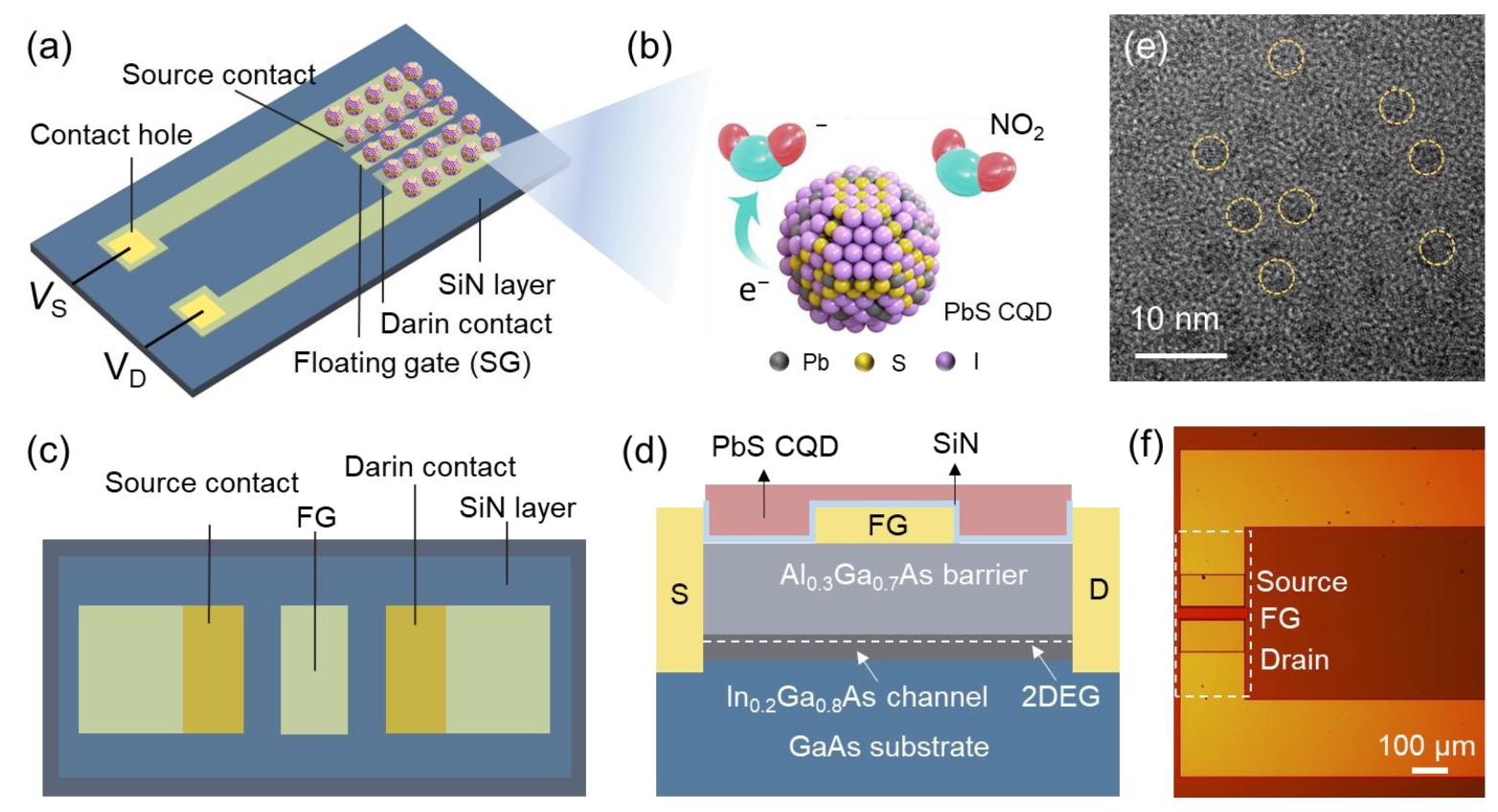
3.1. Operation Principle and Characterization of the Gas Sensor

A schematic of the PbS CQD-sensitized HEMT gas sensor is shown in Figure 1a. The device shares a basic structure and preparation process with the GaAs HEMT, as reported before [39], which includes an AlGaAs/InGaAs/GaAs epitaxial layer, source and drain electrodes, and a floating gate. Unlike conventional FET-type gas sensors, a SiN passivation layer was deposited on top of the sensor chip, and contact holes were fabricated on the source/drain electrode pad. The PbS CQDs, which act as the gas sensing material, were then deposited on top of the SiN passivation layer. When the PbS quantum dots are exposed to the target gas, gas molecules undergo charge transfer with the PbS quantum dots, affecting the surface charge of the interface (Figure 1b). This results in a change in the electronic characteristics of the quantum dot film, including resistance and capacitance.
Since the surface of the HEMT is encapsulated by a SiN passivation layer (Figure 1c,d), and the PbS CQD film is insulated from the source electrode, drain electrode, and floating gate, the resistance change will not affect the signal of the transistor. Therefore, the sensor operates based on the capacitance coupling effect, which will be further discussed below. As shown in Figure 1d, the PbS CQD sensing film is separated from the current-carrying two-dimensional electron gas (2DEG) [23], allowing the sensor to possess both higher sensitivity and a larger signal current.
The PbS CQDs were synthesized using a hot-injection method and were initially capped with oleic acid ligands to allow for good dispersibility in the octane solvent. However, these ligands will hinder electronic transport among the CQDs and prevent gas molecules from interacting with the CQDs. To overcome this limitation and promote gas adsorption, we employed a phase-transfer ligand exchange strategy to remove the original oleate ligand. The iodine ligand was introduced to passivate the surface of PbS CQDs, as it has been shown to improve the air stability of the PbS CQD-based gas sensor and optoelectronics [40]. Figure 1b illustrates the atomic-halide ligand passivated PbS CQD surface, where the halide anions can act as X-type ligands [41]. HRTEM characterization estimated the average diameter of the nanocrystals to be 3.5 nm (Figure 1e), indicating that the PbS CQDs have a large surface area capable of interacting with incoming gas. The GaAs HEMT in this study was grown using MBE on a GaAs substrate [39]. Figure 1f shows an optical microscope image of the HEMT sensor chip, which has a channel length of 40 μm and is passivated by a SiN insulation layer. To deposit the sensing film, a layer of PbS CQD is spin-coated onto the surface of the sensor chip.

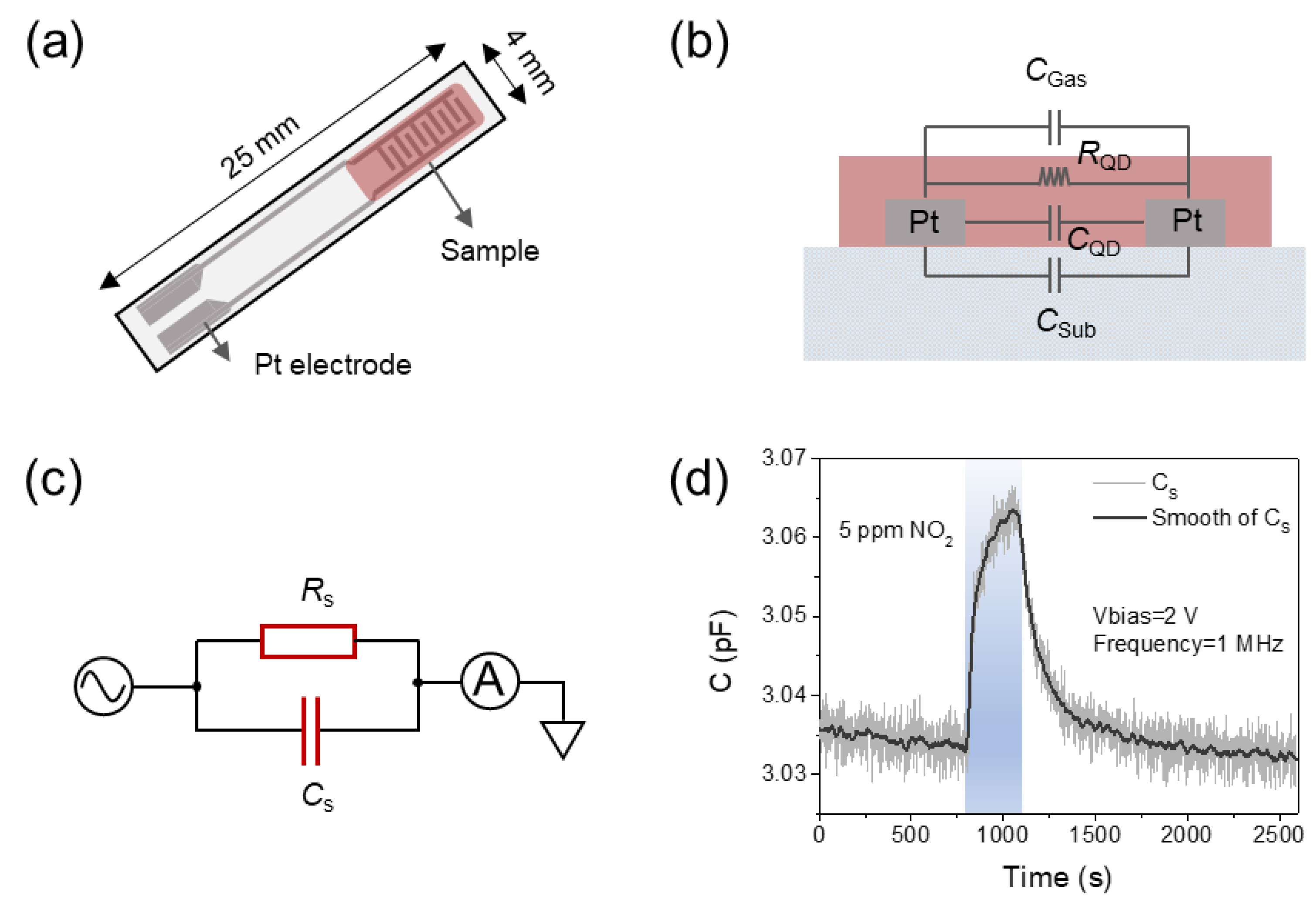
3.2. The Equivalent Circuit of the Gas Sensor

Based on the schematic diagram presented in Figure 1d, the quantum dot gas-sensitive film located between the floating gate and source/drain of the HEMT can be considered as two capacitors, CGS and CGD. The equivalent circuit diagram of the sensor is shown in Figure 2a, where UFG represents the gate potential originating from the capacitance coupling effect. Since CGS and CGD are connected in series, they form a voltage divider circuit. When the gate is floating, the gate potential UFG is not zero, and its magnitude is dependent on the source-drain voltage VD, CGS, and CGD.
To verify the equivalent circuit model, we investigated the ID-VD test curves of the sensor under two conditions: with a biased gate (blue line) and with a floating gate (red line), as presented in Figure 2b. The results clearly indicate that the ID-VD curve of the sensor with a biased gate does not align with the sensor with a floating gate. Moreover, at the same source-drain voltage, the drain current of the sensor with a floating gate is significantly higher than the sensor with a gate bias at 0 V. This observation can be explained by the induction of a gate potential when the gate is floating. Additionally, due to the coupling effect between the gate-source capacitance, CGS, and the gate-drain capacitance, CGD, the gate-drain voltage, VGS, under the floating gate condition satisfies Equation (1).
V GS = V D C GS C GS + C GD
For instance, when the source-drain voltage is 0.5 V, the measured drain current under the floating gate condition is comparable to that measured at a gate voltage of 0.3 V, as shown in Figure 2b. Figure 2c illustrates the relationship between the measured equivalent gate bias and the source-drain voltage under the floating gate condition. A linear fit of the equivalent gate voltage, VGS, and VD in the linear region yields a fitting slope of 0.574, with a fitting accuracy of 99.8%. This indicates that CGS/(CGS + CGD) = 0.574, which suggests that the source and drain terminals of the device are not symmetrical. Specifically, the gate-source capacitance, CGS, is slightly larger than the gate-drain capacitance, CGD.

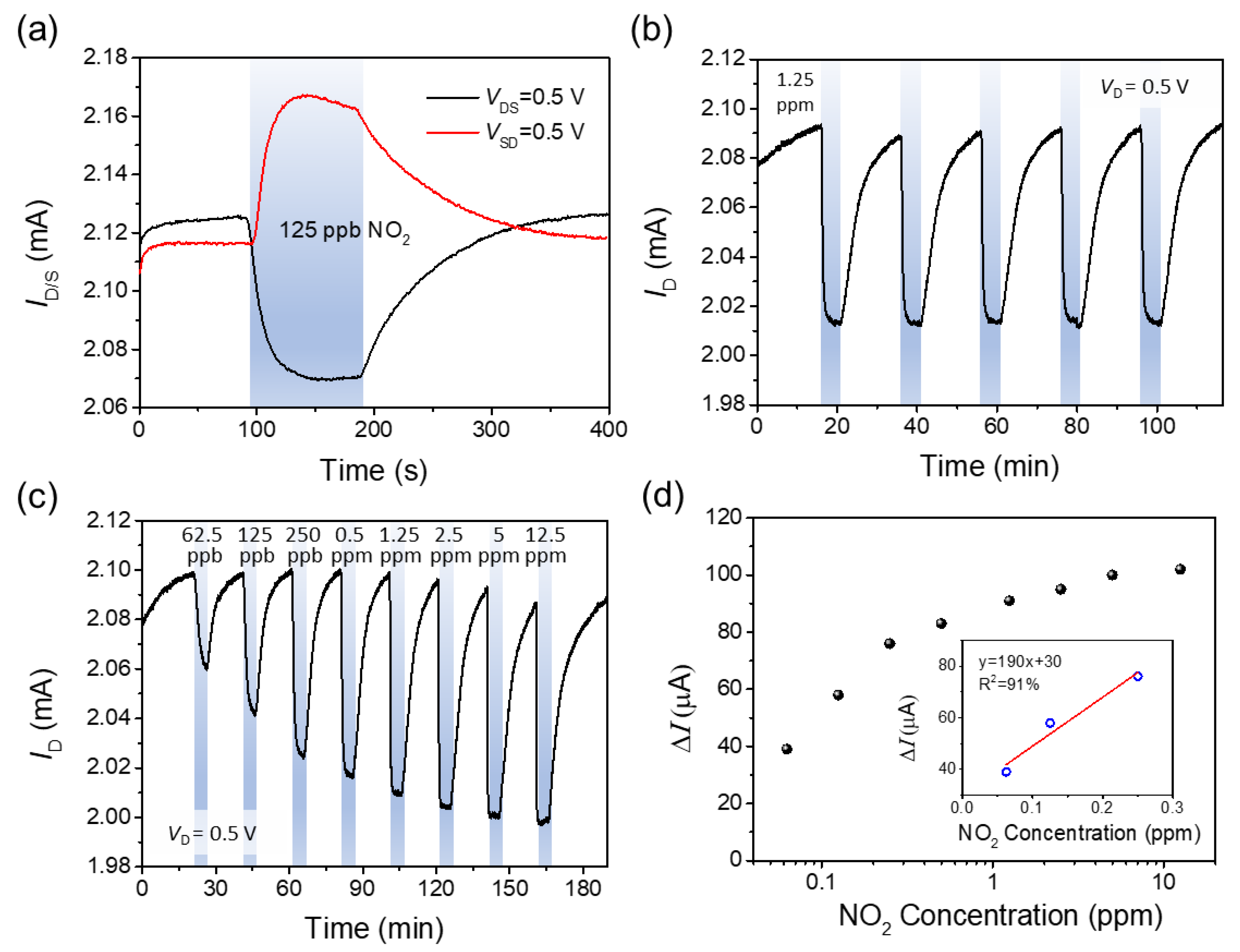
3.3. Sensing Properties of the Gas Sensor

The response characteristics of the PbS CQD-sensitized HEMT gas sensor to NO2 gas were tested at room temperature. Since the gate equivalent potential is influenced by the gate-source capacitance, gate-drain capacitance, and source-drain voltage, separate tests were conducted with the source electrode grounded and with the drain electrode grounded to investigate the gas-sensitive response characteristics of the sensor to NO2, as depicted in Figure 3a. When the source electrode was grounded and the drain electrode was biased at 0.5 V, the sensor’s drain current, ID, decreased rapidly when exposed to 125 ppb NO2. Conversely, when the drain was grounded and the source bias was 0.5 V, the sensor’s source current, ID, increased rapidly when exposed to 125 ppb NO2. Combined with the analysis of Equation (1), it can be inferred that when the sensor is exposed to the NO2 atmosphere, both the gate-source capacitance, CGS, and the gate-drain capacitance, CGD, will change, resulting in a change in the equivalent gate voltage, VGS, and a corresponding change in the drain current, ID:
I D = W μ n C 0 L V GS V th V DS 1 2 V DS 2
where W and L are the width and length of the gate, μ n is the electron mobility, C 0 is the gate capacitance, and V th is the threshold voltage of the HEMT. When the source and drain electrodes were exchanged for testing, the direction of change in the equivalent gate voltage, VGS, also changed, causing the response direction of the sensor to change.
As the change in the gate equivalent voltage was equal under the two test conditions, the change in source-drain current was very close, which was approximately 55 μA. The capacitance of the gate-drain capacitance in air was about 19.5 pF, and the value increased in NO2 (Figure S1). We also measured the leakage current of the PbS quantum dot film at a bias voltage of 0.5 V and found it to be around 0.3 nA (Figure S2). In the HEMT sensor, the quantum dots are isolated from the electrode by a SiN passivation layer, which significantly reduces the leakage current of the quantum dot film capacitance. Therefore, the leakage current of the PbS quantum dot film capacitance does not affect the performance of the device. By analyzing the slope of the transfer characteristic curve in the linear region (Figure S3), we determined the electron mobility of our sensor to be 4.86 × 103 cm2V−1s−1 (for calculation details, see the Supporting Information). This value indicates that the sensitivity and signal-to-noise ratio of our sensor will benefit from such high electron mobility.
Figure 3b presents the response curve of the gas sensor to 1.25 ppm NO2. The response of the sensor is defined as ΔI = I0Ig, where I0 is the drain current of the sensor in air, and Ig is the drain current of the sensor in NO2. The response and recovery times of the sensor are defined as the time required for a 90% change of the total change of the sensing response. The sensor shows fast response and recovery properties at room temperature; the response and recovery times are 52 s and 7 min, respectively. NO2 is a significant air pollutant, and the United States Environmental Protection Agency (EPA) has set stringent standards for its concentration, which is 100 ppb for a one-hour exposure [42]. We conducted a wide-range test of the sensor response to NO2 concentrations ranging from 62.5 ppb to 12.5 ppm (Figure 3c). The sensor’s drain current decreased with the increasing NO2 concentration. Figure 3d shows the relationship between the response ΔI and NO2 concentration, indicating that the sensor has a high sensitivity to low NO2 concentrations. By further performing linear fitting of the response values in the low concentration range, a slope of 190 was obtained. According to the formula for calculating the theoretical detection limit (LOD) [16], the LOD of the sensor was calculated to be 0.36 ppb, which suggests its potential for air pollution monitoring.
Furthermore, we conducted selectivity tests for the gas sensor. The tests were performed on 1.25 ppm NH3, SO2, acetone, and H2 at room temperature. The results showed that the sensor exhibited a highly selective responsive behavior towards NO2 (Figure S4). We further investigated the sensing performance of the sensor in moist environments (Figure S5). The results showed that the sensor had a lower response under relative humidity of 30% compared to that in dry air. However, the response increased with higher humidity levels and the highest response was observed at a relative humidity of 90%.

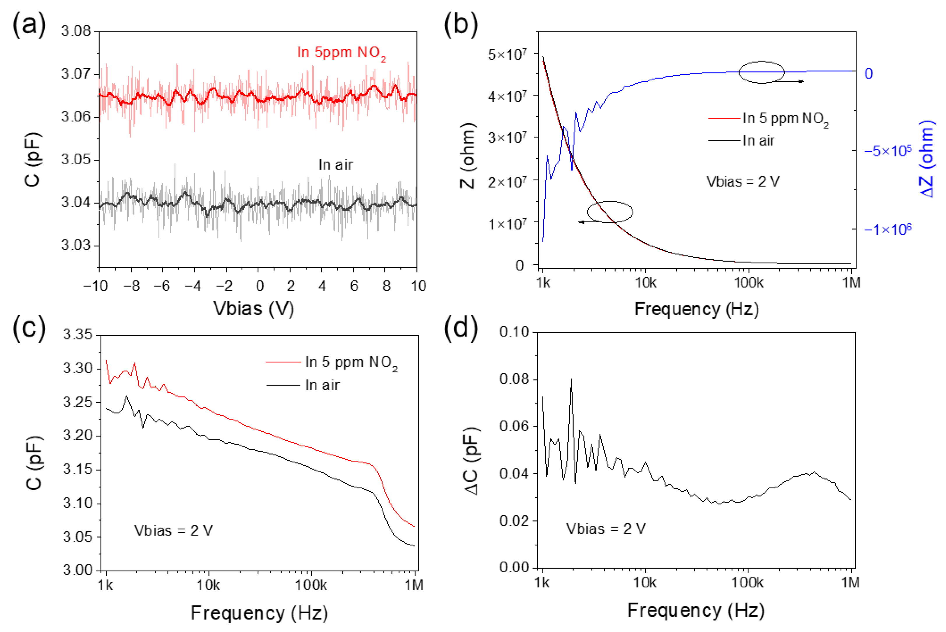
3.4. Investigation of the Capacitance Response of PbS CQDs

The capacitance response of PbS quantum dot thin films plays a crucial role in influencing the performance of field-effect transistor gas sensors, as the equivalent circuit in Figure 2a clearly demonstrates. The complex gate structure of GaAs HEMT sensors makes them unsuitable for examining the capacitance effects of PbS CQDs. Therefore, an interdigital electrode structure was fabricated to investigate the capacitance of the quantum dot film (Figure 4a). This device possesses a simple structure, and its capacitance response is solely dependent on the CQD film. The electric field between the electrodes is distributed in the surface space above and below the electrode plane, and changes in the surface space dielectric constant cause variations in the capacitance value of the interdigital capacitor. These changes can be further employed to analyze relevant physical or chemical quantities. By applying a wide-band AC voltage between the electrodes as an excitation signal, the impedance of the sensing film under wide-band excitation can be measured to obtain the electrical characteristics of the sensor.
The impedance contributions from different parts of the sensor are displayed in Figure 4b, where RQD is the resistance of the CQD sensing film, CGas is the parasitic capacitance generated by the atmosphere above the interdigital electrode, CQD is the capacitance of the quantum dot gas sensing film between the interdigital electrodes, and CSub is the parasitic capacitance generated by the Al2O3 ceramic substrate below the interdigital electrode. The sensor’s equivalent circuit diagram can be simplified as a parallel model of a resistor and capacitor, as depicted in Figure 4c, where RS corresponds to RQD and CS = CGas + CQD + CSub.
We examined the capacitive response of a PbS CQD film in the presence of NO2 gas. The basic principle of the test involved applying an AC bias voltage to the sensor electrodes and measuring the sensor’s impedance, Z, which comprises a real part (RS) and an imaginary part (X) such that Z = RS + jX = |Z|∠θ. The value of CS was calculated based on Z and θ. Figure 4d depicts the capacitance response curve of the PbS CQD film to 5 ppm NO2, with an excitation voltage frequency of 1 MHz and an amplitude of 2 V. The sensor’s capacitance value increases upon exposure to NO2 gas, and the sensor’s capacitance response is defined as ΔC = CgC0, where Cg is the capacitance value of the sensor in the NO2 atmosphere, and C0 is the capacitance value of the sensor in air. The capacitance response of the sensor to 5 ppm NO2 is 30 fF.
To investigate the impact of voltage excitation parameters on capacitance, we conducted further experiments to examine the effect of bias voltage on the capacitance testing of PbS quantum dots. The C-V curves of the PbS quantum dot gas sensor were obtained in both air and 5 ppm NO2 atmospheres, as shown in Figure 5a. The testing frequency was 1 MHz, and the testing bias voltage ranged from −10 V to 10 V. It was observed that the capacitance of the PbS quantum dot gas sensor was independent of the testing bias voltage, indicating that an Ohmic contact existed between the PbS quantum dots and Pt electrodes, and the impact of the potential barrier capacitance was negligible.
To investigate how the testing frequency affects the capacitance response of the PbS CQD, we conducted further tests to examine the impedance characteristics of the PbS CQD film in the frequency range of 1 kHz to 1 MHz. As shown in Figure 5b, we displayed the impedance-frequency curves of the PbS CQD film under air and NO2 atmospheres, respectively. The impedance of the PbS CQD film decreases as the frequency increases, and at low frequencies (lower than 10 kHz), the impedance exhibits significant background noise. This may be due to the small effective area of the cross-shaped electrode and the large sensor resistance, which cause the 1/f noise [27]. Furthermore, as depicted in Figure 5c, the sensor capacitance varied with the testing frequency. The capacitance of the sensor also decreases as the testing frequency increases and is more susceptible to background noise at low frequencies. The capacitance of the sensor shows a significant decreasing trend in the 400 kHz to 1 MHz frequency range. This trend could be attributed to the higher dielectric loss of the quantum dot material at this testing frequency range, reducing the effective dielectric constant between the electrodes and leading to decreased device capacitance.
Figure 5d shows the relationship between the capacitance response of the sensor and the testing frequency. The sensor has a higher capacitance response at low frequencies (lower than 10 kHz) but also exhibits larger background noise. In the frequency range above 10 kHz, the capacitance response of the sensor first increases and then decreases, with the highest capacitance response at the testing frequency of 400 kHz. Therefore, from the perspective of sensitivity and signal stability, selecting an input voltage of 400 kHz for testing can obtain a high sensitivity and high signal-to-noise ratio for the sensor signal.

3.5. The Capacitance Response Mechanism of PbS CQD

Based on the equivalent circuit model shown in Figure 5c, the capacitance of the PbS CQD film can be calculated as the sum of the capacitances of the quantum dot film and the parasitic capacitance, CS = CGas + CQD + CSub. During the testing process, the parasitic capacitance, CSub, of the ceramic substrate remains constant, so the capacitance response of the sensor is mainly determined by the gas atmosphere capacitance, CGas, and the quantum dot film capacitance, CQD. As gas molecules possess dipole moments, changes in the gas composition can alter the dielectric constant of the gas and, consequently, affect the CGas. This relationship is described by Equations (3) to (5) [43].
C = ε r S 4 π kd = ε r ε 0 S d = ε S d
ε = 4 π N γ 1 4 π 3 N γ
γ = γ mol + μ 2 3 k T
Here, μ represents the dipole moment of a single gas molecule, γ represents the polarization degree of a single gas molecule, and γ mol is the intrinsic polarization degree of a gas molecule. As the gas sensor in this study is based on a planar interdigitated electrode structure, the electric field lines mainly distribute in the quantum dot film and the ceramic substrate. Therefore, the capacitance change, CGas, caused by different gas molecules can be neglected compared to the quantum dot film capacitance, CQD, as the former is very small. Due to the constant parasitic capacitance of the ceramic substrate, CSub, the capacitance response, ΔCS, of the PbS quantum dot gas sensor is equal to the capacitance change, ΔCQD, of the quantum dots.
After gas molecules are adsorbed onto the surface of quantum dots, a polarized layer is formed, which increases the capacitance of the quantum dot film. The degree of polarization of the polarized layer is proportional to P P 0 e E b E i / k T , where P P 0 represents the ratio of the gas pressure to the reference pressure, Ei and Eb represent the interaction energy between the gas molecules and the binding energy between the gas molecules and sensing materials, respectively [43]. Due to the strong binding energy between NO2 and the PbS quantum dots, the film demonstrates a highly responsive capacitance to NO2 gas.
The capacitance of the quantum dots is also influenced by the surface states resulting from gas-solid interactions. The interaction between the gas molecules and quantum dots changes the density of states of the quantum dots, which in turn alters their quantum capacitance, denoted as CQ [43]. Quantum capacitance refers to the ability of a material’s quantum states to accommodate electrons. When a system is charged, it accumulates charge. At absolute zero, the quantum capacitance can be simplified as [30]:
C Q = q 2 g E F
where the density of states of the quantum dots is represented by g E F . Therefore, it can be observed that when thermally excited charge carriers are disregarded, the material’s quantum capacitance is proportional to the density of states.
All materials, including conductors, possess quantum capacitance. The effective capacitance of a material, Ceff, is the series capacitance formed by the quantum capacitance, CQ, and the traditional geometric capacitance, Cgeo [44]. In conventional material systems, such as bulk semiconductors or metals, their density of states (DOS) is sufficiently high, and the accumulation of limited charges is insufficient to cause a significant shift in the Fermi level. These materials have a strong ability to accommodate electrons, and their quantum capacitance, CQ, is infinite (Figure 6a). According to the capacitance series calculation formula, 1 C eff = 1 C Q + 1 C geo , the effective capacitance, Ceff, is independent of their quantum capacitance. Therefore, the influence of quantum capacitance is only significant in materials with low state densities. In low-dimensional semiconductor systems, such as quantum dots, the energy levels of their electrons become discrete quantized levels due to the quantum confinement effect. The electron state density is low, and the Fermi level needs to shift significantly to accumulate a certain amount of charge carriers in the material. Therefore, the quantum capacitance, CQ, of these materials is small (Figure 6b). When its value is comparable to the geometric capacitance, Cgeo, of the material, it significantly affects the total capacitance of the material.
Overall, the capacitance response of the PbS quantum dot gas sensing film can be expressed as Δ C C ϵ Δ ϵ + C Q Δ Q , where the former term is related to the dielectric effect of the adsorbed gas molecules and the latter is related to the charge transfer caused by the quantum capacitance, CQ, of the quantum dots. NO2 gas molecules have strong binding energy with PbS quantum dots, and after being adsorbed onto the surface of the quantum dots, they interact with them, resulting in charge transfer and the formation of a polarization layer, which increases the capacitance of the gas sensing film. Our prior research has shown that the adsorption of NO2 gas molecules onto the surface of PbS quantum dots results in an increased density of states [16]. This increase causes a charge-transfer-driven p-type doping effect. According to Equation (6), it can be inferred that the quantum capacitance of PbS quantum dots increases, and as a result, the capacitance of the quantum dot film is further increased due to the effect of quantum capacitance.
Our findings suggest that the interdigital electrode structure on the alumina substrate-based capacitive gas sensor possesses a simple structure and is cost-effective, which makes it a suitable platform for researching the capacitance characteristics and mechanisms of nanomaterials. However, specialized equipment is necessary for testing. On the other hand, the proposed gate-sensitive HEMT gas sensor is compatible with microelectronic manufacturing technology, has a small size, has high integration, and can amplify sensor signals through the FET, enabling integration with on-chip readout circuits (ROIC). Therefore, the proposed gate-sensitive HEMT gas sensor has enormous potential for practical applications.

4. Conclusions

We have successfully developed a novel quantum dots-sensitized HEMT gas sensor with exceptional sensitivity to NO2 at room temperature. By utilizing the capacitance coupling effect of the quantum dots sensing film based on a floating gate, our FET-type gas sensor effectively separates the gate sensing film from the 2DEG conduction channel, resulting in a theoretical LOD of 0.36 ppb. Moreover, the sensor provides a high signal-to-noise ratio readout current at milliampere, allowing for easy integration with readout circuits. The unique surface effects and quantum capacitance effects of the quantum dots make them a promising candidate for the development of high-performance on-chip gas sensors. Overall, these results suggest that our novel gas sensor has the potential to significantly advance the field of gas sensing technology, opening new possibilities for a wide range of applications.

Supplementary Materials

The following supporting information can be downloaded at: https://www.mdpi.com/article/10.3390/chemosensors11040252/s1, Figure S1: The gate-drain capacitance, CGD, in response to 5 ppm NO2; Figure S2: Leakage current test of the PbS CQD film; Figure S3: ID-VG curve of the GaAs HEMT; Figure S4: Response of the sensor to different target gases at room temperature; Figure S5: The sensor’s response to 1.25 ppm NO2 was tested under relative humidity ranging from 0 to 90%.

Author Contributions

Conceptualization, H.L. (Huayao Li), Y.Z. (Yang Zhang) and H.L. (Huan Liu); methodology, H.L. (Huan Liu); software, Z.H., B.Y. and Y.Z. (Yunong Zhao); formal analysis, Z.H. and L.Z.; investigation, Z.H., L.Z., L.L., B.Y., Y.Z. (Yunong Zhao) and P.W.; resources, Y.Z. (Yang Zhang) and H.L. (Huan Liu); data curation, Z.H., L.Z., L.L. and P.W.; writing—original draft preparation, Z.H.; writing—review and editing, Y.Z. (Yang Zhang) and H.L. (Huan Liu); supervision, H.L. (Huayao Li), Y.Z. (Yang Zhang) and H.L. (Huan Liu); funding acquisition, H.L. (Huayao Li), Y.Z. (Yang Zhang) and H.L. (Huan Liu). All authors have read and agreed to the published version of the manuscript.

Funding

This work was supported by the National Natural Science Foundation of China (Grant No. 61922032, 62271222, and 61904062). We are thankful for the support from the Youth Innovation Promotion Association of the Chinese Academy of Sciences (Grant No. 2015094). We are thankful for the support from the Hubei Provincial Natural Science Foundation of China (Grant No. 2022CFA035). We are thankful for the support from the Zhejiang Provincial Natural Science Foundation of China (Grant No. LY23F040006). We thank the Program for HUST Academic Frontier Youth Team (2018QYTD06) and the Innovation Fund of WNLO.

Institutional Review Board Statement

Not applicable.

Informed Consent Statement

Not applicable.

Data Availability Statement

The data presented in this study are available on request from the corresponding author.

Acknowledgments

We acknowledge the facility and technical assistance from the Analytical and Testing Center of HUST.

Conflicts of Interest

The authors declare no conflict of interest.

References

  1. Potyrailo, R.A. Multivariable Sensors for Ubiquitous Monitoring of Gases in the Era of Internet of Things and Industrial Internet. Chem. Rev. 2016, 116, 11877–11923. [Google Scholar] [CrossRef] [PubMed]
  2. Wang, G.; Li, Y.; Cai, Z.; Dou, X. A Colorimetric Artificial Olfactory System for Airborne Improvised Explosive Identification. Adv. Mater. 2020, 32, 1907043. [Google Scholar] [CrossRef] [PubMed]
  3. Machado, R.F.; Laskowski, D.; Deffenderfer, O.; Burch, T.; Zheng, S.; Mazzone, P.J.; Mekhail, T.; Jennings, C.; Stoller, J.K.; Pyle, J.; et al. Detection of Lung Cancer by Sensor Array Analyses of Exhaled Breath. Am. J. Respir. Crit. Care Med. 2005, 171, 1286–1291. [Google Scholar] [CrossRef] [PubMed]
  4. Guo, L.; Wang, T.; Wu, Z.; Wang, J.; Wang, M.; Cui, Z.; Ji, S.; Cai, J.; Xu, C.; Chen, X. Portable Food-Freshness Prediction Platform Based on Colorimetric Barcode Combinatorics and Deep Convolutional Neural Networks. Adv. Mater. 2020, 32, 2004805. [Google Scholar] [CrossRef]
  5. Kalantar-Zadeh, K.; Berean, K.J.; Ha, N.; Chrimes, A.F.; Xu, K.; Grando, D.; Ou, J.Z.; Pillai, N.; Campbell, J.L.; Brkljača, R.; et al. A Human Pilot Trial of Ingestible Electronic Capsules Capable of Sensing Different Gases in the Gut. Nat. Electron. 2018, 1, 79–87. [Google Scholar] [CrossRef]
  6. Kim, H.; Lee, J. Highly sensitive and selective gas sensors using p-type oxide semiconductors: Overview. Sens. Actuators B Chem. 2014, 192, 607–627. [Google Scholar] [CrossRef]
  7. Potyrailo, R.A.; Go, S.; Sexton, D.; Li, X.; Alkadi, N.; Kolmakov, A.; Amm, B.; St-Pierre, R.; Scherer, B.; Nayeri, M.; et al. Extraordinary performance of semiconducting metal oxide gas sensors using dielectric excitation. Nat. Electron. 2020, 3, 280–289. [Google Scholar] [CrossRef]
  8. Feng, Q.; Zeng, Y.; Xu, P.; Lin, S.; Feng, C.; Li, X.; Wang, J. Tuning the electrical conductivity of amorphous carbon/reduced graphene oxide wrapped-Co3O4 ternary nanofibers for highly sensitive chemical sensors. J. Mater. Chem. A 2019, 7, 27522–27534. [Google Scholar] [CrossRef]
  9. Mirzaei, A.; Kordrostami, Z.; Shahbaz, M.; Kim, J.; Kim, H.W.; Kim, S.S. Resistive-Based Gas Sensors Using Quantum Dots: A Review. Sensors 2022, 22, 4369. [Google Scholar] [CrossRef]
  10. Hong, S.; Huang, Q.; Wu, T. The Room Temperature Highly Sensitive Ammonia Gas Sensor Based on Polyaniline and Nitrogen-Doped Graphene Quantum Dot-Coated Hollow Indium Oxide Nanofiber Composite. Polymers 2021, 13, 3676. [Google Scholar] [CrossRef]
  11. Carbone, M. CQDs@NiO: An Efficient Tool for CH4 Sensing. Appl. Sci. 2020, 10, 6251. [Google Scholar] [CrossRef]
  12. Galstyan, V. “Quantum dots: Perspectives in next-generation chemical gas sensors”—A review. Anal. Chim. Acta 2021, 1152, 238192. [Google Scholar] [CrossRef] [PubMed]
  13. Mitri, F.; De Iacovo, A.; De Luca, M.; Pecora, A.; Colace, L. Lead sulphide colloidal quantum dots for room temperature NO2 gas sensors. Sci. Rep. 2020, 10, 12556. [Google Scholar] [CrossRef]
  14. Liu, J.; Hu, Z.; Zhang, Y.; Li, H.; Gao, N.; Tian, Z.; Zhou, L.; Zhang, B.; Tang, J.; Zhang, J.; et al. MoS2 Nanosheets Sensitized with Quantum Dots for Room-Temperature Gas Sensors. Nano-Micro Lett. 2020, 12, 59. [Google Scholar] [CrossRef]
  15. Chen, R.; Wang, J.; Xia, Y.; Xiang, L. Near Infrared Light Enhanced Room-temperature NO2 Gas Sensing by Hierarchical ZnO Nanorods Functionalized with PbS Quantum Dots. Sens. Actuators B Chem. 2018, 255, 2538–2545. [Google Scholar] [CrossRef]
  16. Liu, H.; Li, M.; Voznyy, O.; Hu, L.; Fu, Q.; Zhou, D.; Xia, Z.; Sargent, E.H.; Tang, J. Physically Flexible, Rapid-Response Gas Sensor Based on Colloidal Quantum Dot Solids. Adv. Mater. 2014, 26, 2718–2724. [Google Scholar] [CrossRef]
  17. Martin-Pozas, T.; Sanchez-Moral, S.; Cuezva, S.; Jurado, V.; Saiz-Jimenez, C.; Perez-Lopez, R.; Carrey, R.; Otero, N.; Giesemann, A.; Well, R.; et al. Biologically Mediated Release of Endogenous N2O and NO2 Gases in a Hydrothermal, Hypoxic Subterranean Environment. Sci. Total Environ. 2020, 747, 141218. [Google Scholar] [CrossRef]
  18. Russ, T.; Hu, Z.; Junker, B.; Liu, H.; Weimar, U.; Barsan, N. Operando Investigation of the Aging Mechanism of Lead Sulfide Colloidal Quantum Dots in an Oxidizing Background. J. Phys. Chem. C 2021, 125, 19847–19857. [Google Scholar] [CrossRef]
  19. Liu, M.; Yazdani, N.; Yarema, M.; Jansen, M.; Wood, V.; Sargent, E.H. Colloidal Quantum Dot Electronics. Nat. Electron. 2021, 4, 548–558. [Google Scholar] [CrossRef]
  20. Radhakrishnan, K.; Ranjan, A.; Lingaparthi, R.; Dharmarasu, N. Enhanced NO2 Gas Sensing Performance of Multigate Pt/AlGaN/GaN High Electron Mobility Transistors. J. Electrochem. Soc. 2021, 168, 047502. [Google Scholar] [CrossRef]
  21. Fahad, H.M.; Gupta, N.; Han, R.; Desai, S.B.; Javey, A. Highly Sensitive Bulk Silicon Chemical Sensors with Sub-5 nm Thin Charge Inversion Layers. ACS Nano 2018, 12, 2948–2954. [Google Scholar] [CrossRef] [PubMed]
  22. Jung, S.; Baik, K.H.; Ren, F.; Pearton, S.J.; Jang, S. Detection of Ammonia at Low Concentrations (0.1–2 ppm) with ZnO Nanorod-Functionalized AlGaN/GaN High Electron Mobility Transistors. J. Vac. Sci. Technol. B Nanotechnol. Microelectron. 2017, 35, 42201. [Google Scholar] [CrossRef]
  23. Bishop, C.; Halfaya, Y.; Soltani, A.; Sundaram, S.; Li, X.; Streque, J.; El Gmili, Y.; Voss, P.L.; Salvestrini, J.P.; Ougazzaden, A. Experimental Study and Device Design of NO, NO2, and NH3 Gas Detection for a Wide Dynamic and Large Temperature Range Using Pt/AlGaN/GaN HEMT. IEEE Sens. J. 2016, 16, 6828–6838. [Google Scholar] [CrossRef]
  24. Ayadi, Y.; Rahhal, L.; Vilquin, B.; Chevalier, C.; Ambriz Vargas, F.; Ecoffey, S.; Ruediger, A.; Sarkissian, A.; Monfray, S.; Cloarec, J.; et al. Novel Concept of Gas Sensitivity Characterization of Materials Suited for Implementation in FET-Based Gas Sensors. Nanoscale Res. Lett. 2016, 11, 481. [Google Scholar] [CrossRef] [PubMed]
  25. Hong, S.; Wu, M.; Hong, Y.; Jeong, Y.; Jung, G.; Shin, W.; Park, J.; Kim, D.; Jang, D.; Lee, J. FET-type gas sensors: A review. Sens. Actuators B Chem. 2021, 330, 129240. [Google Scholar] [CrossRef]
  26. Zhang, P.; Xiao, Y.; Zhang, J.; Liu, B.; Ma, X.; Wang, Y. Highly Sensitive Gas Sensing Platforms based on Field effect Transistor-A Review. Anal. Chim. Acta 2021, 1172, 338575. [Google Scholar] [CrossRef]
  27. Mukherjee, A.; Rosenwaks, Y. Recent Advances in Silicon FET Devices for Gas and Volatile Organic Compound Sensing. Chemosensors 2021, 9, 260. [Google Scholar] [CrossRef]
  28. Lundstrom, I.; Sundgren, H.; Winquist, F.; Eriksson, M.; Krantzrulcker, C.; Lloydspetz, A. Twenty-five Years of Field Effect Gas Sensor Research in Linköping. Sens. Actuators B Chem. 2007, 121, 247–262. [Google Scholar] [CrossRef]
  29. Wilbertz, C.; Frerichs, H.P.; Freund, I.; Lehmann, M. Suspended-Gate- and Lundstrom-FET Integrated on a CMOS-chip. Sens. Actuators A Phys. 2005, 123–124, 2–6. [Google Scholar] [CrossRef]
  30. Gergintschew, Z.; Kornetzky, P.; Schipanski, D. The Capacitively Controlled Field Effect Transistor (CCFET) as a New Low Power Gas Sensor. Sens. Actuators B Chem. 1996, 36, 285–289. [Google Scholar] [CrossRef]
  31. Burgmair, M.; Frerichs, H.P.; Zimmer, M.; Lehmann, M.; Eisele, I. Field Effect Transducers for Work Function Gas Measurements: Device Improvements and Comparison of Performance. Sens. Actuators B Chem. 2003, 95, 183–188. [Google Scholar] [CrossRef]
  32. Hong, S.; Shin, J.; Hong, Y.; Wu, M.; Jang, D.; Jeong, Y.; Jung, G.; Bae, J.; Jang, H.W.; Lee, J. Observation of Physisorption in a High-performance FET-type Oxygen Gas Sensor Operating at Room Temperature. Nanoscale 2018, 10, 18019–18027. [Google Scholar] [CrossRef] [PubMed]
  33. Shin, W.; Hong, S.; Jeong, Y.; Jung, G.; Park, J.; Kim, D.; Lee, C.; Park, B.G.; Lee, J.H. Effect of Charge Storage Engineering on the NO2 Gas Sensing Properties of a WO3 FET-type Gas Sensor with a Horizontal Floating-gate. Nanoscale 2021, 13, 9009–9017. [Google Scholar] [CrossRef] [PubMed]
  34. Jung, G.; Shin, W.; Hong, S.; Jeong, Y.; Park, J.; Kim, D.; Bae, J.; Park, B.; Lee, J. Comparison of The Characteristics of Semiconductor Gas Sensors with Different Transducers Fabricated on the Same Substrate. Sens. Actuators B Chem. 2021, 335, 129661. [Google Scholar] [CrossRef]
  35. Hong, Y.; Wu, M.; Bae, J.; Hong, S.; Jeong, Y.; Jang, D.; Kim, J.S.; Hwang, C.S.; Park, B.; Lee, J. A New Sensing Mechanism of Si FET-based Gas Sensor Using Pre-bias. Sens. Actuators B Chem. 2020, 302, 127147. [Google Scholar] [CrossRef]
  36. Shin, W.; Jung, G.; Hong, S.; Jeong, Y.; Park, J.; Kim, D.; Jang, D.; Kwon, D.; Bae, J.H.; Park, B.G.; et al. Proposition of Deposition and Bias Conditions for Optimal Signal-to-noise-ratio in Resistor- and FET-type Gas Sensors. Nanoscale 2020, 12, 19768–19775. [Google Scholar] [CrossRef]
  37. Kim, C.H.; Cho, I.T.; Shin, J.M.; Choi, K.B.; Lee, J.K.; Lee, J.H. A New Gas Sensor Based on MOSFET Having a Horizontal Floating-Gate. IEEE Electron Device Lett. 2014, 35, 265–267. [Google Scholar] [CrossRef]
  38. Liu, M.; Voznyy, O.; Sabatini, R.; García De Arquer, F.P.; Munir, R.; Balawi, A.H.; Lan, X.; Fan, F.; Walters, G.; Kirmani, A.R.; et al. Hybrid Organic–inorganic Inks Flatten the Energy Landscape in Colloidal Quantum Dot Solids. Nat. Mater. 2017, 16, 258–263. [Google Scholar] [CrossRef]
  39. Xu, M.; Guan, M.; Cui, N.; Zhao, C.; Zhang, Y.; Zeng, Y.; Li, S. The GaAs/AlGaAs-Based Extended Gate HEMT Cardiac Troponin-I Biosensor: Design, Mechanism and Clinical Detection. IEEE Sens. J. 2021, 21, 18410–18416. [Google Scholar] [CrossRef]
  40. Ning, Z.; Voznyy, O.; Pan, J.; Hoogland, S.; Adinolfi, V.; Xu, J.; Li, M.; Kirmani, A.R.; Sun, J.; Minor, J.; et al. Air-stable n-type Colloidal Quantum Dot Solids. Nat. Mater. 2014, 13, 822–828. [Google Scholar] [CrossRef]
  41. Owen, J. The Coordination Chemistry of Nanocrystal Surfaces. Science 2015, 347, 614–615. [Google Scholar] [CrossRef] [PubMed]
  42. Childers, A. EPA Announces First One-Hour Standard for Nitrogen Dioxide at 0.10 Part per Million. Environ. Rep. 2010, 41, 197–198. [Google Scholar]
  43. Snow, E.S.; Perkins, F.K.; Houser, E.J.; Badescu, S.C.; Reinecke, T.L. Chemical Detection with a Single-walled Carbon Nanotube Capacitor. Science 2005, 307, 1942–1945. [Google Scholar] [CrossRef] [PubMed]
  44. Hanlumyuang, Y.; Sharma, P. Quantum Capacitance: A Perspective from Physics to Nanoelectronics. Jom 2014, 66, 660–663. [Google Scholar] [CrossRef]
Figure 1. Illustration of the proposed quantum dot gate-sensitive HEMT gas sensor. (a) Three-dimensional diagram of the gas sensor showing the AlGaAs/InGaAs/GaAs epitaxial layer, the source and drain electrodes, the floating gate, the SiN passivation layer, and the PbS quantum dot film; (b) Schematic of the sensing mechanism of PbS quantum dots to NO2 gas; (c) Schematic top view of the sensor chip; (d) Schematic cross-section of the sensor chip; (e) HRTEM image of PbS CQDs, the CQDs were circled by the yellow dotted line; (f) Optical microscope image of the sensor chip.
Chemosensors 11 00252 g001
Figure 2. Equivalent circuit of the gas sensor. (a) The equivalent circuit diagram of the sensor; (b) The ID-VD curve of the field-effect transistor sensor, and (c) the relationship between the equivalent gate voltage, VGS, and the drain voltage when the gate is floating.
Chemosensors 11 00252 g002
Figure 3. Sensing properties of the gas sensor. (a) Response curves of the sensor to 125 ppb NO2; Response curves of the gate-sensitive HEMT gas sensor to (b) 1.25 ppm and (c) 62.5 ppb~12.5 ppm NO2; (d) Relationship between the response of the sensor and the concentration of NO2.
Chemosensors 11 00252 g003
Figure 4. PbS quantum dot planar interdigitated capacitor gas sensor. (a) Schematic diagram of the structure; (b) Cross-sectional schematic diagram and impedance contributions; (c) Equivalent circuit model simplifying to a resistor-capacitor parallel model; (d) Capacitance response of PbS quantum dot gas sensor to 5 ppm NO2.
Chemosensors 11 00252 g004
Figure 5. Electrical properties of PbS CQDs gas sensor. (a) C-V characteristics of PbS quantum dot gas sensor in air and 5 ppm NO2 atmospheres at 1 MHz and bias voltage range of −10 V to 10 V; (b) Impedance-frequency curves of the PbS CQD film under air and NO2 atmospheres at frequency range of 1 kHz to 1 MHz; (c) Capacitance-frequency curves of the PbS CQD film under air and NO2 atmospheres at frequency range of 1 kHz to 1 MHz; (d) Capacitance response of PbS CQD gas sensor at different test frequencies (1 kHz to 1 MHz).
Chemosensors 11 00252 g005
Figure 6. Relationship between quantum capacitance and density of states. (a) For bulk materials, the variation in electron concentration has a limited impact on the position of the Fermi level, and the quantum capacitance is large; (b) For quantum dots, electron gain and loss can cause a significant change in the Fermi level position, and the quantum capacitance is small.
Chemosensors 11 00252 g006
Disclaimer/Publisher’s Note: The statements, opinions and data contained in all publications are solely those of the individual author(s) and contributor(s) and not of MDPI and/or the editor(s). MDPI and/or the editor(s) disclaim responsibility for any injury to people or property resulting from any ideas, methods, instructions or products referred to in the content.

