
Metal Oxide Semiconductor Nanostructure Gas Sensors with Different Morphologies

 ,
,  ,
,
Abstract
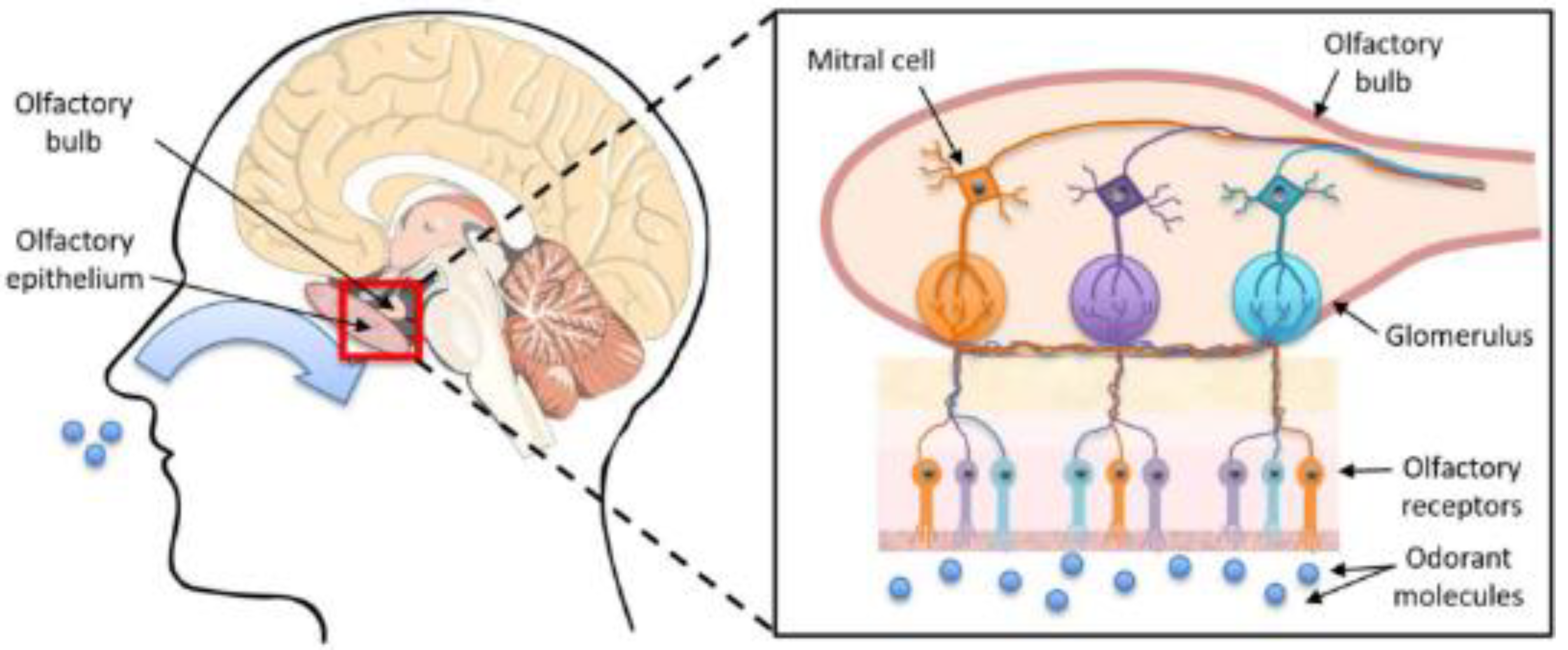
:1. Introduction
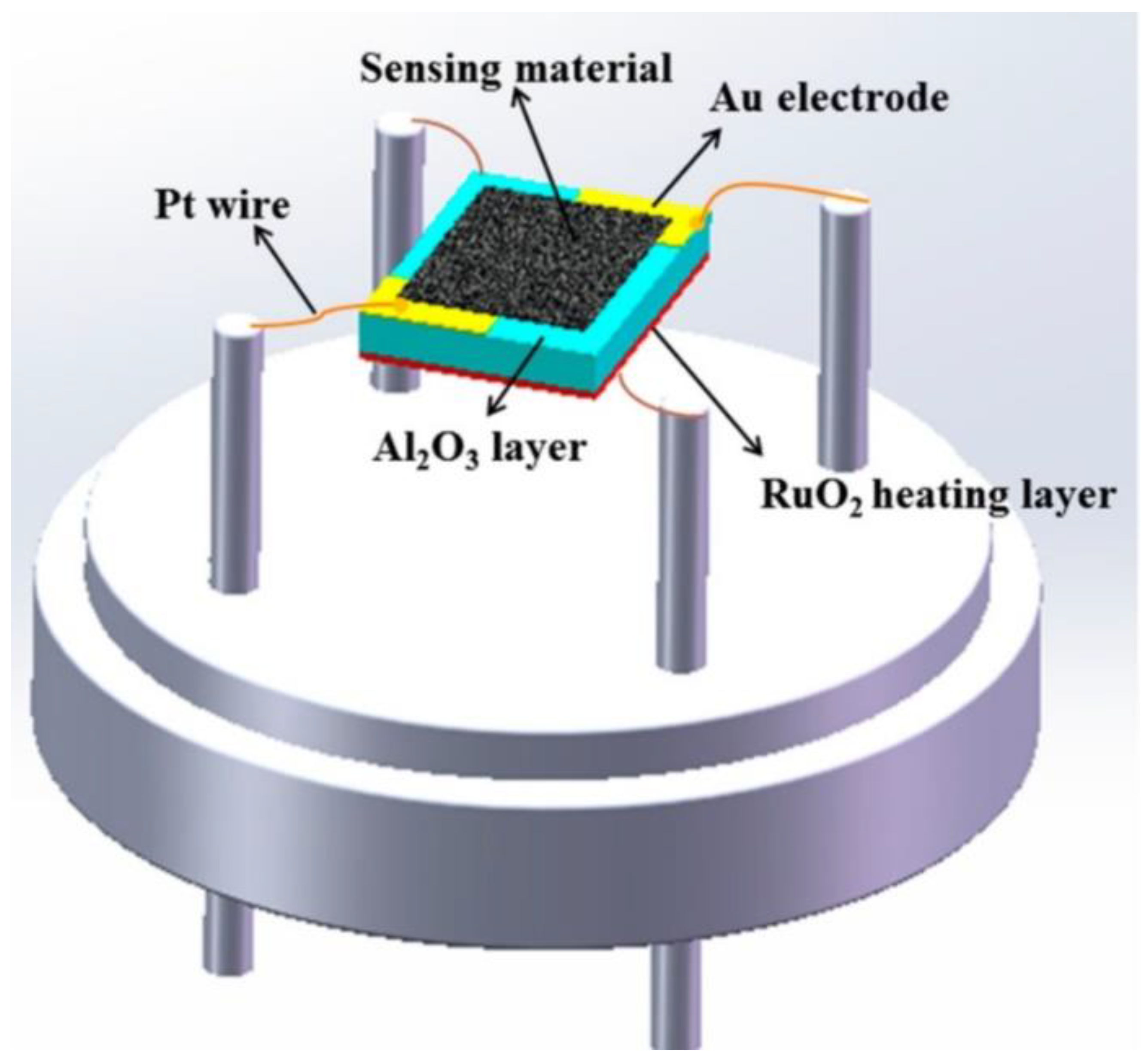
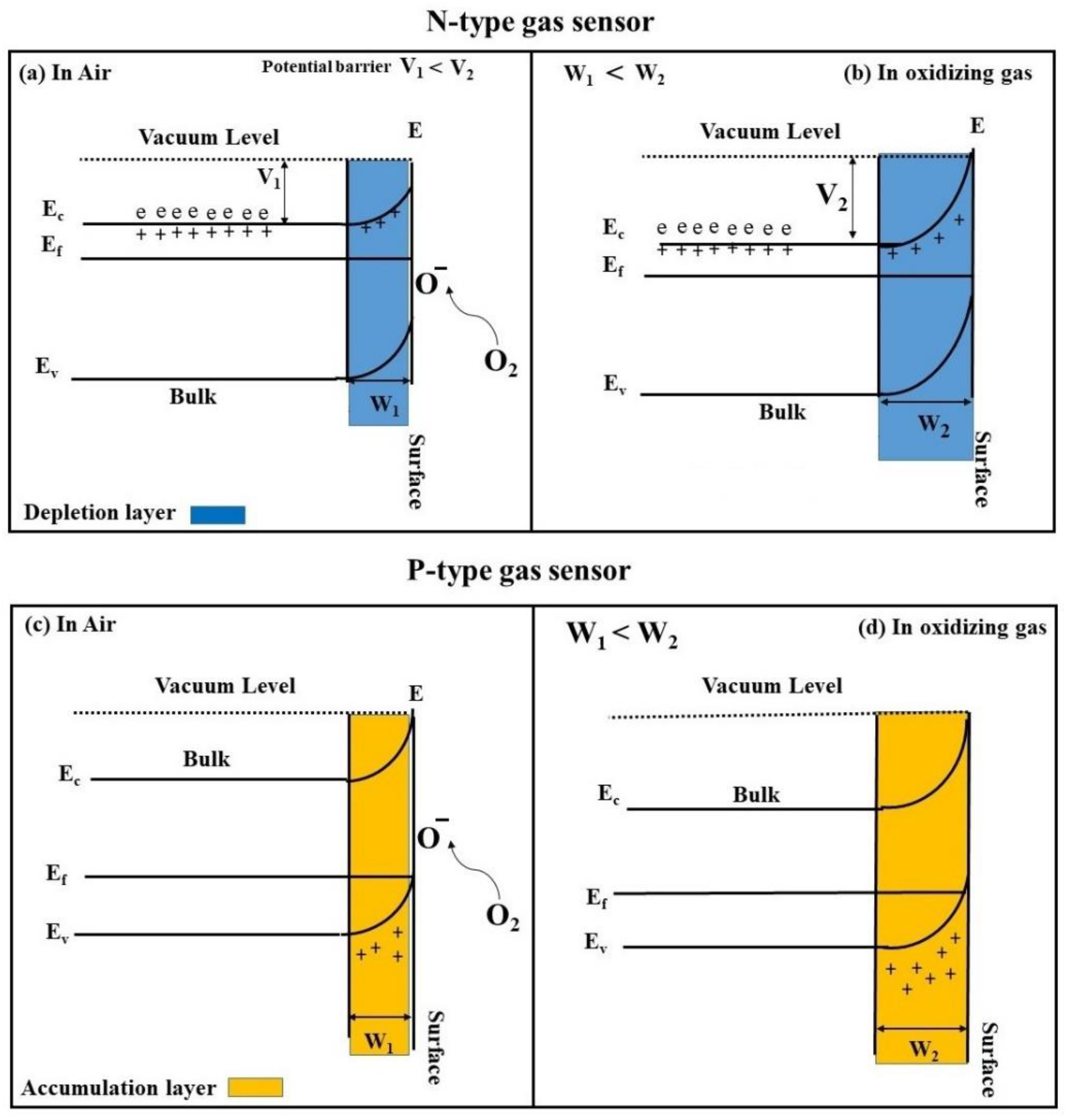
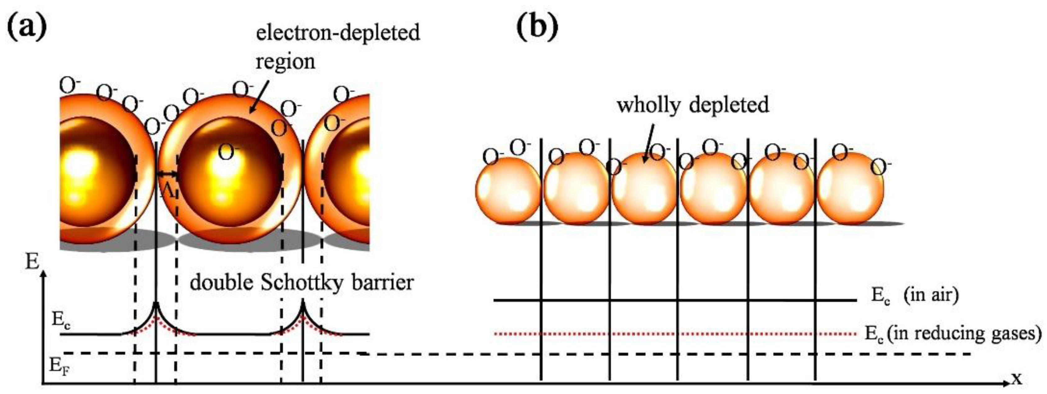
2. MOS-Based Gas Sensors with Different Morphologies
2.1. Quantum-Dot-Based Gas Sensors Using MOSs
2.2. Nanowire-Based Nanomaterial Gas Sensors
2.3. Nanofiber-Based MOS Gas Sensors
2.4. Nanotube-Based MOS Gas Sensors
2.5. Nanorod-Based MOS Gas Sensors
2.6. Nanosheet-Based MOS Gas Sensors
2.7. Three-Dimensional MOS Gas Sensors
2.8. Noble-Metal-Decorated MOS Gas Sensors
2.9. Hybrid MOS Gas Sensors
2.10. Comparison of Performance of Gas Sensors with Different Morphologies
3. Conclusions and Outlooks
Author Contributions
Funding
Institutional Review Board Statement
Informed Consent Statement
Acknowledgments
Conflicts of Interest
References
- Kampa, M.; Castanas, E. Human health effects of air pollution. Environ. Pollut. 2008, 151, 362–367. [Google Scholar] [CrossRef] [PubMed]
- Paralovo, S.L.; Barbosa, C.G.G.; Carneiro, I.P.S.; Kurzlop, P.; Borillo, G.C.; Schiochet, M.F.C.; Godoi, A.F.L.; Yamamoto, C.I.; de Souza, R.A.F.; Andreoli, R.V. Observations of particulate matter, NO2, SO2, O3, H2S and selected VOCs at a semi-urban environment in the Amazon region. Sci. Total Environ. 2019, 650, 996–1006. [Google Scholar] [CrossRef] [PubMed]
- Jung, S.J.; Mehta, J.S.; Tong, L. Effects of environment pollution on the ocular surface. Ocul. Surf. 2018, 16, 198–205. [Google Scholar] [CrossRef]
- Elizabeth, F.Y.; Kenneth, Z.; Naus, A.; Forbes, C.; Wu, X.; Dey, T. A review on the biological, epidemiological, and statistical relevance of COVID-19 paired with air pollution. Environ. Adv. 2022, 8, 100250. [Google Scholar]
- Li, X.; Li, Y. The impact of perceived air pollution on labour supply: Evidence from China. J. Environ. Manag. 2022, 306, 114455. [Google Scholar] [CrossRef] [PubMed]
- Brauer, M.; Casadei, B.; Harrington, R.A.; Kovacs, R.; Sliwa, K.; The WHF Air Pollution Expert Group. Taking a stand against air pollution—The impact on cardiovascular disease: A joint opinion from the World Heart Federation, American College of Cardiology, American Heart Association, and the European Society of Cardiology. Circulation 2021, 143, e800–e804. [Google Scholar] [CrossRef]
- Khuda, K.E. Air Pollution in the Capital City of Bangladesh: Its Causes and Impacts on Human Health. Pollution 2020, 6, 737–750. [Google Scholar]
- Ming, Y.; Deng, H.; Wu, X. The negative effect of air pollution on people’s pro-environmental behavior. J. Bus. Res. 2022, 142, 72–87. [Google Scholar] [CrossRef]
- Mirzaei, A.; Lee, J.-H.; Majhi, S.M.; Weber, M.; Bechelany, M.; Kim, H.W.; Kim, S.S. Resistive gas sensors based on metal-oxide nanowires. J. Appl. Phys. 2019, 126, 241102. [Google Scholar] [CrossRef] [Green Version]
- Pifferi, S.; Menini, A. Odorant detection and discrimination in the olfactory system. Sens. Microsyst. 2011, 91, 3–18. [Google Scholar]
- Kotecha, A.M.; Corrêa, A.D.C.; Fisher, K.M.; Rushworth, J.V. Olfactory dysfunction as a global biomarker for sniffing out Alzheimer’s disease: A meta-analysis. Biosensors 2018, 8, 41. [Google Scholar] [CrossRef] [PubMed] [Green Version]
- White, L.T. Hazardous Gas Monitoring: A Guide for Semiconductor and Other Hazardous Occupancies; William Andrew: New York, NY, USA, 2001; ISBN 081551784X. [Google Scholar]
- Brattain, W.H.; Bardeen, J. Surface properties of germanium. Bell Syst. Tech. J. 1953, 32, 1–41. [Google Scholar] [CrossRef]
- Heiland, G. Zum Einfluß von adsorbiertem Sauerstoff auf die elektrische Leitfähigkeit von Zinkoxydkristallen. Z. Phys. 1954, 138, 459–464. [Google Scholar] [CrossRef]
- Seiyama, T.; Kato, A.; Fujiishi, K.; Nagatani, M. A new detector for gaseous components using semiconductive thin films. Anal. Chem. 1962, 34, 1502–1503. [Google Scholar] [CrossRef]
- Shaver, P.J. Activated tungsten oxide gas detectors. Appl. Phys. Lett. 1967, 11, 255–257. [Google Scholar] [CrossRef]
- Taguchi, N. Gas-Detecting Device. U.S. Patent 3,631,436, 28 December 1971. [Google Scholar]
- Korotcenkov, G. Metal oxides for solid-state gas sensors: What determines our choice? Mater. Sci. Eng. B 2007, 139, 1–23. [Google Scholar] [CrossRef]
- Yamazoe, N.; Sakai, G.; Shimanoe, K. Oxide semiconductor gas sensors. Catal. Surv. Asia 2003, 7, 63–75. [Google Scholar] [CrossRef]
- Quan, W.; Hu, X.; Min, X.; Qiu, J.; Tian, R.; Ji, P.; Qin, W.; Wang, H.; Pan, T.; Cheng, S. A highly sensitive and selective ppb-level acetone sensor based on a Pt-doped 3D porous SnO2 hierarchical structure. Sensors 2020, 20, 1150. [Google Scholar] [CrossRef] [Green Version]
- Korotcenkov, G. The role of morphology and crystallographic structure of metal oxides in response of conductometric-type gas sensors. Mater. Sci. Eng. R Rep. 2008, 61, 1–39. [Google Scholar] [CrossRef]
- Kim, H.-J.; Lee, J.-H. Highly sensitive and selective gas sensors using p-type oxide semiconductors: Overview. Sens. Actuators B Chem. 2014, 192, 607–627. [Google Scholar] [CrossRef]
- Vardan, G. Quantum dots: Perspectives in next-generation chemical gas sensors—A review. Anal. Chim. Acta 2021, 1152, 238192. [Google Scholar]
- Chen, D.; Huang, S.; Huang, R.; Zhang, Q.; Le, T.T.; Cheng, E.; Hu, Z.; Chen, Z. Highlights on advances in SnO2 quantum dots: Insights into synthesis strategies, modifications and applications. Mat. Res. Lett. 2018, 6, 462–488. [Google Scholar] [CrossRef] [Green Version]
- Lee, J.-H.; Mirzaei, A.; Kim, J.H.; Kim, J.-Y.; Nasriddinov, A.F.; Marina Rumyantseva, N.; Kim, H.W.; Kim, S.S. Gas-sensing behaviors of TiO2-layer-modified SnO2 quantum dots in self-heating mode and effects of the TiO2 layer. Sens. Actuators B-Chem. 2020, 310, 127870. [Google Scholar] [CrossRef]
- Liu, J.; Lv, J.; Xiong, H.; Wang, Y.; Jin, G.; Zhai, Z.; Fu, C.; Zhang, Q. Size effect and comprehensive mathematical model for gas-sensing mechanism of SnO2 thin film gas sensors. J. Alloys Compd. 2022, 898, 162875. [Google Scholar] [CrossRef]
- Zhu, L.; Wang, M.; Lam, T.K.; Zhang, C.; Du, H.; Li, B.; Yao, Y. Fast microwave-assisted synthesis of gas-sensing SnO2 quantum dots with high sensitivity. Sens. Actuators B-Chem. 2016, 236, 646–653. [Google Scholar] [CrossRef]
- Murphy, C.J.; Jana, N.R. Controlling the aspect ratio of inorganic nanorods and nanowires. Adv. Mater. 2002, 14, 80–82. [Google Scholar] [CrossRef]
- Comini, E.; Sberveglieri, G. Metal oxide nanowires as chemical sensors. Mater. Today 2010, 13, 36–44. [Google Scholar] [CrossRef]
- Ramgir, N.; Datta, N.; Kaur, M.; Kailasaganapathi, S.; Debnath, A.K.; Aswal, D.K.; Gupta, S.K. Metal oxide nanowires for chemiresistive gas sensors: Issues, challenges and prospects. Colloids Surf. A Physicochem. Eng. Asp. 2013, 439, 101–116. [Google Scholar] [CrossRef]
- Yuan, K.; Wang, C.-Y.; Zhu, L.-Y.; Cao, Q.; Yang, J.-H.; Li, X.-X.; Huang, W.; Wang, Y.-Y.; Lu, H.-L.; Zhang, D.W. Fabrication of a micro-electromechanical system-based acetone gas sensor using CeO2 nanodot-decorated WO3 nanowires. ACS Appl. Mater. Interfaces 2020, 12, 14095–14104. [Google Scholar] [CrossRef]
- Tonezzer, M.; Kim, J.-H.; Lee, J.-H.; Iannotta, S.; Kim, S.S. Predictive gas sensor based on thermal fingerprints from Pt-SnO2 nanowires. Sens. Actuators B Chem. 2019, 281, 670–678. [Google Scholar] [CrossRef]
- Galstyan, V.; Moumen, A.; Kumarage, G.W.; Comini, E. Progress towards chemical gas sensors: Nanowires and 2D semiconductors. Sens. Actuators B-Chem. 2022, 357, 131466. [Google Scholar] [CrossRef]
- Park, S.; Jung, Y.W.; Ko, G.M.; Jeong, D.Y.; Lee, C. Enhanced NO2 gas sensing performance of the In2O3-decorated SnO2 nanowire sensor. Appl. Phys. A 2021, 127, 898. [Google Scholar] [CrossRef]
- Van Tong, P.; Minh, L.H.; Van Duy, N.; Hung, C.M. Porous In2O3 nanorods fabricated by hydrothermal method for an effective CO gas sensor. Mater. Res. Bull. 2021, 137, 111179. [Google Scholar] [CrossRef]
- Choi, Y.-J.; Hwang, I.-S.; Park, J.-G.; Choi, K.J.; Park, J.-H.; Lee, J.-H. Novel fabrication of an SnO2 nanowire gas sensor with high sensitivity. Nanotechnology 2008, 19, 95508. [Google Scholar] [CrossRef] [PubMed]
- Hoa, N.D.; Le, D.T.T.; Tam, P.D.; Le, A.-T.; Van Hieu, N. On-chip fabrication of SnO2-nanowire gas sensor: The effect of growth time on sensor performance. Sens. Actuators B Chem. 2010, 146, 361–367. [Google Scholar]
- Arlinghaus, F.J. Energy bands in stannic oxide (SnO2). J. Phys. Chem. Solids 1974, 35, 931–935. [Google Scholar] [CrossRef]
- Yadav, K.K.; Guchhait, S.K.; Sood, K.; Mehta, S.K.; Ganguli, A.K.; Jha, M. Mechanistic insights of enhanced photocatalytic efficiency of SnO2-SnS2 heterostructures derived from partial sulphurization of SnO2. Sep. Purif. Technol. 2020, 242, 116835. [Google Scholar]
- Gondal, M.A.; Drmosh, Q.A.; Saleh, T.A. Preparation and characterization of SnO2 nanoparticles using high power pulsed laser. Appl. Surf. Sci. 2010, 256, 7067–7070. [Google Scholar] [CrossRef]
- Das, S.; Jayaraman, V. SnO2: A comprehensive review on structures and gas sensors. Prog. Mater. Sci. 2014, 66, 112–255. [Google Scholar] [CrossRef]
- Wang, B.; Zhu, L.F.; Yang, Y.H.; Xu, N.S.; Yang, G.W. Fabrication of a SnO2 nanowire gas sensor and sensor performance for hydrogen. J. Phys. Chem. C 2008, 112, 6643–6647. [Google Scholar] [CrossRef]
- Ahn, M.-W.; Park, K.-S.; Heo, J.-H.; Park, J.-G.; Kim, D.-W.; Choi, K.J.; Lee, J.-H.; Hong, S.-H. Gas sensing properties of defect-controlled ZnO-nanowire gas sensor. Appl. Phys. Lett. 2008, 93, 263103. [Google Scholar] [CrossRef]
- Yi, S.; Tian, S.; Zeng, D.; Xu, K.; Zhang, S.; Xie, C. An In2O3 nanowire-like network fabricated on coplanar sensor surface by sacrificial CNTs for enhanced gas sensing performance. Sens. Actuators B Chem. 2013, 185, 345–353. [Google Scholar] [CrossRef]
- Kaur, N.; Zappa, D.; Maraloiu, V.; Comini, E. Novel Christmas Branched Like NiO/NiWO4/WO3 (p–p–n) Nanowire Heterostructures for Chemical Sensing. Adv. Funct. Mater. 2021, 31, 2104416. [Google Scholar] [CrossRef]
- Liu, H.; Wang, Z.; Cao, G.; Pan, G.; Yang, X.; Qiu, M.; Sun, C.; Shao, J.; Li, Z.; Zhang, H. Construction of hollow NiO/ZnO pn heterostructure for ultrahigh performance toluene gas sensor. Mater. Sci. Semicond. Process. 2022, 141, 106435. [Google Scholar] [CrossRef]
- Cheng, C.; Fan, H.J. Branched nanowires: Synthesis and energy applications. Nano Today 2012, 7, 327–343. [Google Scholar] [CrossRef]
- Wan, Q.; Huang, J.; Xie, Z.; Wang, T.; Dattoli, E.N.; Lu, W. Branched SnO2 nanowires on metallic nanowire backbones for ethanol sensors application. Appl. Phys. Lett. 2008, 92, 102101. [Google Scholar] [CrossRef]
- An, S.; Park, S.; Ko, H.; Jin, C.; Lee, W.I.; Lee, C. Enhanced gas sensing properties of branched ZnO nanowires. Thin Solid Film. 2013, 547, 241–245. [Google Scholar] [CrossRef]
- Yang, X.; Zhang, S.; Zhao, L.; Sun, P.; Wang, T.; Liu, F.; Yan, X.; Gao, Y.; Liang, X.; Zhang, S. One step synthesis of branched SnO2/ZnO heterostructures and their enhanced gas-sensing properties. Sens. Actuators B Chem. 2019, 281, 415–423. [Google Scholar] [CrossRef]
- Wang, Y.; Zhou, Y.; Meng, C.; Gao, Z.; Cao, X.; Li, X.; Xu, L.; Zhu, W.; Peng, X.; Zhang, B. A high-response ethanol gas sensor based on one-dimensional TiO2/V2O5 branched nanoheterostructures. Nanotechnology 2016, 27, 425503. [Google Scholar] [CrossRef]
- Woo, H.-S.; Kwak, C.-H.; Chung, J.-H.; Lee, J.-H. Highly selective and sensitive xylene sensors using Ni-doped branched ZnO nanowire networks. Sens. Actuators B Chem. 2015, 216, 358–366. [Google Scholar] [CrossRef]
- Rafiee, Z.; Roshan, H.; Sheikhi, M.H. Low concentration ethanol sensor based on graphene/ZnO nanowires. Ceram. Int. 2021, 47, 5311–5317. [Google Scholar] [CrossRef]
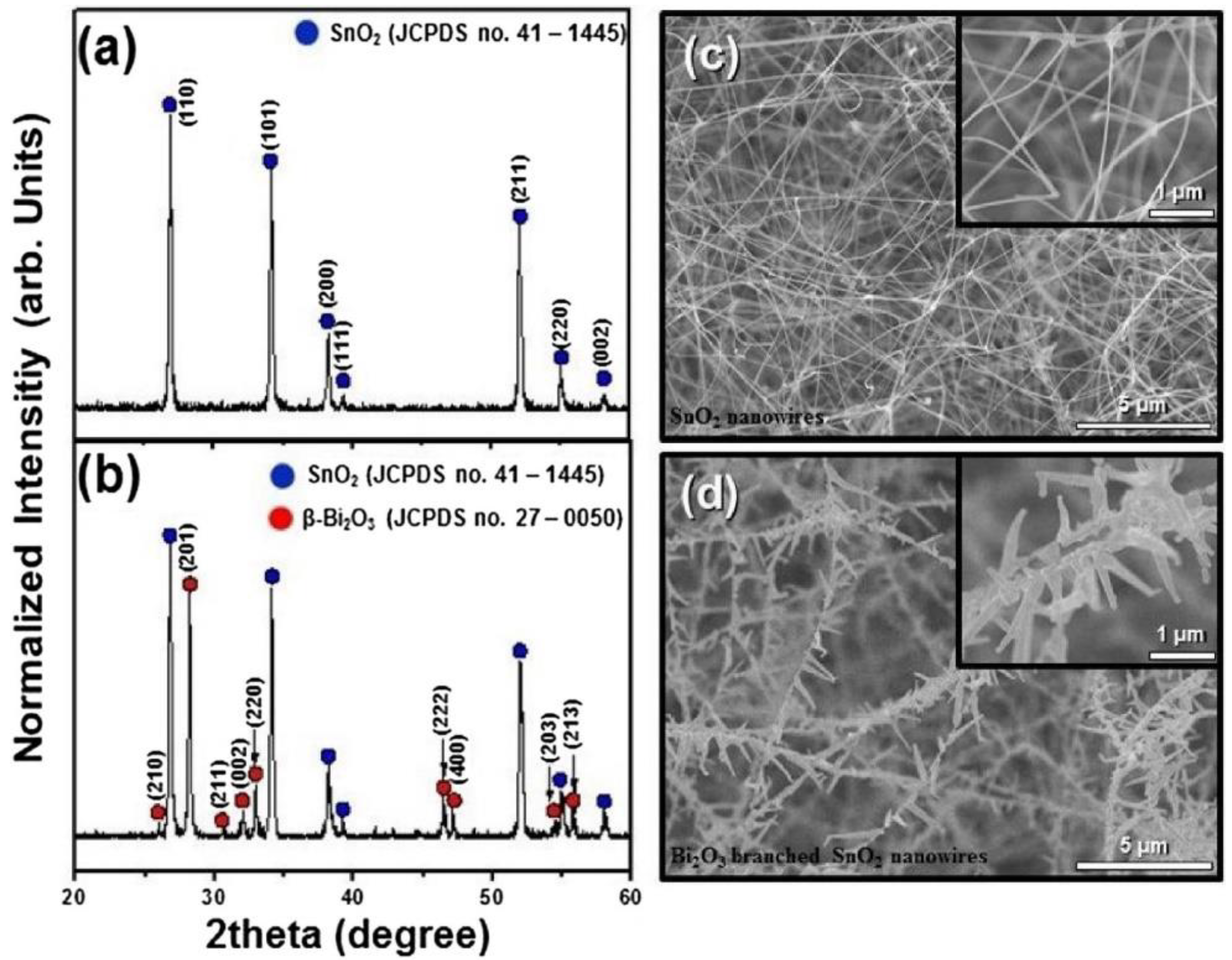
- Bang, J.H.; Choi, M.S.; Mirzaei, A.; Kwon, Y.J.; Kim, S.S.; Kim, T.W.; Kim, H.W. Selective NO2 sensor based on Bi2O3 branched SnO2 nanowires. Sens. Actuators B Chem. 2018, 274, 356–369. [Google Scholar] [CrossRef]
- Afshar, M.; Preiß, E.M.; Sauerwald, T.; Rodner, M.; Feili, D.; Straub, M.; König, K.; Schütze, A.; Seidel, H. Indium-tin-oxide single-nanowire gas sensor fabricated via laser writing and subsequent etching. Sens. Actuators B Chem. 2015, 215, 525–535. [Google Scholar] [CrossRef]
- Liao, L.; Mai, H.X.; Yuan, Q.; Lu, H.B.; Li, J.C.; Liu, C.; Yan, C.H.; Shen, Z.X.; Yu, T. Single CeO2 nanowire gas sensor supported with Pt nanocrystals: Gas sensitivity, surface bond states, and chemical mechanism. J. Phys. Chem. C 2008, 112, 9061–9065. [Google Scholar] [CrossRef]
- Tonezzer, M.; Hieu, N.V. Size-dependent response of single-nanowire gas sensors. Sens. Actuators B Chem. 2012, 163, 146–152. [Google Scholar] [CrossRef]
- Tonezzer, M. Selective gas sensor based on one single SnO2 nanowire. Sens. Actuators B Chem. 2019, 288, 53–59. [Google Scholar] [CrossRef]
- Czaban, J.A.; Thompson, D.A.; LaPierre, R.R. GaAs core−shell nanowires for photovoltaic applications. Nano Lett. 2009, 9, 148–154. [Google Scholar] [CrossRef]
- Kim, J.H.; Mirzaei, A.; Kim, H.W.; Kim, S.S. Variation of shell thickness in ZnO-SnO2 core-shell nanowires for optimizing sensing behaviors to CO, C6H6, and C7H8 gases. Sens. Actuators B-Chem. 2020, 302, 127150. [Google Scholar] [CrossRef]
- Xu, Y.; Tian, X.; Fan, Y.; Sun, Y. A formaldehyde gas sensor with improved gas response and sub-ppm level detection limit based on NiO/NiFe2O4 composite nanotetrahedrons. Sens. Actuators B Chem. 2020, 309, 127719. [Google Scholar] [CrossRef]
- Hwang, I.-S.; Kim, S.-J.; Choi, J.-K.; Choi, J.; Ji, H.; Kim, G.-T.; Cao, G.; Lee, J.-H. Synthesis and gas sensing characteristics of highly crystalline ZnO–SnO2 core–shell nanowires. Sens. Actuators B Chem. 2010, 148, 595–600. [Google Scholar] [CrossRef]
- Chen, I.; Lin, S.-S.; Lin, T.-J.; Hsu, C.-L.; Hsueh, T.J.; Shieh, T.-Y. The assessment for sensitivity of a NO2 gas sensor with ZnGa2O4/ZnO core-shell nanowires—A novel approach. Sensors 2010, 10, 3057–3072. [Google Scholar] [CrossRef] [PubMed]
- Park, S.; Hong, T.; Jung, J.; Lee, C. Room temperature hydrogen sensing of multiple networked ZnO/WO3 core–shell nanowire sensors under UV illumination. Curr. Appl. Phys. 2014, 14, 1171–1175. [Google Scholar] [CrossRef]
- Jang, Y.-G.; Kim, W.-S.; Kim, D.-H.; Hong, S.-H. Fabrication of Ga2O3/SnO2 core–shell nanowires and their ethanol gas sensing properties. J. Mater. Res. 2011, 26, 2322–2327. [Google Scholar] [CrossRef]
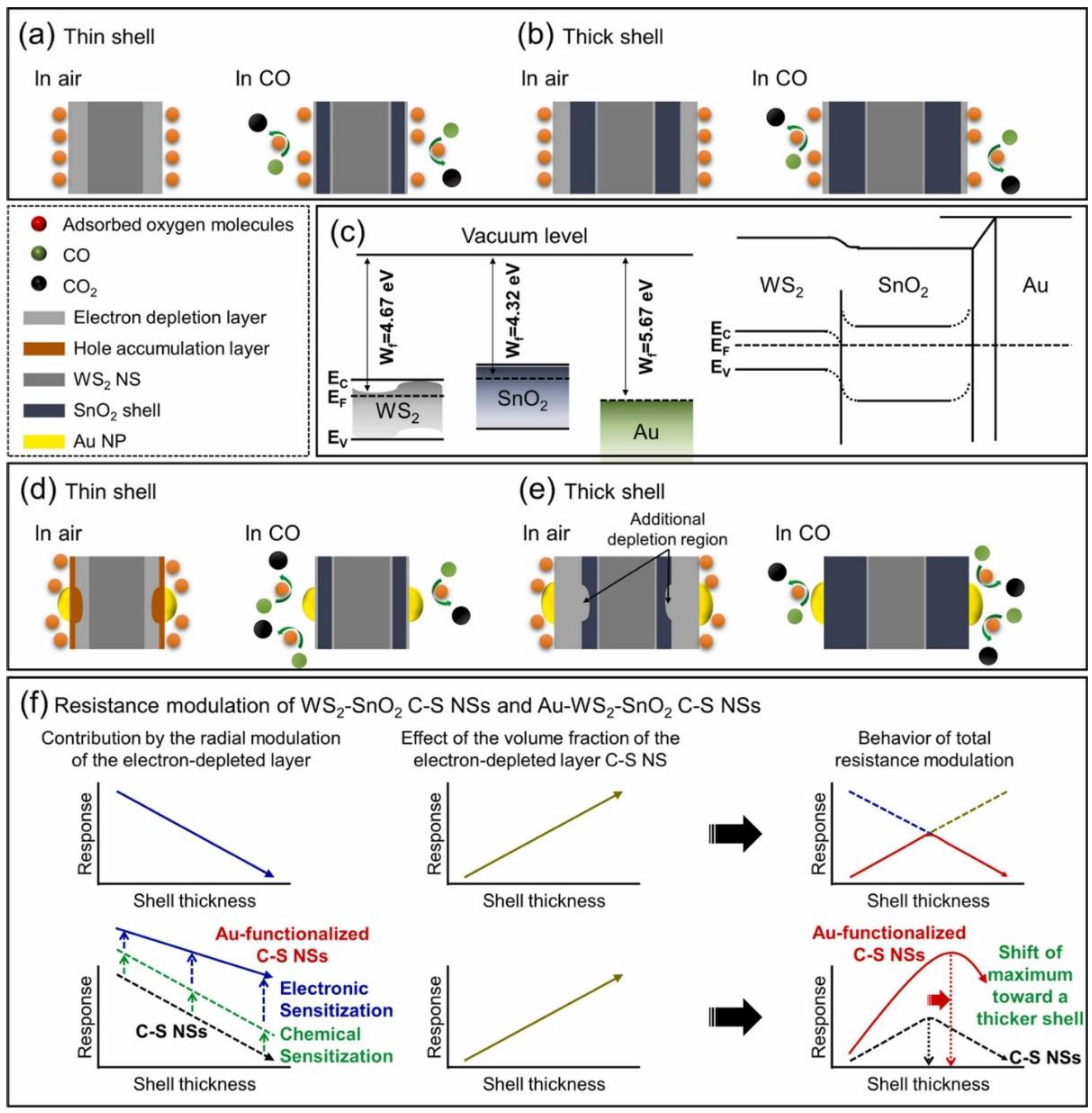
- Mirzaei, A.; Kim, J.-H.; Kim, H.W.; Kim, S.S. How shell thickness can affect the gas sensing properties of nanostructured materials: Survey of literature. Sens. Actuators B Chem. 2018, 258, 270–294. [Google Scholar] [CrossRef]
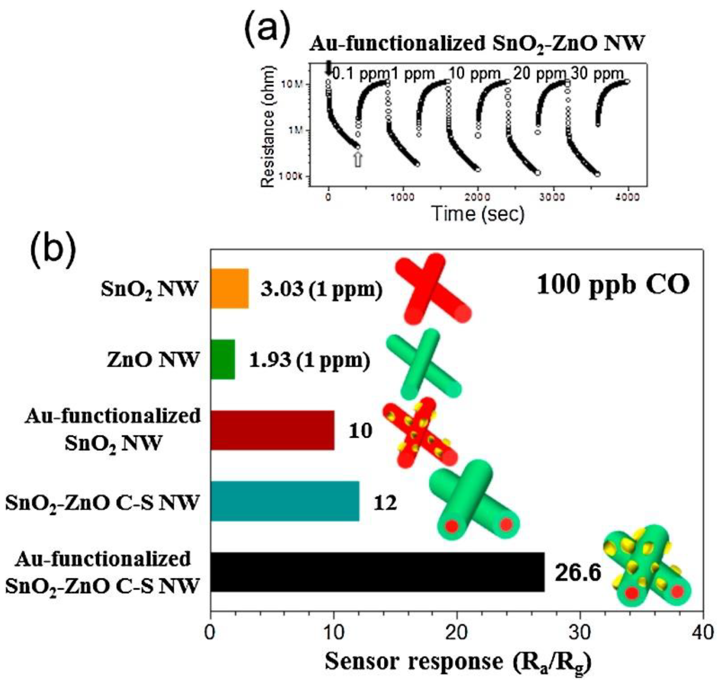
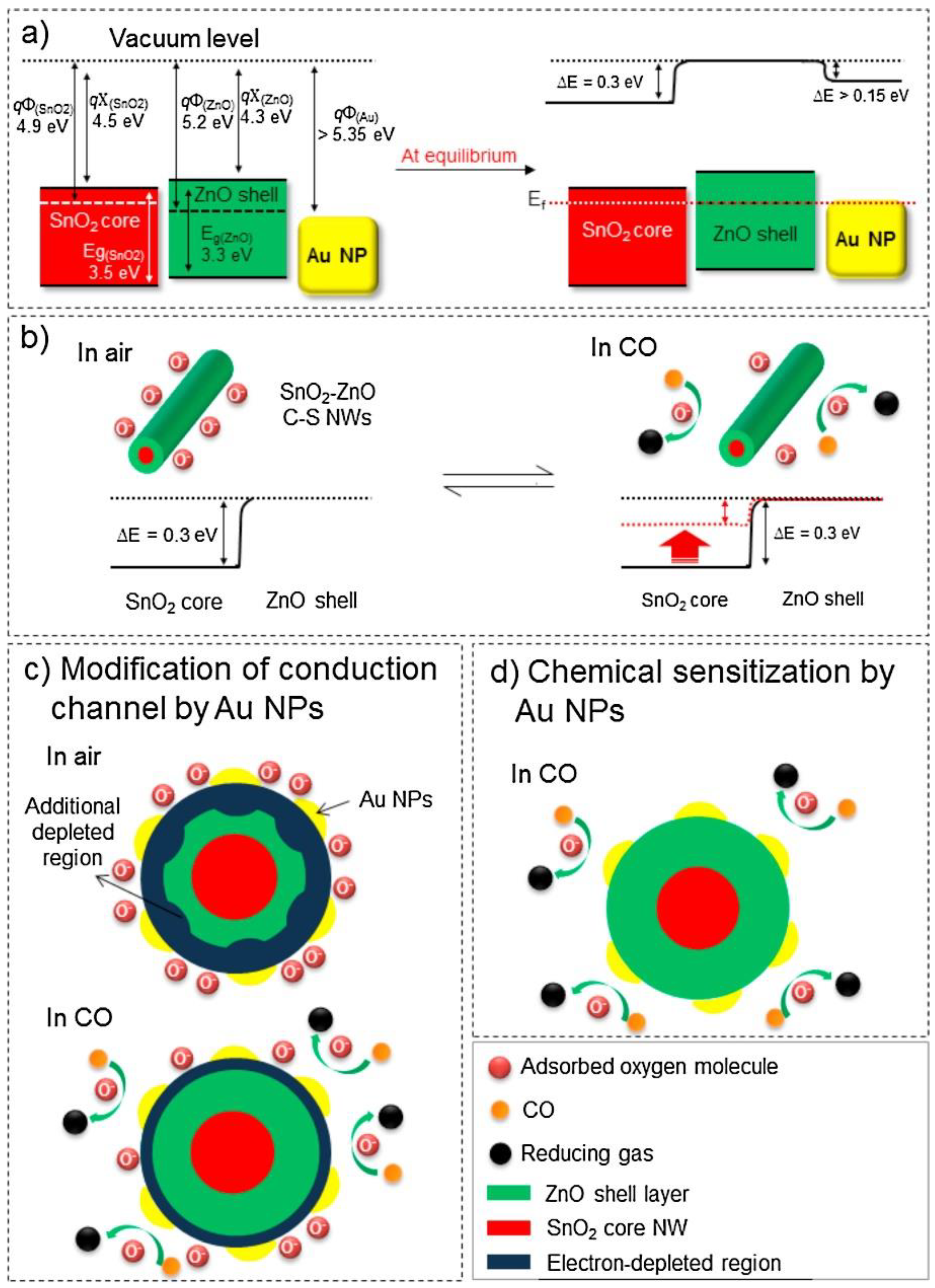
- Kim, J.H.; Mirzaei, A.; Kim, H.W.; Kim, S.S. Extremely sensitive and selective sub-ppm CO detection by the synergistic effect of Au nanoparticles and core–shell nanowires. Sens. Actuators B-Chem. 2017, 249, 177–188. [Google Scholar] [CrossRef]
- Salehi, A. A highly sensitive self heated SnO2 carbon monoxide sensor. Sens. Actuators B Chem. 2003, 96, 88–93. [Google Scholar] [CrossRef]
- Fàbrega, C.; Casals, O.; Hernández-Ramírez, F.; Prades, J.D. A review on efficient self-heating in nanowire sensors: Prospects for very-low power devices. Sens. Actuators B Chem. 2018, 256, 797–811. [Google Scholar] [CrossRef] [Green Version]
- Zhu, L.F.; She, J.C.; Luo, J.Y.; Deng, S.Z.; Chen, J.; Ji, X.W.; Xu, N.S. Self-heated hydrogen gas sensors based on Pt-coated W18O49 nanowire networks with high sensitivity, good selectivity and low power consumption. Sens. Actuators B Chem. 2011, 153, 354–360. [Google Scholar] [CrossRef]
- Majhi, S.M.; Mirzaei, A.; Kim, H.W.; Kim, S.S.; Kim, T.W. Recent advances in energy-saving chemiresistive gas sensors: A review. Nano Energy 2021, 79, 105369. [Google Scholar] [CrossRef]
- Ngoc, T.M.; Van Duy, N.; Hung, C.M.; Hoa, N.D.; Trung, N.N.; Nguyen, H.; Van Hieu, N. Ultralow power consumption gas sensor based on a self-heated nanojunction of SnO2 nanowires. RSC Adv. 2018, 8, 36323–36330. [Google Scholar] [CrossRef] [Green Version]
- Ngoc, T.M.; Van Duy, N.; Hoa, N.D.; Hung, C.M.; Nguyen, H.; Van Hieu, N. Effective design and fabrication of low-power-consumption self-heated SnO2 nanowire sensors for reducing gases. Sens. Actuators B Chem. 2019, 295, 144–152. [Google Scholar] [CrossRef]
- Ngoc, T.M.; Van Duy, N.; Hung, C.M.; Hoa, N.D.; Nguyen, H.; Tonezzer, M.; Van Hieu, N. Self-heated Ag-decorated SnO2 nanowires with low power consumption used as a predictive virtual multisensor for H2S-selective sensing. Anal. Chim. Acta 2019, 1069, 108–116. [Google Scholar] [CrossRef] [PubMed]
- Kim, J.-H.; Mirzaei, A.; Kim, H.W.; Kim, S.S. Low-voltage-driven sensors based on ZnO nanowires for room-temperature detection of NO2 and CO gases. ACS Appl. Mater. Interfaces 2019, 11, 24172–24183. [Google Scholar] [CrossRef] [PubMed]
- Kim, J.-H.; Mirzaei, A.; Bang, J.H.; Kim, H.W.; Kim, S.S. Selective H2S sensing without external heat by a synergy effect in self-heated CuO-functionalized SnO2-ZnO core-shell nanowires. Sens. Actuators B Chem. 2019, 300, 126981. [Google Scholar] [CrossRef]
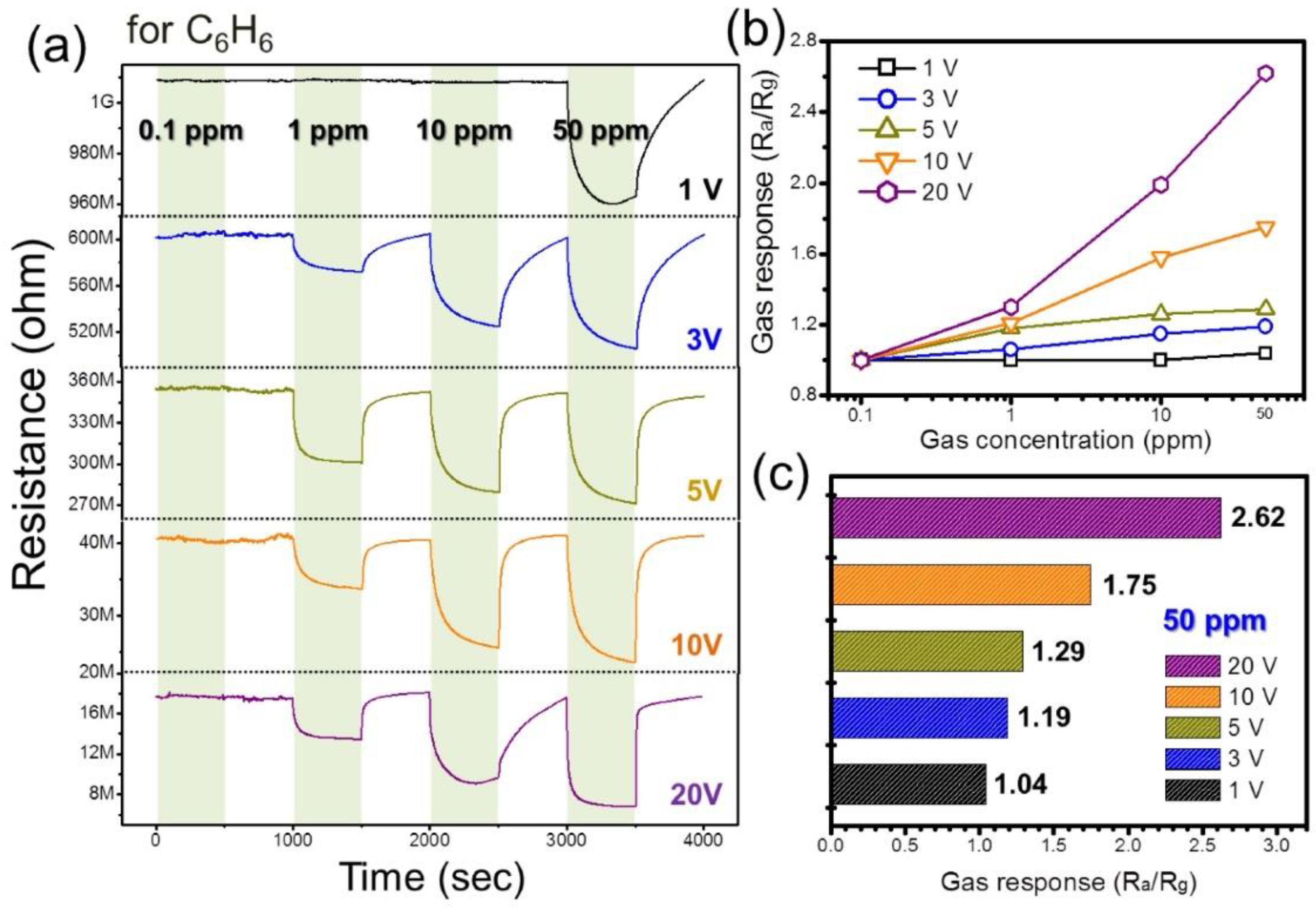
- Kim, J.-H.; Mirzaei, A.; Kim, H.W.; Kim, S.S. Pd-functionalized core-shell composite nanowires for self-heating, sensitive, and benzene-selective gas sensors. Sens. Actuators A Phys. 2020, 308, 112011. [Google Scholar] [CrossRef]
- Kou, X.; Xie, N.; Chen, F.; Wang, T.; Guo, L.; Wang, C.; Wang, Q.; Ma, J.; Sun, Y.; Zhang, H. Superior acetone gas sensor based on electrospun SnO2 nanofibers by Rh doping. Sens. Actuators B Chem. 2018, 256, 861–869. [Google Scholar] [CrossRef]
- Li, Y.; Zhu, J.; Cheng, H.; Li, G.; Cho, H.; Jiang, M.; Gao, Q.; Zhang, X. Developments of advanced electrospinning techniques: A critical review. Adv. Mater. Technol. 2021, 6, 2100410. [Google Scholar] [CrossRef]
- Rodríguez-Tobías, H.; Morales, G.; Grande, D. Comprehensive review on electrospinning techniques as versatile approaches toward antimicrobial biopolymeric composite fibers. Mater. Sci. Eng. C 2019, 101, 306–322. [Google Scholar] [CrossRef]
- Abideen, Z.U.; Kim, J.-H.; Lee, J.-H.; Kim, J.-Y.; Mirzaei, A.; Kim, H.W.; Kim, S.S. Electrospun metal oxide composite nanofibers gas sensors: A review. J. Korean Ceram. Soc. 2017, 54, 366–379. [Google Scholar] [CrossRef] [Green Version]
- Islam, M.S.; Ang, B.C.; Andriyana, A.; Afifi, A.M. A review on fabrication of nanofibers via electrospinning and their applications. SN Appl. Sci. 2019, 1, 1–16. [Google Scholar] [CrossRef] [Green Version]
- Haider, A.; Haider, S.; Kang, I.-K. A comprehensive review summarizing the effect of electrospinning parameters and potential applications of nanofibers in biomedical and biotechnology. Arab. J. Chem. 2018, 11, 1165–1188. [Google Scholar] [CrossRef]
- Tsai, P.; Chen, J.; Ercan, E.; Chueh, C.; Tung, S.; Chen, W. Uniform luminous perovskite nanofibers with color-tunability and improved stability prepared by one-step core/shell electrospinning. Small 2018, 14, 1704379. [Google Scholar] [CrossRef]
- Huang, B.; Zhang, Z.; Zhao, C.; Cairang, L.; Bai, J.; Zhang, Y.; Mu, X.; Du, J.; Wang, H.; Pan, X. Enhanced gas-sensing performance of ZnO@ In2O3 core@ shell nanofibers prepared by coaxial electrospinning. Sens. Actuators B Chem. 2018, 255, 2248–2257. [Google Scholar] [CrossRef]
- Ding, B.; Wang, M.; Yu, J.; Sun, G. Gas sensors based on electrospun nanofibers. Sensors 2009, 9, 1609–1624. [Google Scholar] [CrossRef] [PubMed] [Green Version]
- Kim, J.H.; Lee, J.H.; Kim, J.Y.; Mirzaei, A.; Kim, H.W.; Kim, S.S. Enhancement of CO and NO2 sensing in n-SnO2-p-Cu2O core-shell nanofibers by shell optimization. J. Hazard. Mater. 2019, 376, 68–82. [Google Scholar] [CrossRef] [PubMed]
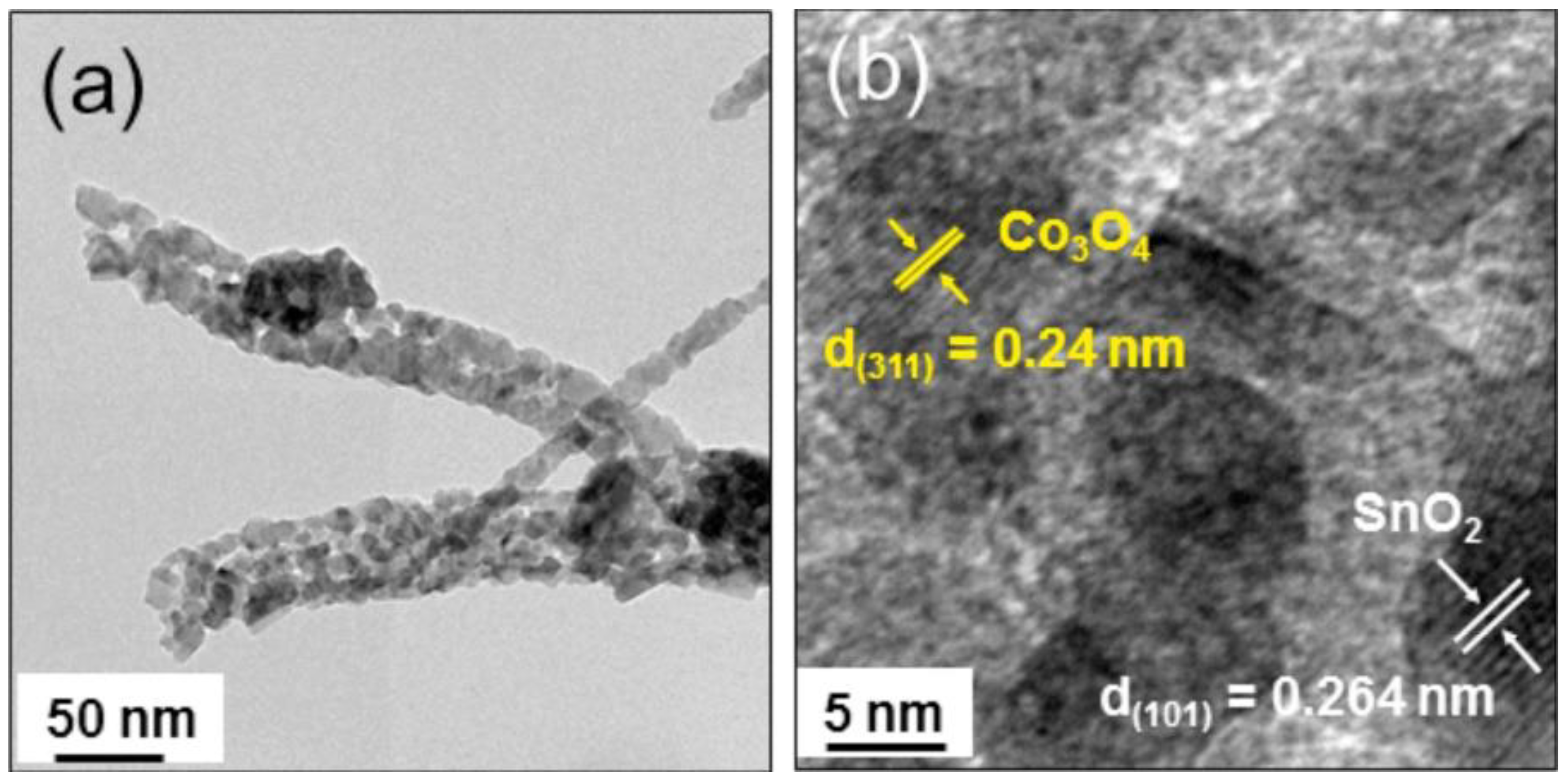
- Kim, J.-H.; Lee, J.-H.; Mirzaei, A.; Kim, H.W.; Kim, S.S. Optimization and gas sensing mechanism of n-SnO2-p-Co3O4 composite nanofibers. Sens. Actuators B Chem. 2017, 248, 500–511. [Google Scholar] [CrossRef]
- Lim, S.K.; Hwang, S.-H.; Chang, D.; Kim, S. Preparation of mesoporous In2O3 nanofibers by electrospinning and their application as a CO gas sensor. Sens. Actuators B Chem. 2010, 149, 28–33. [Google Scholar] [CrossRef]
- Liu, L.; Zhang, Y.; Wang, G.; Li, S.; Wang, L.; Han, Y.; Jiang, X.; Wei, A. High toluene sensing properties of NiO–SnO2 composite nanofiber sensors operating at 330 °C. Sens. Actuators B Chem. 2011, 160, 448–454. [Google Scholar] [CrossRef]
- Im, D.; Kim, D.; Jeong, D.; Park, W.I.; Chun, M.; Park, J.-S.; Kim, H.; Jung, H. Improved formaldehyde gas sensing properties of well-controlled Au nanoparticle-decorated In2O3 nanofibers integrated on low power MEMS platform. J. Mater. Sci. Technol. 2020, 38, 56–63. [Google Scholar] [CrossRef]
- Lin, Y.; Wei, W.; Li, Y.; Li, F.; Zhou, J.; Sun, D.; Chen, Y.; Ruan, S. Preparation of Pd nanoparticle-decorated hollow SnO2 nanofibers and their enhanced formaldehyde sensing properties. J. Alloys Compd. 2015, 651, 690–698. [Google Scholar] [CrossRef]
- Gao, X.; Li, F.; Wang, R.; Zhang, T. A formaldehyde sensor: Significant role of pn heterojunction in gas-sensitive core-shell nanofibers. Sens. Actuators B Chem. 2018, 258, 1230–1241. [Google Scholar] [CrossRef]
- Majhi, S.M.; Mirzaei, A.; Kim, H.W.; Kim, S.S. Reduced graphene oxide (rGO)-loaded metal-oxide nanofiber gas sensors: An overview. Sensors 2021, 21, 1352. [Google Scholar] [CrossRef]
- Cho, I.; Kang, K.; Yang, D.; Yun, J.; Park, I. Localized liquid-phase synthesis of porous SnO2 nanotubes on MEMS platform for low-power, high performance gas sensors. ACS Appl. Mater. Interfaces 2017, 9, 27111–27119. [Google Scholar] [CrossRef] [Green Version]
- Jankiewicz, B.J.; Jamiola, D.; Choma, J.; Jaroniec, M. Silica–metal core–shell nanostructures. Adv. Colloid Interface Sci. 2012, 170, 28–47. [Google Scholar] [CrossRef]
- Lee, J.-H. Gas sensors using hierarchical and hollow oxide nanostructures: Overview. Sens. Actuators B Chem. 2009, 140, 319–336. [Google Scholar] [CrossRef]
- Choi, H.-J.; Kwon, S.-H.; Lee, W.-S.; Im, K.-G.; Kim, T.-H.; Noh, B.-R.; Park, S.; Oh, S.; Kim, K.-K. Ultraviolet photoactivated room temperature NO2 gas sensor of ZnO hemitubes and nanotubes covered with TiO2 nanoparticles. Nanomaterials 2020, 10, 462. [Google Scholar] [CrossRef] [Green Version]
- Hazra, A.; Bhowmik, B.; Dutta, K.; Chattopadhyay, P.P.; Bhattacharyya, P. Stoichiometry, length, and wall thickness optimization of TiO2 nanotube array for efficient alcohol sensing. ACS Appl. Mater. Interfaces 2015, 7, 9336–9348. [Google Scholar] [CrossRef]
- Liu, F.-T.; Gao, S.-F.; Pei, S.-K.; Tseng, S.-C.; Liu, C.-H.J. ZnO nanorod gas sensor for NO2 detection. J. Taiwan Inst. Chem. Eng. 2009, 40, 528–532. [Google Scholar] [CrossRef]
- Rai, P.; Song, H.-M.; Kim, Y.-S.; Song, M.-K.; Oh, P.-R.; Yoon, J.-M.; Yu, Y.-T. Microwave assisted hydrothermal synthesis of single crystalline ZnO nanorods for gas sensor application. Mater. Lett. 2012, 68, 90–93. [Google Scholar] [CrossRef]
- Wei, Y.; Hu, M.; Yan, W.; Wang, D.; Yuan, L.; Qin, Y. Hydrothermal synthesis porous silicon/tungsten oxide nanorods composites and their gas-sensing properties to NO2 at room temperature. Appl. Surf. Sci. 2015, 353, 79–86. [Google Scholar] [CrossRef]
- Da Silva, L.F.; Catto, A.C.; Avansi, W., Jr.; Cavalcante, L.S.; Mastelaro, V.R.; Andres, J.; Aguir, K.; Longo, E. Acetone gas sensor based on α-Ag2WO4 nanorods obtained via a microwave-assisted hydrothermal route. J. Alloys Compd. 2016, 683, 186–190. [Google Scholar] [CrossRef] [Green Version]
- Zhang, H.; Feng, J.; Wang, J.; Zhang, M. Preparation of ZnO nanorods through wet chemical method. Mater. Lett. 2007, 61, 5202–5205. [Google Scholar] [CrossRef]
- Liu, Y.; Liu, M. Ordered ZnO nanorods synthesized by combustion chemical vapor deposition. J. Nanosci. Nanotechnol. 2007, 7, 4529–4533. [Google Scholar] [CrossRef]
- Chien, F.S.-S.; Wang, C.-R.; Chan, Y.-L.; Lin, H.-L.; Chen, M.-H.; Wu, R.-J. Fast-response ozone sensor with ZnO nanorods grown by chemical vapor deposition. Sens. Actuators B Chem. 2010, 144, 120–125. [Google Scholar] [CrossRef]
- Cha, H.G.; Kim, C.W.; Kim, Y.H.; Jung, M.H.; Ji, E.S.; Das, B.K.; Kim, J.C.; Kang, Y.S. Preparation and characterization of α-Fe2O3 nanorod-thin film by metal–organic chemical vapor deposition. Thin Solid Film. 2009, 517, 1853–1856. [Google Scholar] [CrossRef]
- Pradhan, S.K.; Reucroft, P.J.; Yang, F.; Dozier, A. Growth of TiO2 nanorods by metalorganic chemical vapor deposition. J. Cryst. Growth 2003, 256, 83–88. [Google Scholar] [CrossRef]
- Liu, B.; Hu, Z.; Che, Y.; Allenic, A.; Sun, K.; Pan, X. Growth of ZnO nanoparticles and nanorods with ultrafast pulsed laser deposition. Appl. Phys. A 2008, 93, 813–818. [Google Scholar] [CrossRef]
- Yang, T.; Yu, H.; Xiao, B.; Li, Z.; Zhang, M. Enhanced 1-butylamine gas sensing characteristics of flower-like V2O5 hierarchical architectures. J. Alloys Compd. 2017, 699, 921–927. [Google Scholar] [CrossRef] [Green Version]
- Sik, C.M.; Young, K.M.; Mirzaei, A.; Kim, H.-S.; Kim, S.-I.; Baek, S.-H.; Won, C.D.; Jin, C.; Hyoung, L.K. Selective, sensitive, and stable NO2 gas sensor based on porous ZnO nanosheets. Appl. Surf. Sci. 2021, 568, 150910. [Google Scholar]
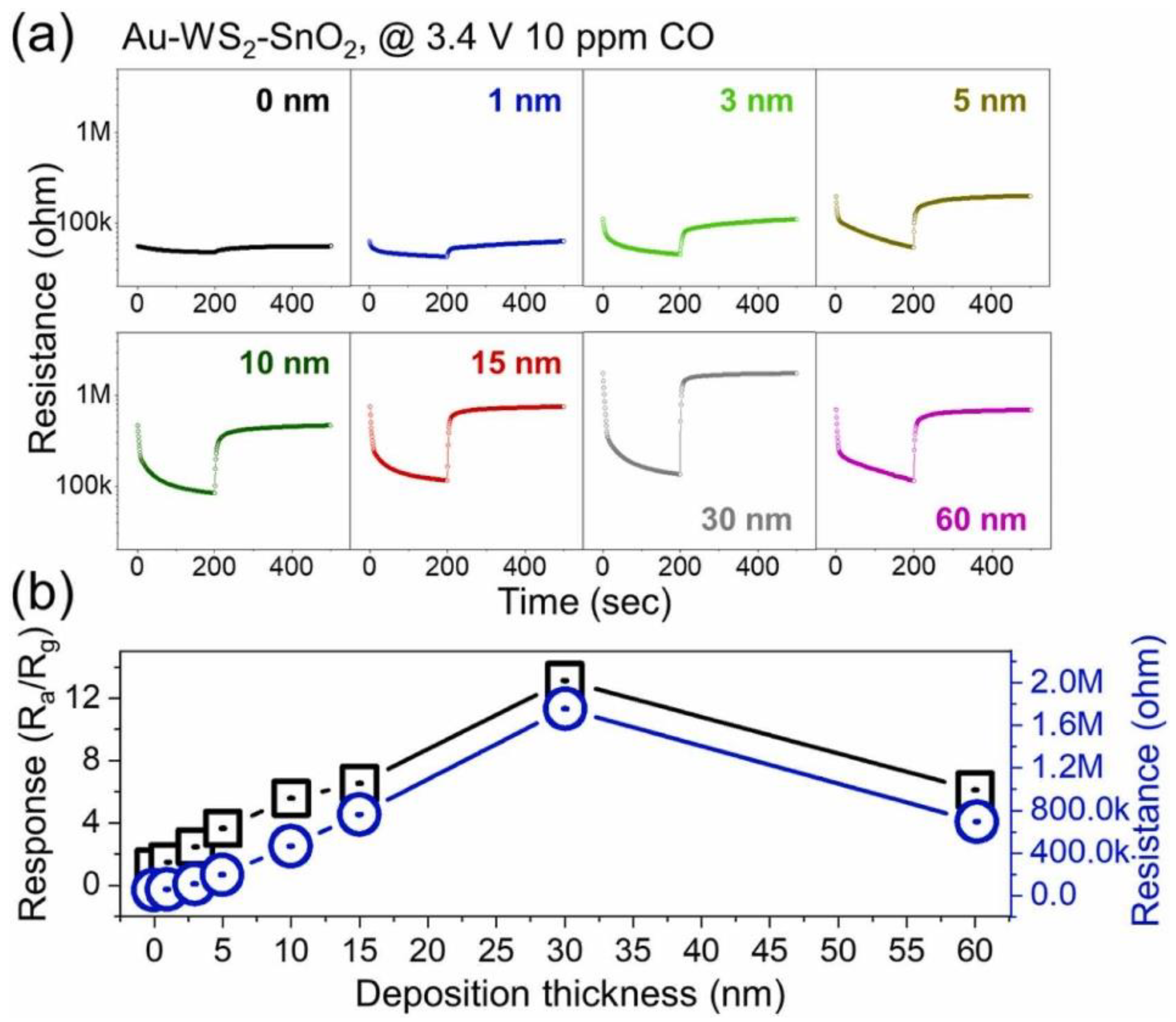
- Kim, J.-H.; Mirzaei, A.; Kim, J.-Y.; Yang, D.-H.; Kim, S.S.; Kim, H.W. Selective CO gas sensing by Au-decorated WS2-SnO2 core-shell nanosheets on flexible substrates in self-heating mode. Sens. Actuators B Chem. 2022, 353, 131197. [Google Scholar] [CrossRef]
- Xia, Y.; Wang, J.; Chen, R.; Zhou, D.; Xiang, L. A review on the fabrication of hierarchical ZnO nanostructures for photocatalysis application. Crystals 2016, 6, 148. [Google Scholar] [CrossRef]
- Liu, J.; Zhang, L.; Fan, J.; Zhu, B.; Yu, J. Triethylamine gas sensor based on Pt-functionalized hierarchical ZnO microspheres. Sens. Actuators B-Chem. 2021, 331, 129425. [Google Scholar] [CrossRef]
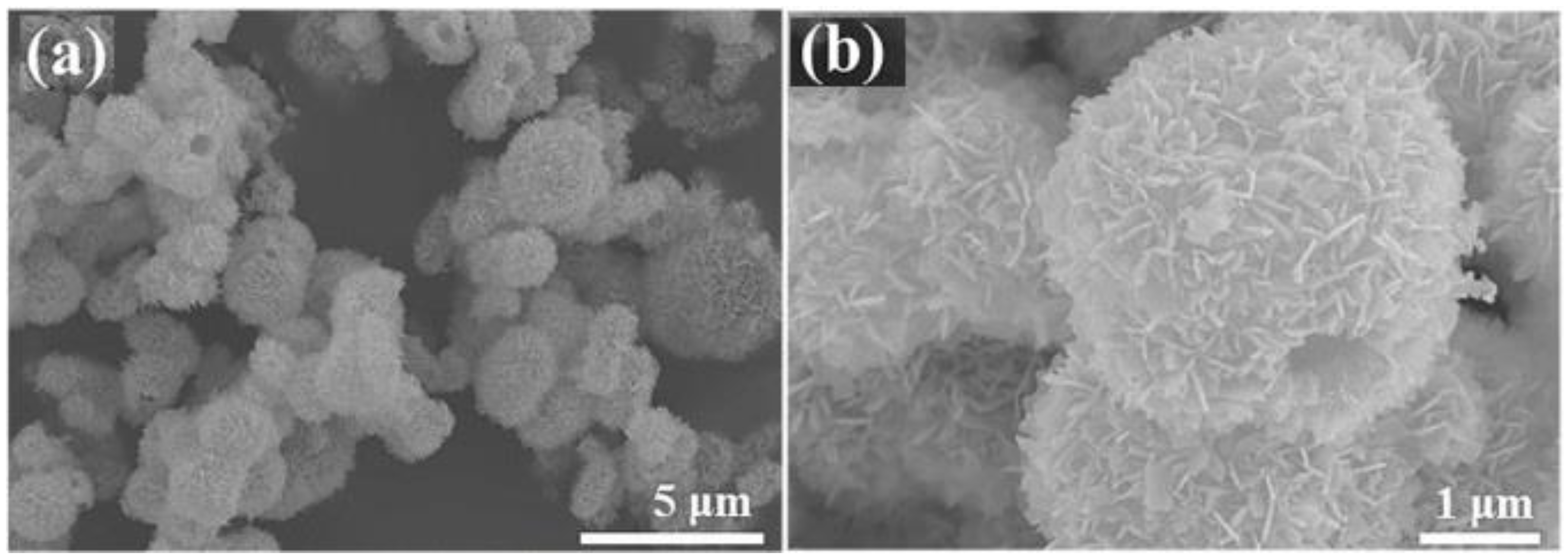
- Cheng, P.; Dang, F.; Wang, Y.; Gao, J.; Xu, L.; Wang, C.; Lv, L.; Li, X.; Zhang, B.; Liu, B. Gas sensor towards n-butanol at low temperature detection: Hierarchical flower-like Ni-doped Co3O4 based on solvent-dependent synthesis. Sens. Actuators B-Chem. 2021, 328, 129028. [Google Scholar] [CrossRef]
- Guo, M.; Luo, N.; Chen, Y.; Fan, Y.; Wang, X.; Xu, J. Fast-response MEMS xylene gas sensor based on CuO/WO3 hierarchical structure. J. Hazard. Mater. 2022, 429, 127471. [Google Scholar] [CrossRef]
- Yu, H.; Guo, C.; Zhang, X.; Xu, Y.; Cheng, X.; Gao, S.; Huo, L. Recent Development of Hierarchical Metal Oxides Based Gas Sensors: From Gas Sensing Performance to Applications. Adv. Sustain. Syst. 2022, 6, 2100370. [Google Scholar] [CrossRef]
- Mirzaei, A.; Janghorban, K.; Hashemi, B.; Neri, G. Metal-core@metal oxide-shell nanomaterials for gas-sensing applications: A review. J. Nanoparticle Res. 2015, 17, 371. [Google Scholar] [CrossRef]
- Yamazoe, N. New approaches for improving semiconductor gas sensors. Sens. Actuators B Chem. 1991, 5, 7–19. [Google Scholar] [CrossRef]
- Mirzaei, A.; Yousefi, H.R.; Falsafi, F.; Bonyani, M.; Lee, J.-H.; Kim, J.-H.; Kim, H.W.; Kim, S.S. An overview on how Pd on resistive-based nanomaterial gas sensors can enhance response toward hydrogen gas. Int. J. Hydrogen Energy 2019, 44, 20552–20571. [Google Scholar] [CrossRef]
- Iordache, S.M.; Ionete, E.I.; Iordache, A.M.; Tanasa, E.; Stamatin, I.; Grigorescu, C.E.A. Pd-decorated CNT as sensitive material for applications in hydrogen isotopes sensing-Application as gas sensor. Int. J. Hydrogen Energy 2021, 46, 11015–11024. [Google Scholar] [CrossRef]
- Li, G.; Fan, Y.; Hu, Q.; Zhang, D.; Ma, Z.; Cheng, Z.; Wang, X.; Xu, J. Morphology and size effect of Pd nanocrystals on formaldehyde and hydrogen sensing performance of SnO2 based gas sensor. J. Alloys Compd. 2022, 906, 163765. [Google Scholar] [CrossRef]
- Shen, S.-K.; Cui, X.-L.; Guo, C.-Y.; Dong, X.; Zhang, X.-F.; Cheng, X.-L.; Huo, L.-H.; Xu, Y.-M. Sensing mechanism of Ag/α-MoO3 nanobelts for H2S gas sensor. Rare Met. 2021, 40, 1545–1553. [Google Scholar] [CrossRef]
- Kim, J.-H.; Kim, S.S. Realization of ppb-scale toluene-sensing abilities with Pt-functionalized SnO2–ZnO core–shell nanowires. ACS Appl. Mater. Interfaces 2015, 7, 17199–17208. [Google Scholar] [CrossRef]
- Kim, J.-H.; Wu, P.; Kim, H.W.; Kim, S.S. Highly selective sensing of CO, C6H6, and C7H8 gases by catalytic functionalization with metal nanoparticles. ACS Appl. Mater. Interfaces 2016, 8, 7173–7183. [Google Scholar] [CrossRef]
- Li, X.; Yu, J.; Wageh, S.; Al-Ghamdi, A.A.; Xie, J. Graphene in photocatalysis: A review. Small 2016, 12, 6640–6696. [Google Scholar] [CrossRef]
- Schedin, F.; Geim, A.K.; Morozov, S.V.; Hill, E.W.; Blake, P.; Katsnelson, M.I.; Novoselov, K.S. Detection of individual gas molecules adsorbed on graphene. Nat. Mater. 2007, 6, 652–655. [Google Scholar] [CrossRef]
- Chatterjee, S.G.; Chatterjee, S.; Ray, A.K.; Chakraborty, A.K. Graphene–metal oxide nanohybrids for toxic gas sensor: A review. Sens. Actuators B Chem. 2015, 221, 1170–1181. [Google Scholar] [CrossRef]
- Pendolino, F.; Armata, N. Graphene Oxide in Environmental Remediation Process; Springer: Berlin/Heidelberg, Germany, 2017; Volume 11. [Google Scholar]
- Hummers, W.S., Jr.; Offeman, R.E. Preparation of graphitic oxide. J. Am. Chem. Soc. 1958, 80, 1339. [Google Scholar] [CrossRef]
- Brodie, B.C. Hydration behavior and dynamics of water molecules in graphite oxide. Ann. Chim Phys. 1860, 59, 466–472. [Google Scholar]
- Shewale, P.S.; Yun, K.-S. Synthesis and characterization of Cu-doped ZnO/RGO nanocomposites for room-temperature H2S gas sensor. J. Alloys Compd. 2020, 837, 155527. [Google Scholar] [CrossRef]
- Liu, Z.; Yu, L.; Guo, F.; Liu, S.; Qi, L.; Shan, M.; Fan, X. Facial development of high performance room temperature NO2 gas sensors based on ZnO nanowalls decorated rGO nanosheets. Appl. Surf. Sci. 2017, 423, 721–727. [Google Scholar] [CrossRef]
- Jia, A.; Liu, B.; Liu, H.; Li, Q.; Yun, Y. Interface design of SnO2@PANI nanotube with enhanced sensing performance for ammonia detection at room temperature. Front. Chem. 2020, 8, 383. [Google Scholar] [CrossRef]
- Amiri, V.; Roshan, H.; Mirzaei, A.; Neri, G.; Ayesh, A.I. Nanostructured metal oxide-based acetone gas sensors: A review. Sensors 2020, 20, 3096. [Google Scholar] [CrossRef]
- Sharma, H.J.; Salorkar, M.A.; Kondawar, S.B. H2 and CO gas sensor from SnO2/polyaniline composite nanofibers fabricated by electrospinning. Adv. Mater. Proc. 2017, 2, 61–66. [Google Scholar] [CrossRef] [Green Version]


| Property | Pt | Pd | Au | Ag |
|---|---|---|---|---|
| Melting point (°C) | 1769 | 1552 | 1064.4 | 961.9 |
| Atomic number | 78 | 46 | 79 | 47 |
| Atomic mass (g/mol) | 195.09 | 160.4 | 196.97 | 107.86 |
| Density (g/cm3) | 21.45 | 12.02 | 19.30 | 10.49 |
| Work function (eV) | ~5.65 | ~5.3 | ~5.1 | ~4.3 |
| Electron negativity | 2.2 | 2.2 | 2.4 | 1.9 |
| Sensing Material | Morphology | Gas | Conc. (ppm) | T | Response (Ra/Rg) or (Rg/Ra) | Ref. |
|---|---|---|---|---|---|---|
| TiO2/SnO2 | QD | NO2 | 1 | 300 | 2.62 | [25] |
| SnO2 | QD | C4H10 | 8219.2 | 25 | 8.09 | [26] |
| SnO2 | QD | C2H5OH | 300 | N/A * | 215 | [27] |
| Pt-SnO2 | NW | C7H8 | 100 | 300 | 55 | [32] |
| In2O3/SnO2 | NW | NO2 | 5 | 300 | 25 | [34] |
| In2O3 | NR | CO | 400 | 350 | 3.5 | [35] |
| SnO2 | NW | NO2 | 5 | 200 | 180 | [36] |
| SnO2 | NW | LPG | 2000 | 350 | 21.8 | [37] |
| SnO2 | NW | H2 | 1000 | 300 | 3.3 | [42] |
| ZnO | NW | NO2 | 20 | 225 | 95 | [43] |
| SnO2 | NW | C2H5OH | 100 | 300 | 50.6 | [48] |
| ZnO | NW | NO2 | 5 | 300 | 106 | [49] |
| ZnO-SnO2 | NR | C2H5OH | 100 | 275 | 18 | [50] |
| Ni/ZnO | NW | p-xylene | 5 | 400 | 42.44 | [52] |
| Gr/ZnO | NW | C2H5OH | 20 | 125 | 23 | [53] |
| Bi2O3/SnO2 | NW | NO2 | 2 | 250 | 56.92 | [54] |
| Pt/CeO2 | NW | CO | 200 | 25 | 3 | [56] |
| SnO2 | NW | NO2 | 500 | 300 | 17 | [57] |
| SnO2 | NW | C2H5OH | 50 | 350 | 6.7 | [58] |
| NiO/NiFe2O4 | Nanotetrahedrons | HCHO | 50 | 240 | 19 | [61] |
| ZnO/SnO2 | NW | C2H5OH | 200 | 400 | 280 | [62] |
| ZnGa2O4/ZnO | NW | NO2 | 10 | 250 | 23 | [63] |
| ZnO/WO3 | NW | H2 | 1000 | 25 | 6.45 | [64] |
| Ga2O3/SnO2 | NW | C2H5OH | 1000 | 400 | 66 | [65] |
| Au/SnO2–ZnO | NW | CO | 0.1 | 300 | 26.6 | [67] |
| Pt/W18O49 | NW | H2 | 1000 | 200 | 0.528 | [70] |
| Ag/SnO2 | NW | H2S | 0.5 | N/A * | 21.2 | [73] |
| Rh/SnO2 | NF | C3H6O | 50 | 200 | 60.6 | [78] |
| ZnO/In2O3 | NF | C2H5OH | 100 | 225 | 31.87 | [85] |
| SnO2/Cu2O | NF | NO2 | 10 | 300 | 5 | [87] |
| In2O3 | NF | CO | 100 | 300 | 5.4 | [89] |
| Pd/SnO2 | NF | HCHO | 100 | 160 | 18.8 | [92] |
| Co3O4/ZnO | NF | HCHO | 100 | 220 | 5 | [93] |
| TiO2/ZnO | Hemitube | NO2 | 25 | 25 | 1.23 | [98] |
| ZnO | NR | NO2 | 5 | 250 | 200 | [100] |
| ZnO | NR | C2H5OH | 250 | 400 | 7 | [101] |
| α-Ag2WO4 | NR | C3H6O | 20 | 350 | 3.6 | [103] |
| ZnO | NR | O3 | 2.5 | 575 | 850 | [106] |
| ZnO | NS | NO2 | 10 | 200 | 74.68 | [111] |
Publisher’s Note: MDPI stays neutral with regard to jurisdictional claims in published maps and institutional affiliations. |
© 2022 by the authors. Licensee MDPI, Basel, Switzerland. This article is an open access article distributed under the terms and conditions of the Creative Commons Attribution (CC BY) license (https://creativecommons.org/licenses/by/4.0/).
Share and Cite
Mirzaei, A.; Ansari, H.R.; Shahbaz, M.; Kim, J.-Y.; Kim, H.W.; Kim, S.S. Metal Oxide Semiconductor Nanostructure Gas Sensors with Different Morphologies. Chemosensors 2022, 10, 289. https://doi.org/10.3390/chemosensors10070289
Mirzaei A, Ansari HR, Shahbaz M, Kim J-Y, Kim HW, Kim SS. Metal Oxide Semiconductor Nanostructure Gas Sensors with Different Morphologies. Chemosensors. 2022; 10(7):289. https://doi.org/10.3390/chemosensors10070289
Chicago/Turabian StyleMirzaei, Ali, Hamid Reza Ansari, Mehrdad Shahbaz, Jin-Young Kim, Hyoun Woo Kim, and Sang Sub Kim. 2022. "Metal Oxide Semiconductor Nanostructure Gas Sensors with Different Morphologies" Chemosensors 10, no. 7: 289. https://doi.org/10.3390/chemosensors10070289