Article

State Feedback with Integral Control Circuit Design of DC-DC Buck-Boost Converter

by
Humam Al-Baidhani
1,2,
Abdullah Sahib
3 and
Marian K. Kazimierczuk
1,*
1
Department of Electrical Engineering, Wright State University, Dayton, OH 45435, USA
2
Department of Computer Techniques Engineering, Faculty of Information Technology, Imam Ja’afar Al-Sadiq University, Baghdad 10011, Iraq
3
Department of Electronic and Communication Technologies, Technical Institute, Al-Furat Al-Awsat Technical University, Najaf 54003, Iraq
*
Author to whom correspondence should be addressed.
Mathematics 2023, 11(9), 2139; https://doi.org/10.3390/math11092139
Submission received: 31 March 2023 / Revised: 27 April 2023 / Accepted: 28 April 2023 / Published: 3 May 2023
(This article belongs to the Special Issue Dynamic Modeling and Simulation for Control Systems, 2nd Edition)

Abstract

:
The pulse-with modulated (PWM) dc-dc buck-boost converter is a non-minimum phase system, which requires a proper control scheme to improve the transient response and provide constant output voltage during line and load variations. The pole placement technique has been proposed in the literature to control this type of power converter and achieve the desired response. However, the systematic design procedure of such control law using a low-cost electronic circuit has not been discussed. In this paper, the pole placement via state-feedback with an integral control scheme of inverting the PWM dc-dc buck-boost converter is introduced. The control law is developed based on the linearized power converter model in continuous conduction mode. A detailed design procedure is given to represent the control equation using a simple electronic circuit that is suitable for low-cost commercial applications. The mathematical model of the closed-loop power converter circuit is built and simulated using SIMULINK and Simscape Electrical in MATLAB. The closed-loop dc-dc buck-boost converter is tested under various operating conditions. It is confirmed that the proposed control scheme improves the power converter dynamics, tracks the reference signal, and maintains regulated output voltage during abrupt changes in input voltage and load current. The simulation results show that the line variation of 5 V and load variation of 2 A around the nominal operating point are rejected with a maximum percentage overshoot of 3.5% and a settling time of 5.5 ms.

1. Introduction

The PWM dc-dc converters are utilized in modern aircraft power systems and portable communication devices due to their high efficiency, small size, and low cost. Portable electronic devices such as cell phones and laptops require a well-regulated dc supply voltage to operate properly. However, the dc-dc converters encounter line and load variations during their normal operation, which fluctuate the load voltage. Therefore, a controller is required to provide a constant voltage and improve the transient response of the power converter. Modern control techniques have been applied to control the power converter dynamics due to their robustness against large disturbances. In [1], neural inverse optimal control (NIOC) for a regenerative braking system in an electric vehicle (EV). A neural identifier has been trained with an extended Kalman filter (EKF) to estimate the dc-dc buck-boost power converter dynamics. An artificial neural network-based controller has also been developed for a bidirectional power flow management system that comprises a dual-source low-voltage buck-boost converter [2]. However, the practical implementation of the control schemes in [1,2] is complicated.
Other research efforts have proposed model predictive control (MPC) and adaptive control techniques as alternatives for artificial neural network-based controllers. For instance, the MPC of the buck-boost converter has been introduced in [3], in which a switching algorithm is proposed to minimize the error for the power converter. In [4], a centralized model predictive control has been developed to stabilize the DC microgrid with versatile buck-boost converters. A direct model reference adaptive control [5] and an optimal adaptive control [6] have also been presented for boost and voltage source converters, respectively. A nonlinear control based on the Lyapunov function has been developed in [7] for power management systems, whereas an inverse-system decoupling control method has been presented in [8] for a dc-dc buck-boost converter. Despite the robust control performance, the previous control strategies require tedious mathematical computations and high-cost for practical implementation.
Feedback linearization methods have been discussed in [9,10,11,12,13] for dc-dc power converters. A feedback control law based on full feedback linearization has been introduced for the buck, boost, and buck-boost converters [9]. Feedback linearization has been presented to control the buck-boost power converter [10,11], boost converter [12], and modular multilevel converter-bidirectional dc-dc power converter [13]. However, the aforementioned research efforts fall short of introducing systematic design procedures for the practical implementation of feedback linearization control law. Other research endeavors have proposed full-state feedback control via a pole placement technique [14,15,16,17,18]. In contrast to the classical voltage-mode controllers, all the state variables of the power converter are fed back through constant gains. Such a feature allows the state feedback control law to place the closed-loop poles arbitrarily in the left-half-plane (LHP). Thus, the closed-loop system response can be shaped such that the desired specifications are achieved.
The state feedback control based on the normalized linear state-space average model has been presented in [14] to regulate the output voltage of the dc-dc converters. In [15], the state feedback control is applied to the dc-dc converters and compared with different methods, such as fuzzy logic and neural network controllers. Furthermore, moving unstable poles to the LHP based on a digital state feedback control has been presented in [16]. Such control methods have been presented to regulate the system state variables and achieve the desired transient response. However, the steady-state error elimination has not been discussed. Other methods, such as a power smoothing control using sliding-mode control, a pole placement criterion [17], and a minimum degree pole placement-based digital adaptive control [18], have been proposed for power converters. State feedback with integral control of a PWM push-pull dc-dc power converter has also been reported in [19].
Recently, a pole placement and sensitivity function shaping technique has been applied to the dc-dc buck converter [20]. The control system has been validated using MATLAB/SIMULINK. Experimental validation has been performed on a dc-dc buck converter with a constant power load (CPL) using a hardware-in-the-loop (HIL) system, where dSPACE DS1104 has been utilized to implement the control law. In [21], a state feedback control via pole placement is designed on the basis of a nonlinear model of a fuel cell interleaved buck-boost converter. The aforementioned control systems yield robust control performance, mitigate the non-minimum phase issue, and improve the transient response of the power converter. However, design complexity and high-cost implementation have been noticed. In addition, the systematic design procedure and realization of such a control scheme using a simple analog circuit have not been reported. The comparison among previous control methods is presented in Table 1.
Motivated by the control design approach in [22,23], the pole placement via state-feedback with integral control of an inverting PWM dc-dc buck-boost converter in continuous conduction mode (CCM) is introduced. The contributions of this research work are listed below:
  • The state-feedback with integral control law is designed based on an ideal small-signal model and tested with a nonlinear power converter model that includes all parasitic components;
  • The realization of the proposed control circuit has been introduced using op-amps, resistors, and a capacitor;
  • The closed-loop SIMULINK model and the corresponding closed-loop Simscape power converter circuit have been simulated in MATLAB to validate the design approach;
  • The transient characteristics, tracking performance, and disturbance rejection capability of the proposed control circuit have been investigated.
The control scheme is designed to track the desired trajectory and improve the transient response of the power converter. The control system parameters are selected to place the closed-loop poles at the desired location and guarantee the system’s stability.
The rest of the paper is organized as follows. Section 2 introduces the mathematical model of the power converter in CCM. Section 3 discusses the state feedback with integral control design. Section 4 presents the realization of the analog control circuit. In Section 5, the control design procedure flowchart is introduced. The results and discussion are given in Section 6, and Section 7 covers the conclusions.

2. Mathematical Model of Inverting DC-DC Buck-Boost Converter

2.1. Nonlinear Model

The topology of inverting the dc-dc buck-boost converter is depicted in Figure 1a. The power converter is highly nonlinear because of the switching network presented by the MOSFET S and the diode D1. The inductor L and the capacitor C represent the energy storage components in the circuit. The switching elements S and D1 operate alternatively in CCM, which give two possible structures for the dc-dc converter [17]. The non-ideal equivalent circuit of the power converter is given in Figure 1b. As shown in Figure 1b, the equivalent series resistances (ESRs) of L and C are r L and r C , respectively. Moreover, r F , V F , and r DS represent the parasitic components of the diode D1 and switch S, respectively.
Based on the averaging theory, the large-signal averaged model of the dc-dc buck-boost converter is derived in [24] using Kirchhoff’s voltage and current laws. The nonlinear dynamics and output voltage v O are expressed as
d i L dt = 1 L [ ( v I r DS i L ) d T + ( v O V F r F i L ) d T r L i L ] d v C dt = 1 C [ i L d T + i O ] ,
and
v O = v C r C ( i L d T + i O ) .
In (1) and (2), the input voltage v I , load resistor r, load current i O , inductor current i L , output voltage v O , and capacitor voltage v C are represented as large-signal quantities. In addition, d T is the large-signal quantity of the time interval at which S is ON, whereas d T is the large-signal quantity of the time interval at which S is OFF. The duty cycle d T is defined such that d T ∈[0, 1]. In fact, d T represents the control signal that regulates v O during the line and load disturbances.
The non-ideal large-signal averaged model in (1) and (2) emulates the dynamics of the actual power converter. Hence, it can be used to investigate the tracking and regulation performance of the proposed state feedback controller in MATLAB/SIMULINK.

2.2. Linearized State-Space Averaged Model

The small-signal ac model of the dc-dc converter must be derived to design the state feedback with the integral controller. Therefore, the nonlinear model should be linearized around the equilibrium point. To simplify the control design process, the parasitic components in (1) and (2) are neglected. Thus, an ideal large-signal state-space averaged model is obtained
d i L dt d v C dt = 0 d T L d T C 1 rC i L v C + v I L 0 d T ,
where v C = v O .
The steady-state values of the inductor current I L and output voltage V C of the inverting dc-dc buck-boost converter can be written as
I L = V C R D T V C = D T V I D T ,
where D T , V I , and R are the steady-state values of the duty cycle, input voltage, and load resistance, respectively. Next, the linearized small-signal averaged model can be derived by linearizing (3) around the equilibrium point given in (4), which gives
d i ~ L dt d v ~ C dt = 0 D T L D T C 1 RC i ~ L v ~ C + V I V C L I L C d ~ ,
and
v ~ O = 0 1 i ~ L v ~ C + 0 d ~ .
The small-signal ac quantities of the inductor current, capacitor voltage, and duty cycle are i ~ L , v ~ C , and d ~ , respectively. The small-signal model can also be represented in compact form as
x ˙ = A x + B u y = C x + D u
The state variables vector x contains i ~ L and v ~ C , while the input u and output y represent d ~ and v ~ O , respectively. The matrices A , B , C , and D are defined in (5) and (6). The parameters of the dc-dc buck-boost converter are given in Table 2.

3. State-Feedback with Integral Control Design

3.1. Control Law Design

The block diagram of the state feedback with integral control system is shown in Figure 2. The control objective is to find the controller gains that place the closed-loop poles arbitrarily at the desired location on the s-plane and obtain the desired system response. If the state variables are available for measurements, the pole placement can be achieved if the system is controllable [25], which means that the controllability matrix
Co = B AB A 2 B A n 1 B
has a full rank.
Furthermore, the power converter output voltage should track the desired reference voltage V r . Hence, an integral part is added to the control scheme, which adds a new state x n + 1 to the system with an integral gain K n + 1 . From Figure 2, we have
x ˙ n + 1 = V r Cx + Du .
A control law u can be selected as
u = Kx K n + 1 x n + 1 ,
where K is a 1 × n vector of constant gains. Substituting (10) back into (9) gives
x ˙ n + 1 = V r C DK x + DK n + 1 x n + 1
On the other hand, if (10) is substituted into the open-loop state Equation (7), one obtains
x ˙ = Ax B Kx + K n + 1 x n + 1
Rearranging (12) results in
x ˙ = A BK x B K n + 1 x n + 1
Now, based on (11) and (13), the augmented state-space model of the power converter can be written as
x ˙ x ˙ n + 1 = A BK B K n + 1 C + DK D K n + 1 x x n + 1 + Θ 1 V r
where Θ is an n × 1 vector of zeros. Hence, the closed-loop dc-dc buck-boost converter dynamics become
x ˙ = A B K x + Θ 1 V r . y = C x
The matrices A , B , C , and K are given by
A = A Θ C 0
B = B D
C = C DK D K n + 1
K = K K n + 1 .
It should be noted that the pair [ A , B ] must be completely controllable in order to place the eigenvalues of the matrix ( A B K ) arbitrarily [25]. Thus, the controller gains vector K and can place the closed-loop poles of the system dynamics in (15) at the desired location on the s-plane.
The vector K can be computed manually via comparing the characteristic polynomial of the matrix ( A B K ) with the desired characteristic polynomial CP
CP = s n + 1 + α n s n + + α 1 s + α 0 .
The parameters α 0 , α 1 ,   α n are real constants, which are determined based on the desired closed-loop poles as illustrated in the following subsection.

3.2. Controller Gains Selection

In this research, the control objective is to obtain a transient response with a percentage overshoot PO ≤ 5% and settling time ts ≤ 5 ms. The desired specifications are selected based on the buck-boost simulation results reported in [24]. It is also required to track a time-varying reference voltage V r , regulate the output voltage, and reject the line and load variations.
To simplify the design process, the linearized ideal small-signal model in (5) is considered. The dominant closed-loop poles can be obtained using the characteristic equation of the second order system
s 2 + 2 ζ ω n s + ω n 2 = 0 .
In [25], the relationship between the settling time, damping ratio, and natural frequency is defined by
t s 4.6 ζ ω n .
Based on (22), if the desired settling time t s and damping ratio ζ are set to 1.5 ms and 0.688, respectively, the natural frequency ω n is 4489.5 rad/s. It should be noted that the choice of t s and ζ is not unique. The designer can choose different values for t s and ζ that give excellent results. However, the values of the controller gains must be maintained to avoid any issues with the practical implementation of the electronic control circuit.
Using (21), ζ , and ω n , the dominant closed-loop poles are s 1 ,   2 = 3089 ± j 3258 . However, since the closed-loop control system in (15) comprises three state variables (inductor current, capacitor voltage, and output voltage error), a third pole should be placed far to the left at s 3 = 12000 on the s-plane, so that the desired transient response is not affected. Thus, the desired closed-loop poles of the state feedback with integral control system yield
P = 3089 + j 3258 3089 j 3258 12000 .
Next, (16) and (17) can be used to evaluate the matrices A and B based on the parameters of the buck-boost converter given in Table 2. In MATLAB, it can be verified that the pair [ A , B ] has a full rank and the system is controllable. Thus, the feedback gain vector K can easily be computed using (acker) command in MATLAB, which gives
K = 0.011 0.170 600 .
The unit step response of the compensated small-signal linearized model of the inverting dc-dc buck-boost converter in CCM is shown in Figure 3. It can be seen that the output voltage vO tracks the desired trajectory, while the percentage peak overshoot PO and settling time ts are about 4.7% and 1.7 ms, respectively.
It is worth noting that the gains of the state feedback with integral control law in (24) are designed based on the linearized ideal dc-dc buck-boost converter model. Hence, when the simulation is conducted with a nonlinear power converter model with all the parasitic components included, the transient response characteristics will be different from the response shown in Figure 3. It will exhibit a longer settling time and larger PO. This is true because the linearized model does not include all the information on the actual dc-dc power converter dynamics. However, the state feedback controller gains can be tuned to compensate for the parasitic components effects and obtain the desired transient response characteristics.

3.3. Structure of Proposed Control System

The MATLAB/SIMULINK model of the state feedback with integral control of the PWM dc-dc buck-boost converter in CCM is shown in Figure 4.
The closed-loop control system of the dc-dc buck-boost converter is made up of the following parts:
  • Pulse-Width Modulator: The PWM subsystem contains a comparator that compares the state feedback with integral control law with the ramp voltage VT to generate the duty cycle dT that drives the nonlinear power converter model;
  • Power Converter: The large-signal non-ideal dc-dc buck-boost converter model is built in MATLAB/SIMULINK using s-function based on the state-space equations given in (1) and (2). The nonlinear model emulates the dc-dc buck-boost converter dynamics;
  • State Feedback with Integral Controller: The controller subsystem comprises the state feedback with integral control law given in (10) along with the state feedback controller gains defined in (24).

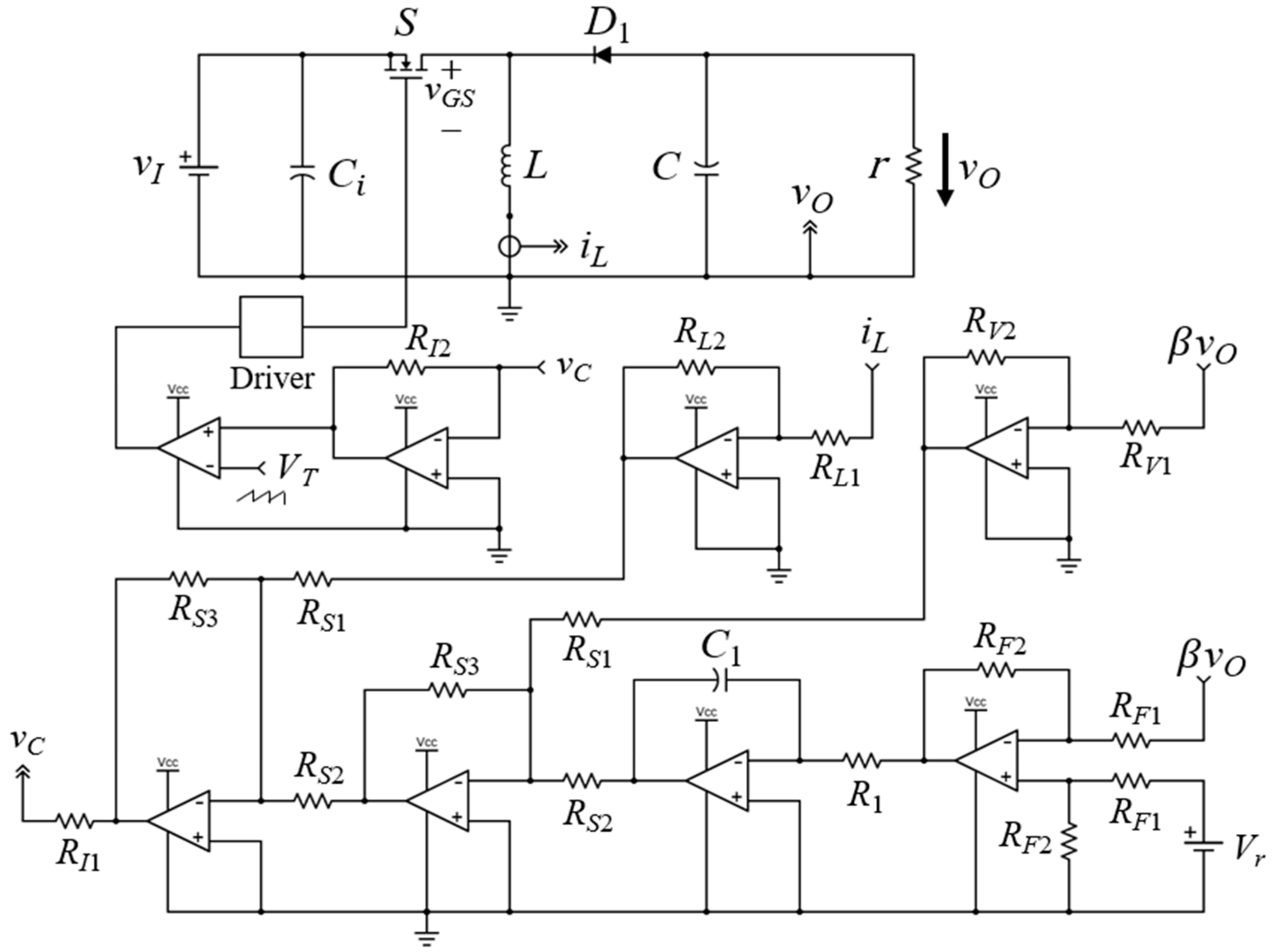
4. Realization of Analog Control Circuit

The control scheme given in Figure 4 should be converted to an analog control circuit that can easily be built using electronic components. The schematic of the proposed control circuit is given in Figure 5. The control circuit is made up of op-amps, resistors, and a capacitor. Despite the nonidealities and tolerances of the electronic elements, the overall control circuit must reflect the mathematical expression of the given control law, which is designed via the pole placement technique.
The design steps of the state feedback with an integral control circuit are summarized as follows:
  • Voltage sensor gain β : The buck-boost converter is designed to convert 28 V to 12 V. If the reference voltage V r = 2 V, then the feedback network gain β is V r V o = 2 12 = 1 6 ;
  • Summing, inverting, and differential op-amps: The gain of the summing, inverting, and differential op-maps in the control circuit is unity. Thus, the resistors of the summing op-amps R S 1 , R S 2 , and R S 3 , inverting op-amp R I 1 and R I 2 , and differential op-amp R F 1 and R F 2 are set to 5.1 kΩ;
  • Pulse-Width Modulator: The peak ramp voltage V T is set to 2 V, whereas the switching frequency f s is 100 kHz.
  • Inductor current gain K 1 : In the control design section, the gain of the inductor current K 1 has been computed as 0.011. Since the gain K 1 = R L 2 R L 1 , the resistor R L 1 and R L 2 can be set to 100 kΩ and 1.1 kΩ, respectively;
  • Output voltage gain K 2 : In the control design section, the gain of the output voltage K 2 has been computed as 0.17. Since the gain K 2 = R V 2 R V 1 , the resistor R V 2 and R V 1 can be set to 100 kΩ and 17 kΩ, respectively;
  • Integral gain K 3 : As reported in [26], the integral gain is defined as K 3 = 1 R 1 C 1 . In the control design section, the gain K 3 has been computed as 600. If the resistor R 1 is assumed to be 33 kΩ, then the capacitor C 1 is 56 nF;
It should be noted that accurate output voltage and inductor current sensors are required to measure the control state variables. The inductor current measurement is important in the state feedback with an integral control system to improve the transient response characteristics and handle the non-minimum phase power converter [27]. General-purpose op-amps such as LF357 can be utilized to build the state feedback with the integral control circuit.
Additionally, the design procedure of the control circuit given above does not include the selection of the pulse-width modulator and the high-side gate driver of the MOSFET. The mitigations for over-voltage protection, over-current protection, EMC/EMI compatibility, and other practical engineering aspects should also be considered to develop an experimental prototype for testing and evaluation.

5. Flowchart of State-Feedback with Integral Control Design

The step-by-step design procedure of the state-feedback with integral control of the dc-dc buck-boost converter is summarized in a flowchart as shown in Figure 6.
First, the linearized small-signal averaged model of the power converter is derived in state-space form as defined in (5) and (6). The next step is to construct the closed-loop power converter dynamics as shown in (15), from which the matrices A , B , and C are obtained. Subsequently, the rank of the controllability matrix is computed to confirm that the pair [ A ,   B ] is controllable.
The dominant closed-loop poles are obtained using the characteristic equation of the second-order system given in (21). Next, based on (22), the desired percentage overshoot and settling time yield the required damping ratio and natural frequency, which give the desired dominant poles. Since the augmented model contains three state variables, the third pole should be placed far to the left on the s-plane in order to maintain the desired transient response. Then, the desired closed-loop poles are lumped together as shown in (23), and the state-feedback control gains given in (24) are computed using the acker command in MATLAB.
Finally, the SIMULINK model of the state-feedback with an integral-controlled PWM dc-dc buck-boost converter is simulated to verify the tracking performance of the control system. If the desired response is achieved, the control equation is converted to an electronic circuit as explained in Section 4. However, if the system response requires further enhancement, the closed-loop poles’ location can be adjusted and the controller gains are re-calculated for verification.

6. Results and Discussion

6.1. Validation of Control Design Approach

The schematic of state-feedback with an integral control circuit in Figure 5 has been constructed using Simscape Electrical in MATLAB. In order to validate the control design methodology, the electronic control circuit has been compared with the MATLAB/SIMULINK nonlinear model of the closed-loop control system given in Figure 4. The power converter parameters are defined in Table 2. The proposed state feedback controller gains are given in (24), whereas the corresponding electronic control circuit elements are defined in Section 4.
The MATLAB/SIMULINK model and the closed-loop power converter circuit in Simscape Electrical are simulated and compared under nominal operating conditions (load resistance R = 3 Ω and input voltage VI = 28 V). The simulation of the two closed-loop control schemes is conducted in MATLAB using (Automatic) solver and 0.1 µs step-size. The waveforms of the ramp voltage VT, control voltage u, gate-to-source voltage vGS, the inductor current iL, and output voltage vO during steady-state are shown in Figure 7. The simulation results of the mathematical closed-loop power converter model in SIMULINK and the corresponding closed-loop power converter circuit in Simscape Electrical are depicted in Figure 7a and Figure 7b, respectively.
It can be seen that the waveforms obtained from the mathematical model in Figure 7a and those obtained from the corresponding electronic circuit in Figure 7b are identical. That means the mathematical model of the power converter mathematical model emulates the power converter circuit dynamics successfully. Additionally, the state feedback with integral control law has been represented by the analog control circuit properly, which validates the control circuit design approach.
Notably, the dc output voltage is regulated at −12 V with a duty cycle of 0.336, whereas the switching frequency of the ramp voltage waveform VT is 100 kHz. The negative output voltage is due to the topology of the inverting dc-dc buck-boost converter. It can also be seen that the power converter operates in CCM because the inductor current waveform is maintained above zero. The average value of the inductor current is around 5.99 A.

6.2. Rejection of Line and Load Variations

The performance of the state feedback with an integral control system has been investigated considering step change in input voltage vI and load current iO. The output voltage response during line variation is shown in Figure 8. In Figure 8a, as vI changes from 28 V to 33 V, the percentage overshoot PO and settling time ts are about 2.6% and 5.50 ms, respectively. Moreover, when the input voltage vI changes from 28 V to 23 V as shown in Figure 8b, the maximum PO and ts are around 3.5% and 5.5 ms, respectively. In both cases, it can be noticed that vO is regulated at the desired value while maintaining consistent dynamics during the line variations.
On the other hand, the output voltage responses to a step change in load current iO are depicted in Figure 9. As shown in Figure 9a, when the load current iO increases from 4 A to 6 A, the output voltage vO exhibits a maximum percentage overshoot PO of 2% with settling time ts of 4 ms. However, when the load current iO decreases from 4 A to 2.5 A, Figure 9b shows that the output voltage vO has a maximum percentage undershoot PO of 1% and reaches the steady-state value after 3.5 ms.
The simulation results show the disturbance rejection capability of the proposed control system. Although the control design is conducted based on the linearized ideal state-space model, the control circuit can still handle the nonlinear dynamics of the dc-dc buck-boost converter. In addition, the percentage overshoot and settling time of the output voltage response remain within the desired limits (maximum percentage overshoot PO ≤ 5% and settling time ts ≤ 5 ms).

6.3. Tracking of Time-Varying Reference Voltage

The output voltage response vO during step changes in the reference voltage Vr is shown in Figure 10. The power converter operates at nominal operating conditions (load resistance R = 3 Ω and input voltage VI = 28 V). It can be noticed that when the reference voltage Vr steps down from 2 V to 1.5 V, the output voltage vO follows the desired trajectory vd and shifts down from −12 V to −9 V. Likewise, when the reference voltage Vr steps up from 2 V to 2.5 V, then the output voltage vO tracks the desired trajectory vd and shifts down from −12 V to −15 V. In both cases, the output voltage vO takes about 5.5 ms with no percentage overshoot to reach the steady-state value. Thus, the simulation results show that the proposed control circuit tracks the desired trajectory effectively.
However, the output voltage response of the closed-loop nonlinear power converter circuit in Figure 10 exhibits a longer settling time as compared to that of the closed-loop ideal linearized power converter model shown in Figure 3. The discrepancy between the characteristics of the two responses is due to the inclusion of the nonlinearity and parasitic components of the dc-dc converter and the control circuit, which are not considered in the linearized closed-loop power converter model. Thus, the nonlinearities and modeling uncertainty of the power converter increase the settling time of the closed-loop system response.
Table 3 summarizes the characteristics of the state-feedback with an integral controlled dc-dc buck-boost converter under step changes in input voltage, load current, and the reference voltage. It can be noticed that the output voltage is maintained at −12 V during line and load variations. However, when the reference voltage changes, the output voltage follows the new desired trajectory as shown in Figure 10.

7. Conclusions

The state feedback with integral control circuit using the pole placement technique has been developed for the inverting PWM dc-dc buck-boost converter in CCM. The control design methodology and the realization of the proposed control circuit have been introduced. The SIMULINK model and the corresponding Simscape Electrical circuit of the closed-loop power converter have been simulated in MATLAB to validate the design approach. It has been observed that the simulation results of the nonlinear closed-loop power converter model and the corresponding closed-loop power converter circuit are in good agreement. The pole placement technique results in a control law that places the closed-loop poles at the desired location on the left-half plane (LHP) and achieves the desired transient response. Furthermore, the state feedback with integral control eliminates the steady-state error at the output voltage and provides precise tracking performance. It has been shown that the line variation of 5 V and load variation of 2 A around the nominal operating point have been rejected with a percentage overshoot of 3.5% and settling time of 5.5 ms.
The state feedback with an integral control scheme is simple and implementable using op-amps and analog components, which is attractive for commercial and low-cost industrial applications. The proposed control design approach is flexible, which allows the designer to freely choose the closed-loop poles’ location, compute the controller gains that meet the requirements, and convert the control equation to an electronic control circuit. The controller gains of the control circuit can further be tuned to compensate for actual power converter dynamics and improve the transient response characteristics. On the contrary, if a digital signal processor is chosen to implement the state feedback control algorithm, then the control law must be discretized, and further analysis is required in the z-domain to maintain the stability of the digital control system. Hence, the proposed design technique introduces a competitive alternative for embedded system-based control implementation.

Author Contributions

Conceptualization, H.A.-B.; methodology, H.A.-B.; software, H.A.-B.; validation, M.K.K.; formal analysis, H.A.-B.; resources, M.K.K.; writing—original draft preparation, A.S.; writing—review and editing, M.K.K. visualization, A.S.; All authors have read and agreed to the published version of the manuscript.

Funding

This research received no external funding.

Institutional Review Board Statement

Not applicable.

Informed Consent Statement

Not applicable.

Data Availability Statement

Not applicable.

Conflicts of Interest

The authors declare no conflict of interest.

Abbreviations

List of Acronyms
PWMpulse-width modulated
EVelectric vehicle
NIOCneural inverse optimal control
EKFextended Kalman filter
MPCmodel predictive control
LHPleft-half-plane
CPLconstant power load
HILhardware-in-the-loop
CCMcontinuous conduction mode
MOSFETmetal-oxide-semiconductor field-effect transistor
ESRequivalent series resistance
POpercentage overshoot
CP characteristic polynomial
EMCelectromagnetic compatibility
EMIelectromagnetic interference
List of Symbols
SMOSFET
D1Diode
LInductor
COutput capacitor
r L Inductor ESR
r C Capacitor ESR
r F Diode forward resistance
V F Diode threshold voltage
r DS MOSFET on-resistance
v I Large-signal input voltage
v O Large-signal output voltage
rLarge-signal load resistance
i O Large-signal load current
d T Large-signal time interval when S is ON
d T Large-signal time interval when S is OFF
i L Large-signal inductor current
v C Large-signal capacitor voltage
V I Steady-state input voltage
V O Steady-state output voltage
R Steady-state load resistance
I L Steady-state inductor current
D T Steady-state time interval when S is ON
D T Steady-state time interval when S is OFF
i ~ L Small-signal ac inductor current
v ~ C Small-signal ac capacitor voltage
d ~ Small-signal ac duty cycle
x State variables vector
A State matrix
B Input matrix
C Output matrix
D Direct transmission matrix
Co Controllability matrix
uSystem input
ySystem output
V r Desired reference voltage
K Constant gains vector
Θ Zeros vector
tsSettling time
ζ Damping ratio
ω n Natural frequency
P Desired closed-loop poles vector
β Voltage sensor gain
V T Peak ramp voltage
f s Switching frequency
K 1 Inductor current gain
K 2 Output voltage gain
K 3 Integral gain

References

  1. Ruz-Hernandez, J.A.; Djilali, L.; Canul, M.A.R.; Boukhnifer, M.; Sanchez, E.N. Neural Inverse Optimal Control of a Regenerative Braking System for Electric Vehicles. Energies 2022, 15, 8975. [Google Scholar] [CrossRef]
  2. Sankar, R.S.R.; Deepika, K.K.; Alsharef, M.; Alamri, B. A Smart ANN-Based Converter for Efficient Bidirectional Power Flow in Hybrid Electric Vehicles. Electronics 2022, 11, 3564. [Google Scholar] [CrossRef]
  3. Danyali, S.; Aghaei, O.; Shirkhani, M.; Aazami, R.; Tavoosi, J.; Mohammadzadeh, A.; Mosavi, A. A New Model Predictive Control Method for Buck-Boost Inverter-Based Photovoltaic Systems. Sustainability 2022, 14, 11731. [Google Scholar] [CrossRef]
  4. Murillo-Yarce, D.; Riffo, S.; Restrepo, C.; González-Castaño, C.; Garcés, A. Model Predictive Control for Stabilization of DC Microgrids in Island Mode Operation. Mathematics 2022, 10, 3384. [Google Scholar] [CrossRef]
  5. Kahani, R.; Jamil, M.; Iqbal, M.T. Direct Model Reference Adaptive Control of a Boost Converter for Voltage Regulation in Microgrids. Energies 2022, 15, 5080. [Google Scholar] [CrossRef]
  6. Jiang, Y.; Jin, X.; Wang, H.; Fu, Y.; Ge, W.; Yang, B.; Yu, T. Optimal Nonlinear Adaptive Control for Voltage Source Converters via Memetic Salp Swarm Algorithm: Design and Hardware Implementation. Processes 2019, 7, 490. [Google Scholar] [CrossRef]
  7. Hamed, S.B.; Hamed, M.B.; Sbita, L.; Bajaj, M.; Blazek, V.; Prokop, L.; Misak, S.; Ghoneim, S.S.M. Robust Optimization and Power Management of a Triple Junction Photovoltaic Electric Vehicle with Battery Storage. Sensors 2022, 22, 6123. [Google Scholar] [CrossRef]
  8. Lu, Y.; Zhu, H.; Huang, X.; Lorenz, R.D. Inverse-System Decoupling Control of DC/DC Converters. Energies 2019, 12, 179. [Google Scholar] [CrossRef]
  9. Solsona, J.A.; Jorge, S.G.; Busada, C.A. Modeling and Nonlinear Control of dc–dc Converters for Microgrid Applications. Sustainability 2022, 14, 16889. [Google Scholar] [CrossRef]
  10. Broday, G.R.; Lopes, L.A.C.; Damm, G. Exact Feedback Linearization of a Multi-Variable Controller for a Bi-Directional DC-DC Converter as Interface of an Energy Storage System. Energies 2022, 15, 7923. [Google Scholar] [CrossRef]
  11. Broday, G.R.; Damm, G.; Pasillas-Lépine, W.; Lopes, L.A.C. A Unified Controller for Multi-State Operation of the Bi-Directional Buck–Boost DC-DC Converter. Energies 2021, 14, 7921. [Google Scholar] [CrossRef]
  12. Csizmadia, M.; Kuczmann, M.; Orosz, T. A Novel Control Scheme Based on Exact Feedback Linearization Achieving Robust Constant Voltage for Boost Converter. Electronics 2023, 12, 57. [Google Scholar] [CrossRef]
  13. Chen, P.; Liu, J.; Xiao, F.; Zhu, Z.; Huang, Z. Lyapunov-Function-Based Feedback Linearization Control Strategy of Modular Multilevel Converter–Bidirectional DC–DC Converter for Vessel Integrated Power Systems. Energies 2021, 14, 4691. [Google Scholar] [CrossRef]
  14. Sira-Ramirez, H.; Silva-Ortigoza, R. Control Design Techniques in Power Electronics Devices; Springer: London, UK, 2006. [Google Scholar]
  15. Bajoria, N.; Sahu, P.; Nema, R.K.; Nema, S. Overview of different control schemes used for controlling of DC-DC converters. In Proceedings of the 2016 International Conference on Electrical Power and Energy Systems (ICEPES), Bhopal, India, 14–16 December 2016; pp. 75–82. [Google Scholar]
  16. Gkizas, G.; Yfoulis, C.; Amanatidis, C.; Stergiopoulos, F.; Giaouris, D.; Ziogou, C.; Voutetakis, S.; Papadopoulou, S. Digital state-feedback control of an interleaved DC-DC boost converter with bifurcation analysis. Cont. Eng. Pract. 2018, 73, 100–111. [Google Scholar] [CrossRef]
  17. Pegueroles-Queralt, J.; Bianchi, F.D.; Gomis-Bellmunt, O. A Power Smoothing System Based on Supercapacitors for Renewable Distributed Generation. IEEE Trans. Ind. Electron. 2015, 62, 343–350. [Google Scholar] [CrossRef]
  18. Hajizadeh, A.; Shahirinia, A.H.; Namjoo, N.; Yu, D.C. Self-tuning indirect adaptive control of non-inverting buck-boost converter. IET Power Electron. 2015, 8, 2299–2306. [Google Scholar] [CrossRef]
  19. Czarkowski, D.; Kazimierczuk, M.K. Application of state feedback with integral control to pulse-width modulated push-pull DC-DC convertor. IEE Proc.-Control Theory Appl. 1994, 141, 99–103. [Google Scholar] [CrossRef]
  20. Abdurraqeeb, A.M.; Al-Shamma’a, A.A.; Alkuhayli, A.; Noman, A.M.; Addoweesh, K.E. RST Digital Robust Control for DC/DC Buck Converter Feeding Constant Power Load. Mathematics 2022, 10, 1782. [Google Scholar] [CrossRef]
  21. Koundi, M.; El Idrissi, Z.; El Fadil, H.; Belhaj, F.Z.; Lassioui, A.; Gaouzi, K.; Rachid, A.; Giri, F. State-Feedback Control of Interleaved Buck–Boost DC–DC Power Converter with Continuous Input Current for Fuel Cell Energy Sources: Theoretical Design and Experimental Validation. World Electr. Veh. J. 2022, 13, 124. [Google Scholar] [CrossRef]
  22. Al-Baidhani, H.; Salvatierra, T.; Ordonez, R.; Kazimierczuk, M.K. Simplified nonlinear voltage-mode control of PWM DC-DC buck converter. IEEE Trans. Energy Conv. 2021, 36, 431–440. [Google Scholar] [CrossRef]
  23. Al-Baidhani, H.; Kazimierczuk, M.K. Simplified Double-Integral Sliding-Mode Control of PWM DC-AC Converter with Constant Switching Frequency. Appl. Sci. 2022, 12, 10312. [Google Scholar] [CrossRef]
  24. Al-Baidhani, H.; Kazimierczuk, M.K.; Ordóñez, R. Nonlinear Modelling and Control of PWM DC-DC Buck-Boost Converter for CCM. In Proceedings of the IECON 2018—44th Annual Conference of the IEEE Industrial Electronics Society, Washington, DC, USA, 21–23 October 2018; pp. 1374–1379. [Google Scholar]
  25. Golnaraghi, F.; Kuo, B. Automatic Control Systems, 9th ed.; John Wiley & Sons: Hoboken, NJ, USA, 2010. [Google Scholar]
  26. Kazimierczuk, M.K. Pulse-Width Modulated DC-DC Power Converters, 2nd ed.; John Wiley & Sons: Chichester, UK, 2016. [Google Scholar]
  27. Al-Baidhani, H.; Kazimierczuk, M.K. Simplified Nonlinear Current-Mode Control of DC-DC Cuk Converter for Low-Cost Industrial Applications. Sensors 2023, 23, 1462. [Google Scholar] [CrossRef]
Figure 1. (a) The inverting dc-dc buck-boost converter circuit. (b) The equivalent circuit of the non-ideal buck-boost converter in CCM.
Mathematics 11 02139 g001
Figure 2. The block diagram of the state feedback with integral control system.
Mathematics 11 02139 g002
Figure 3. The unit step response of the compensated dc-dc buck-boost converter.
Mathematics 11 02139 g003
Figure 4. MATLAB/SIMULINK model of state feedback with integral control system of inverting dc-dc buck-boost converter.
Mathematics 11 02139 g004
Figure 5. Schematic of state-feedback with integral controlled PWM dc-dc buck-boost converter circuit.
Mathematics 11 02139 g005
Figure 6. Flowchart of state-feedback with integral control design of dc-dc buck-boost converter.
Mathematics 11 02139 g006
Figure 7. Steady-state waveforms of (a) MATLAB/SIMULINK model and (b) Simscape Electrical circuit of the state feedback with integral control of PWM dc-dc buck-boost converter in CCM. The figures show the control input u, ramp voltage VT, gate-to-source voltage vGS, inductor current iL, and output voltage vO.
Mathematics 11 02139 g007
Figure 8. The tracking performance of the state feedback with integral control of inverting dc-dc buck-boost converter under line disturbance. (a) The output voltage response vO when the input voltage vI changes from 28 V to 33 V during the time interval 20 ≤ t ≤ 32.5 ms. (b) The output voltage response vO when the input voltage vI changes from 28 V to 23 V during the time interval 20 ≤ t ≤ 32.5 ms.
Mathematics 11 02139 g008
Figure 9. The tracking performance of the state feedback with integral control of inverting dc-dc buck-boost converter under load disturbance. (a) The output voltage response vO when the load current iO changes from 4 A to 6 A during the time interval 20 ≤ t ≤ 32.5 ms. (b) The output voltage response vO when the load current iO changes from 4 A to 2.5 A during the time interval 20 ≤ t ≤ 32.5 ms.
Mathematics 11 02139 g009
Figure 10. The output voltage response vO of the state feedback with integral control of PWM dc-dc buck-boost converter in CCM during a time-varying reference voltage Vr. The upper sub-figure shows the step changes in reference voltage Vr. The lower sub-figure shows the tracking performance of the output voltage response vO with respect to the desired trajectory vd.
Mathematics 11 02139 g010
Table 1. Modern control techniques of dc-dc power converters.
Control TechniqueAdvantagesDisadvantagesReferences
Neural inverse optimal control (NIOC)
  • Robustness against large disturbances.
  • Estimating converter dynamics.
  • Complexity of practical control system design.
  • High-cost control system implementation.
[1]
Artificial neural network-based control[2]
Model predictive control (MPC)
  • Fast dynamical response.
  • Accurate tracking performance.
Practical implementation has not been discussed.[3]
Centralized MPC
  • Fast dynamical response.
  • Less computational efforts than traditional MPC.
High-cost control system implementation.[4]
Direct model reference adaptive controlRobustness against voltage and frequency variations.Complexity of control system implementation.[5]
Optimal adaptive controlEstimation of uncertainties and disturbancesHigh-cost control system implementation (dSPACE).[6]
Lyapunov-based nonlinear controlRobustness against load variations.Practical implementation has not been covered.[7]
Inverse-system decoupling controlDisturbance rejection capability.Design procedure of control circuit has not been provided.[8]
Feedback linearization controlMitigation of CPL and zero dynamics.Design procedure of control circuit has not been provided.[9,10,11,12,13]
State-feedback control via pole placementPlacement of closed-loop poles at desired locations.Steady-state error issue.
Design procedure of control circuit has not been provided.
[14,15,16,17,18]
State-feedback with integral controlState variables regulation and steady-state error elimination.Design procedure of control circuit has not been introduced.
High-cost control system implementation (dSPACE).
[19]
pole placement control with sensitivity functionMitigation of CPL and non-minimum phase issue.[20]
Table 2. Parameters of dc-dc buck-boost converter [24].
DescriptionParameterValue
InductorL30 μH
Output capacitorC2.2 mF
Load resistanceR(1.2–12) Ω
Inductor ESRrL0.050 Ω
Output capacitor ESRrC0.006 Ω
MOSFET on-resistancerDS0.110 Ω
Diode forward resistancerF0.020 Ω
Diode threshold voltageVF0.700 V
Input voltageVI28 ± 4 V
Output voltageVO12 V
Switching frequencyfs100 kHz
Table 3. Characteristics of proposed control circuit response during step changes in load current, input voltage, and reference voltage.
Disturbance Type (∆iO, ∆vI, ∆Vr) Overshoot/Undershoot (%)Settling Time (ms)Output Voltage (V)
i O 4 A to 6.0 A 24−12
i O 4 A to 2.5 A 13.5−12
v I 28 V to 33 V 2.65.5−12
v I 28 V to 23 V 3.55.5−12
V r 2 V to 2.5 V 05.5−15
V r 2 V to 1.5 V 05.5−9
Disclaimer/Publisher’s Note: The statements, opinions and data contained in all publications are solely those of the individual author(s) and contributor(s) and not of MDPI and/or the editor(s). MDPI and/or the editor(s) disclaim responsibility for any injury to people or property resulting from any ideas, methods, instructions or products referred to in the content.

