
Sol–Gel Waveguide-Based Sensor for Structural Health Monitoring on Large Surfaces in Aerospace Domain

 , , , ,
  ,
,
Abstract
:1. Introduction
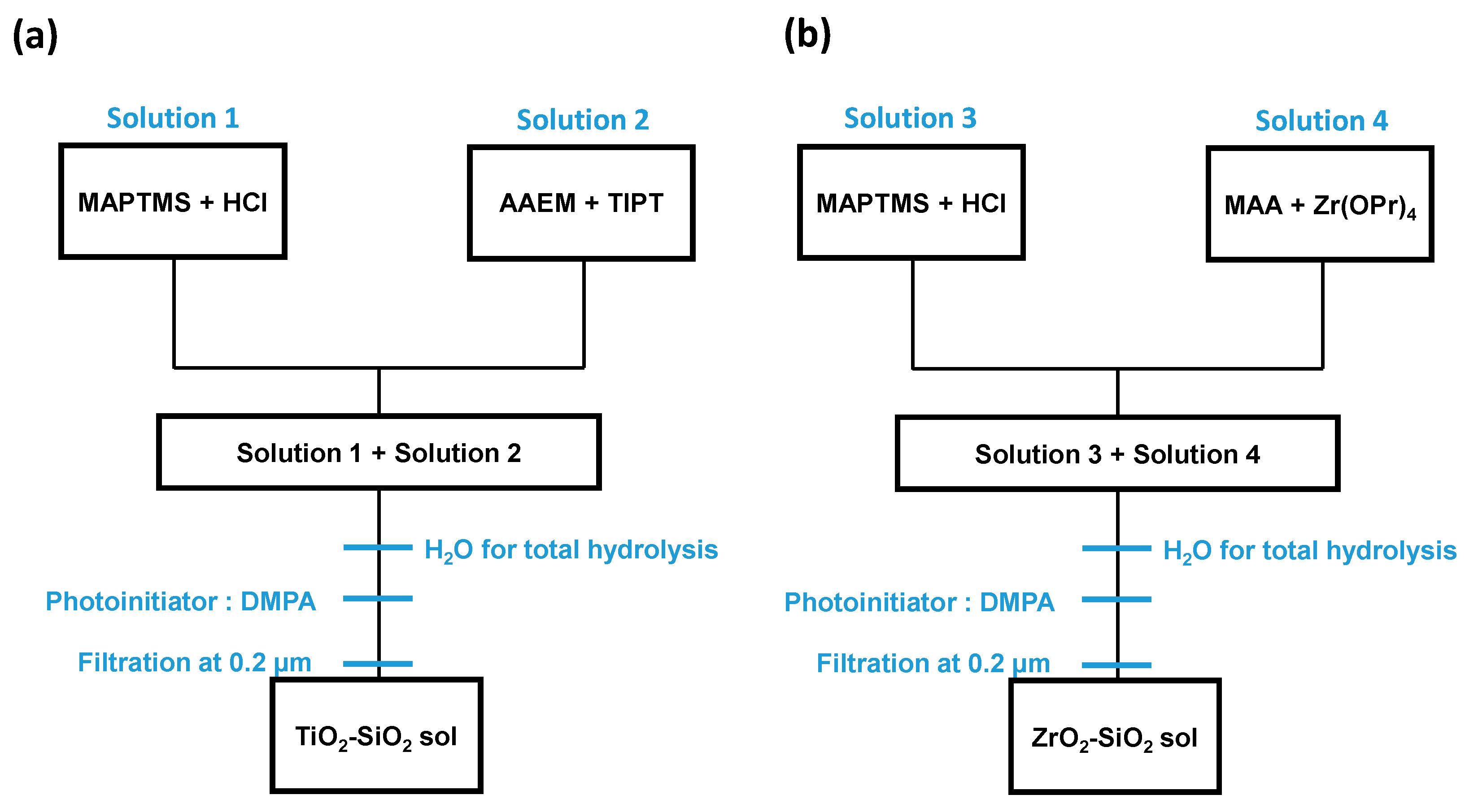
2. Materials and Methods
3. Results and Discussion
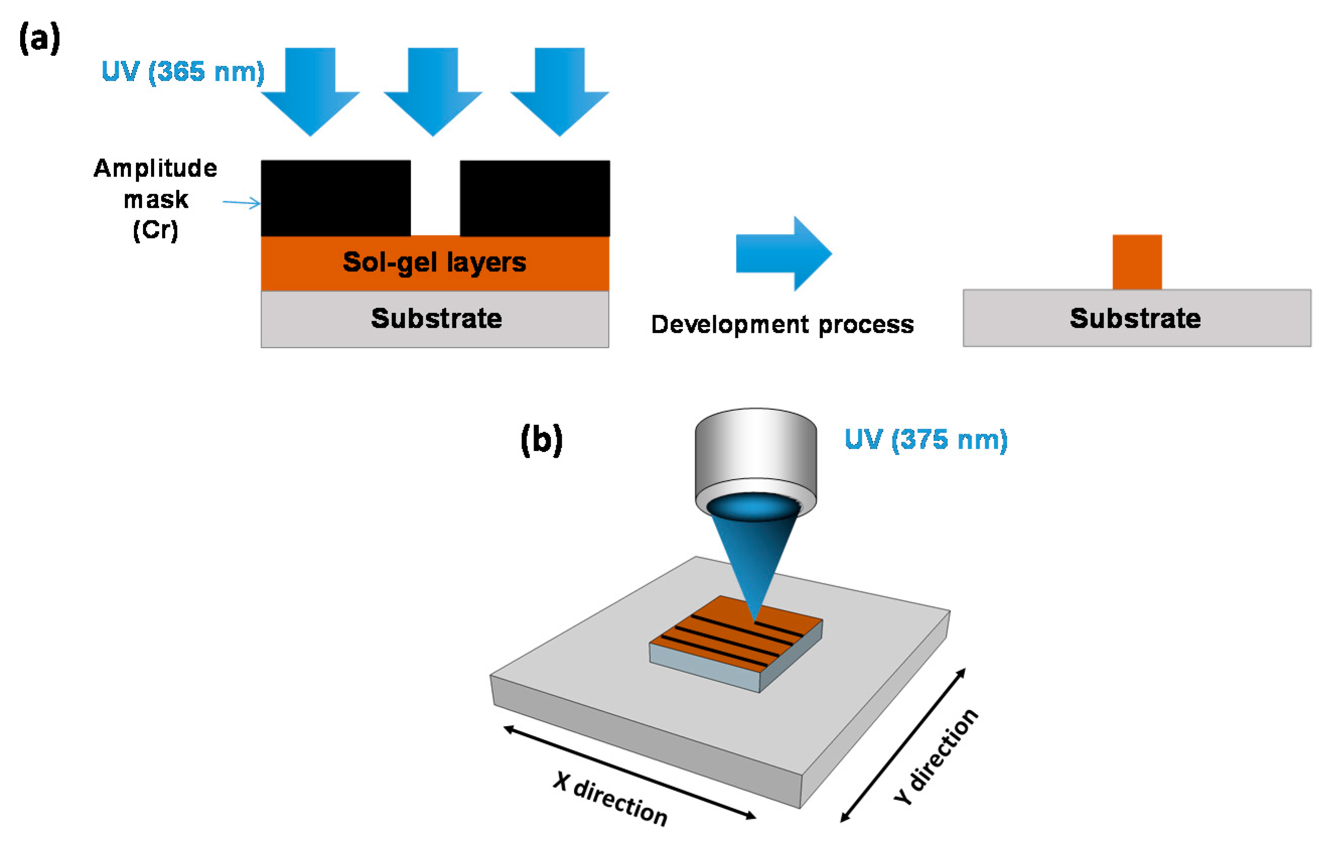
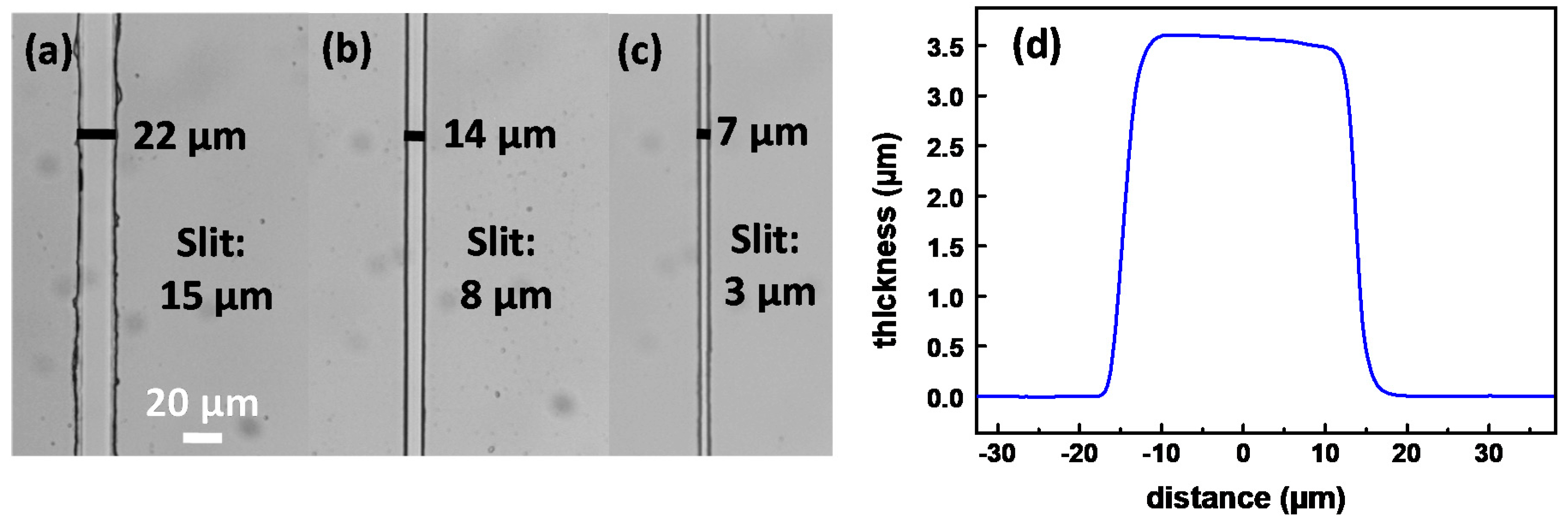
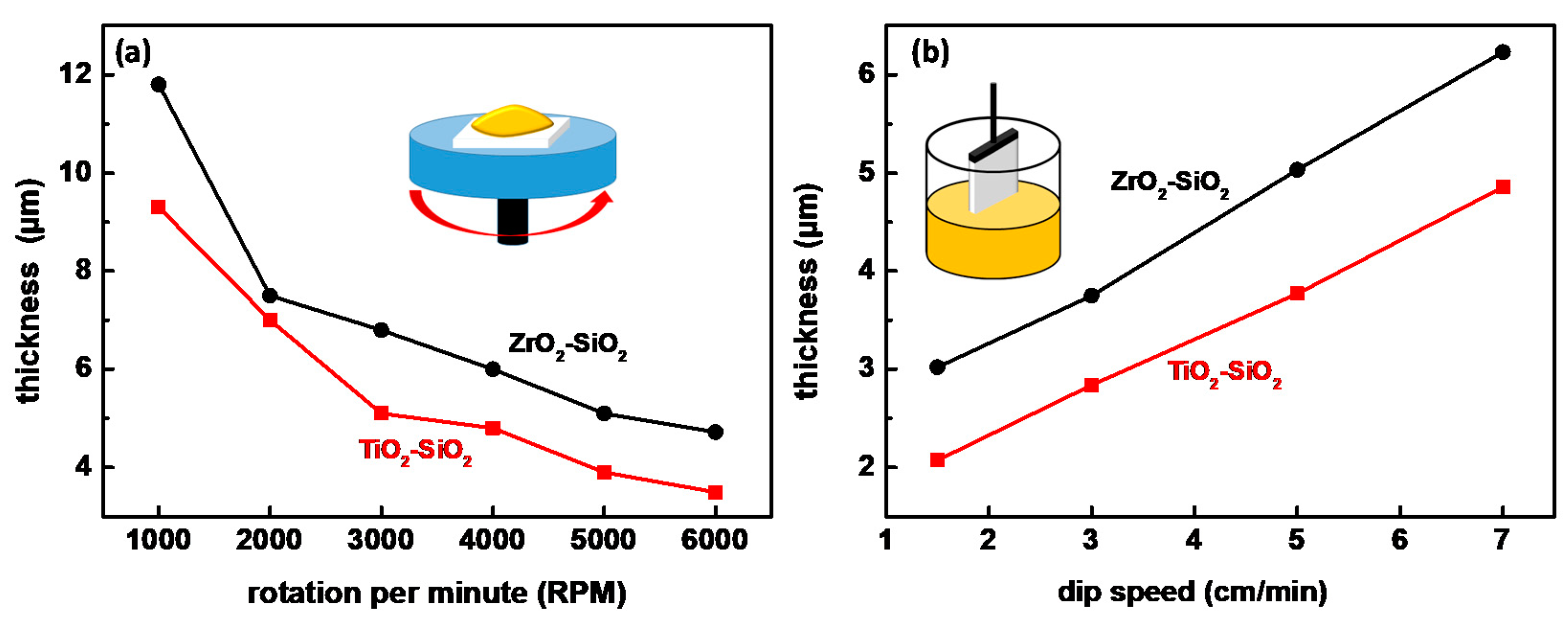
3.1. Amplitude Mask Method and Thicknesses Characterization
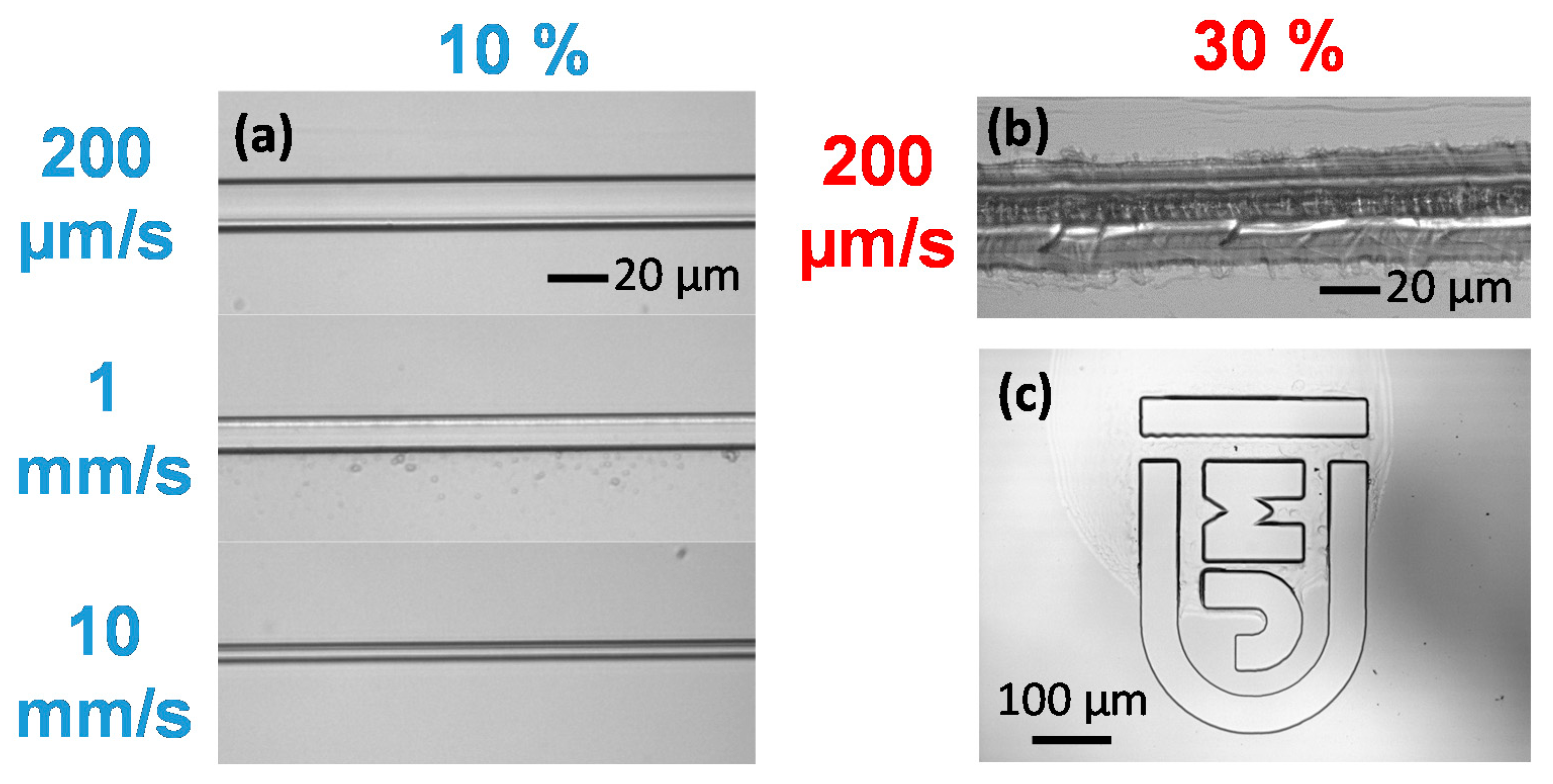
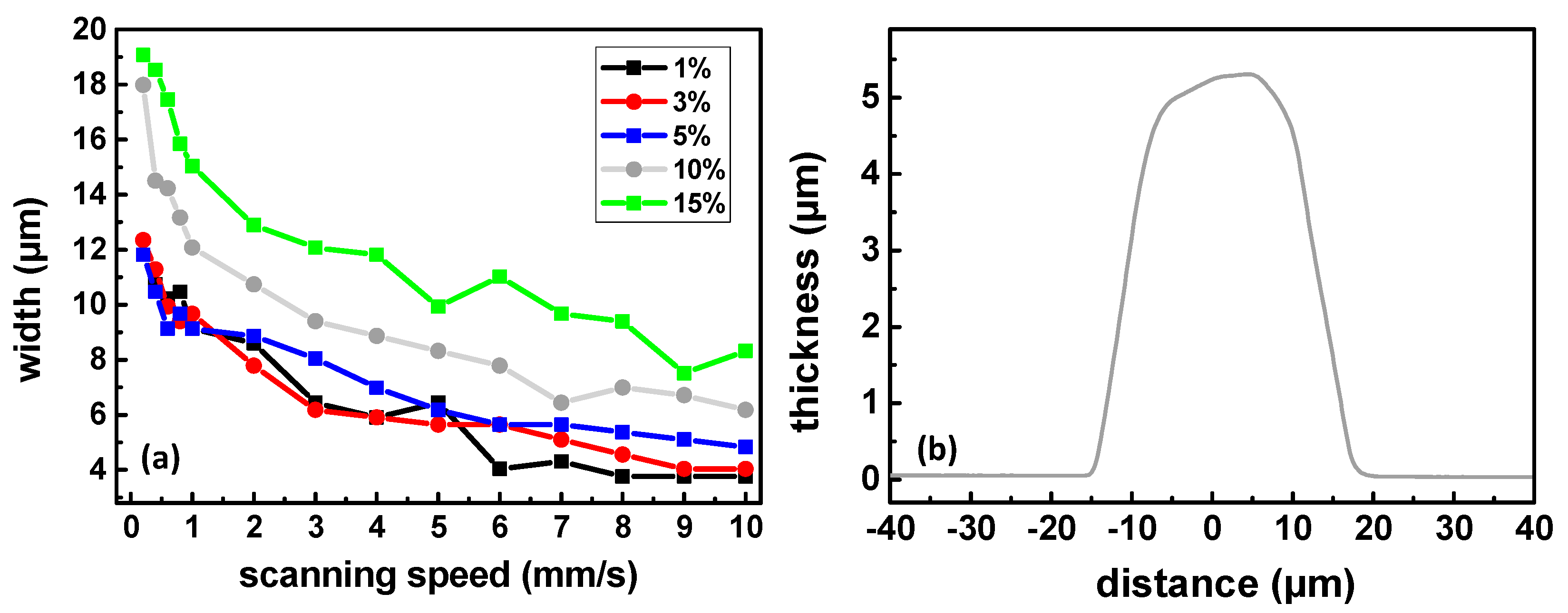
3.2. Direct Writing Technique
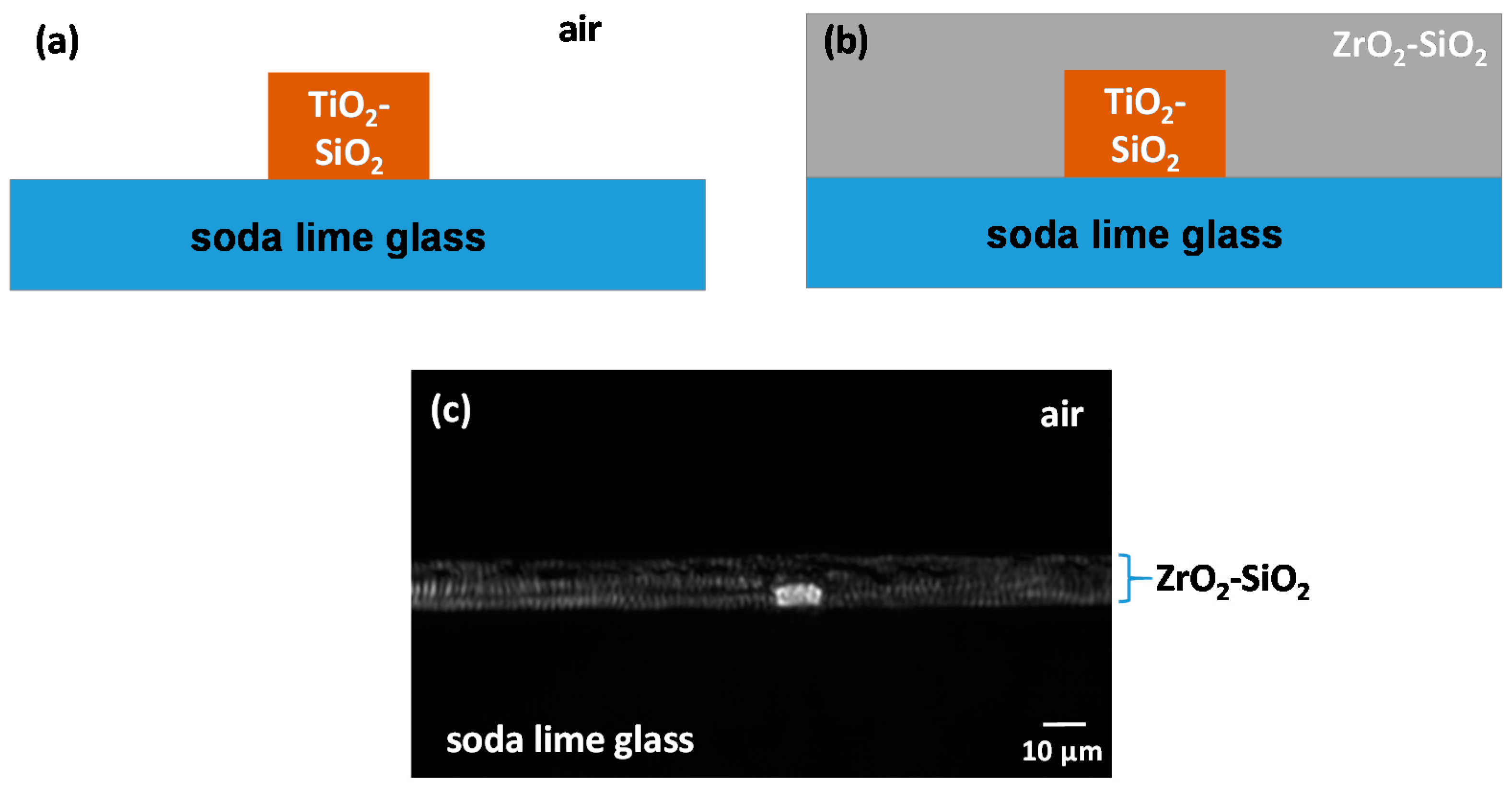
3.3. Creation of the Full Device: TiO2–SiO2 Core and ZrO2–SiO2 Cladding
3.4. Refractive Index Measurements
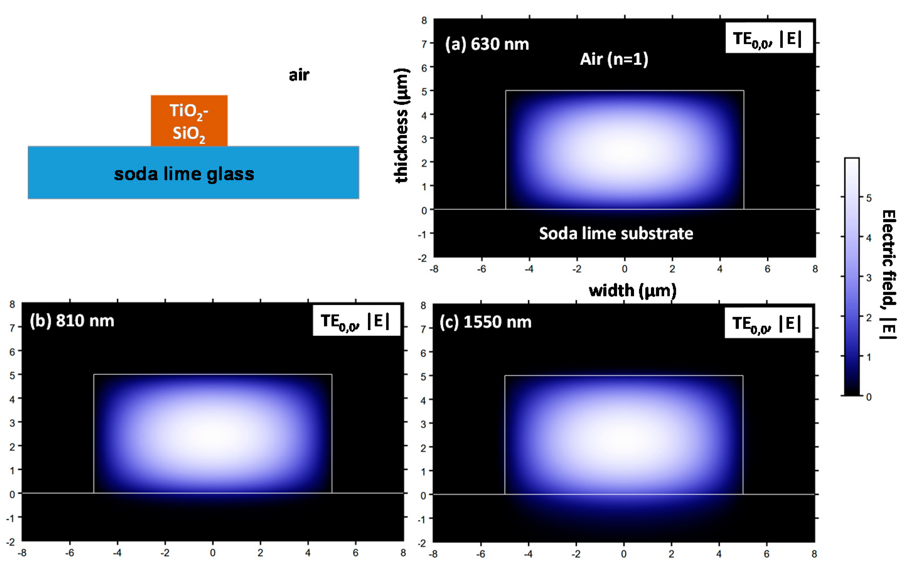
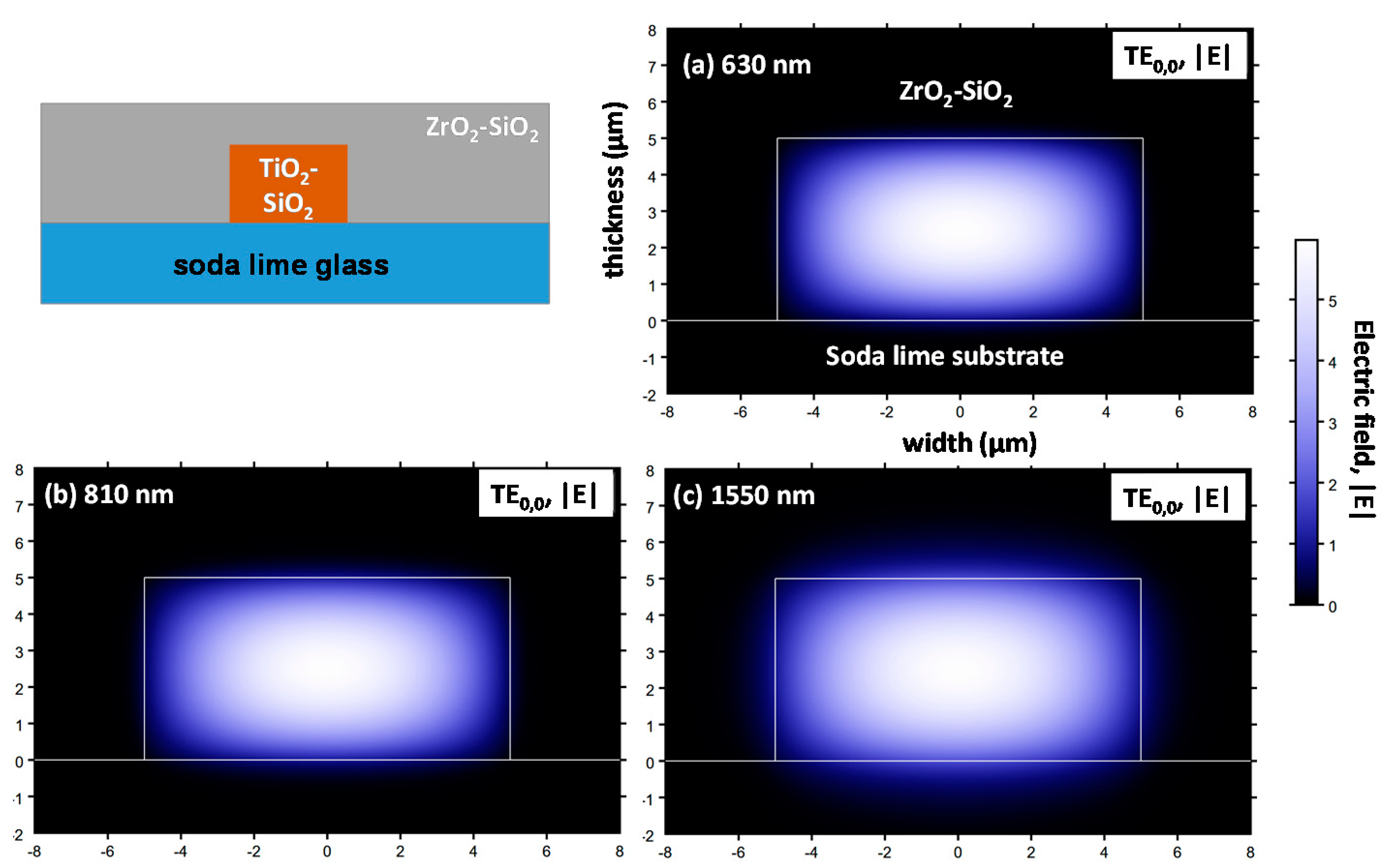
3.5. Simulation of the Mode Confinement: Transverse Electric (TE) Mode
3.6. Optical Properties of the Sol–Gel Device
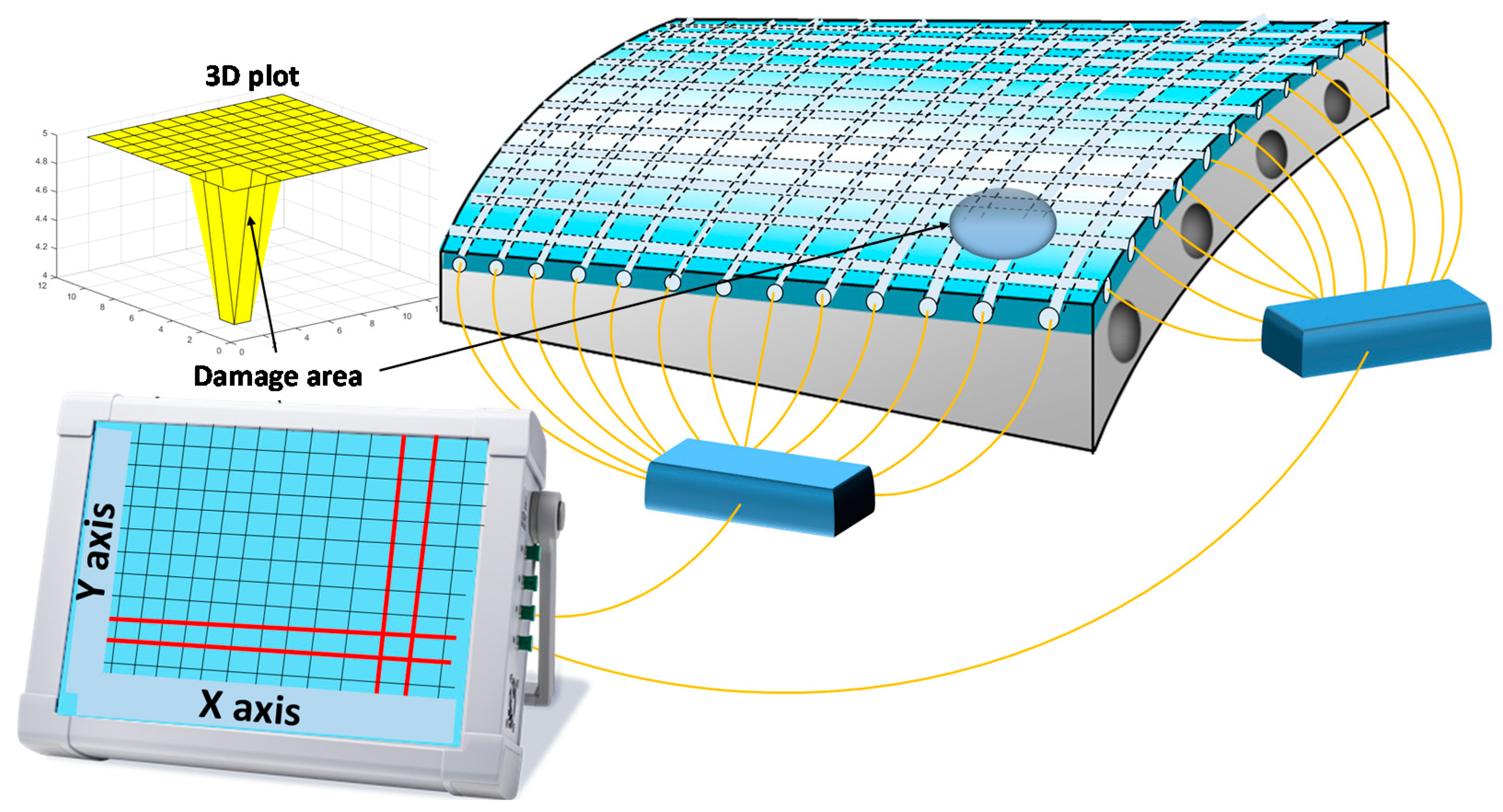
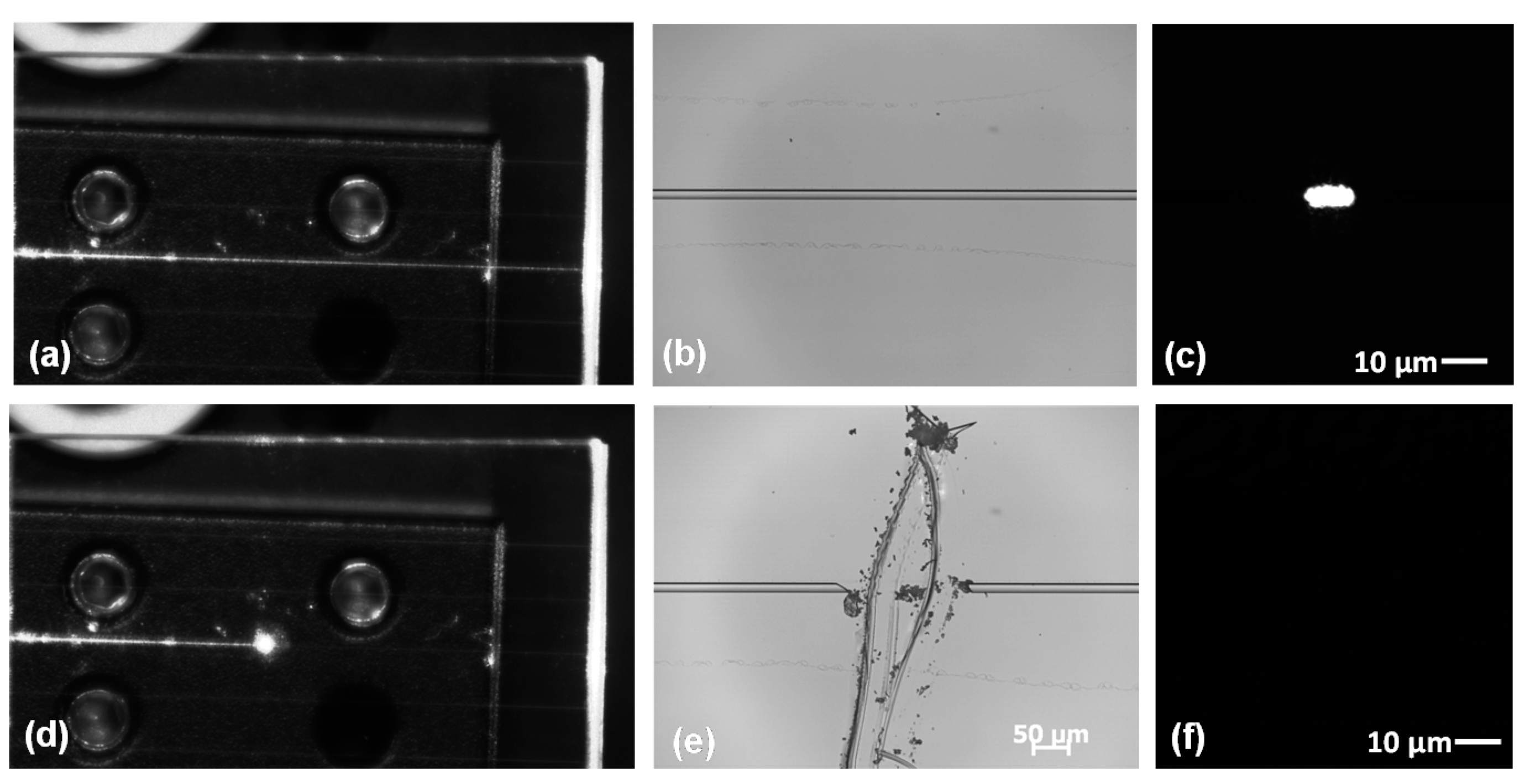
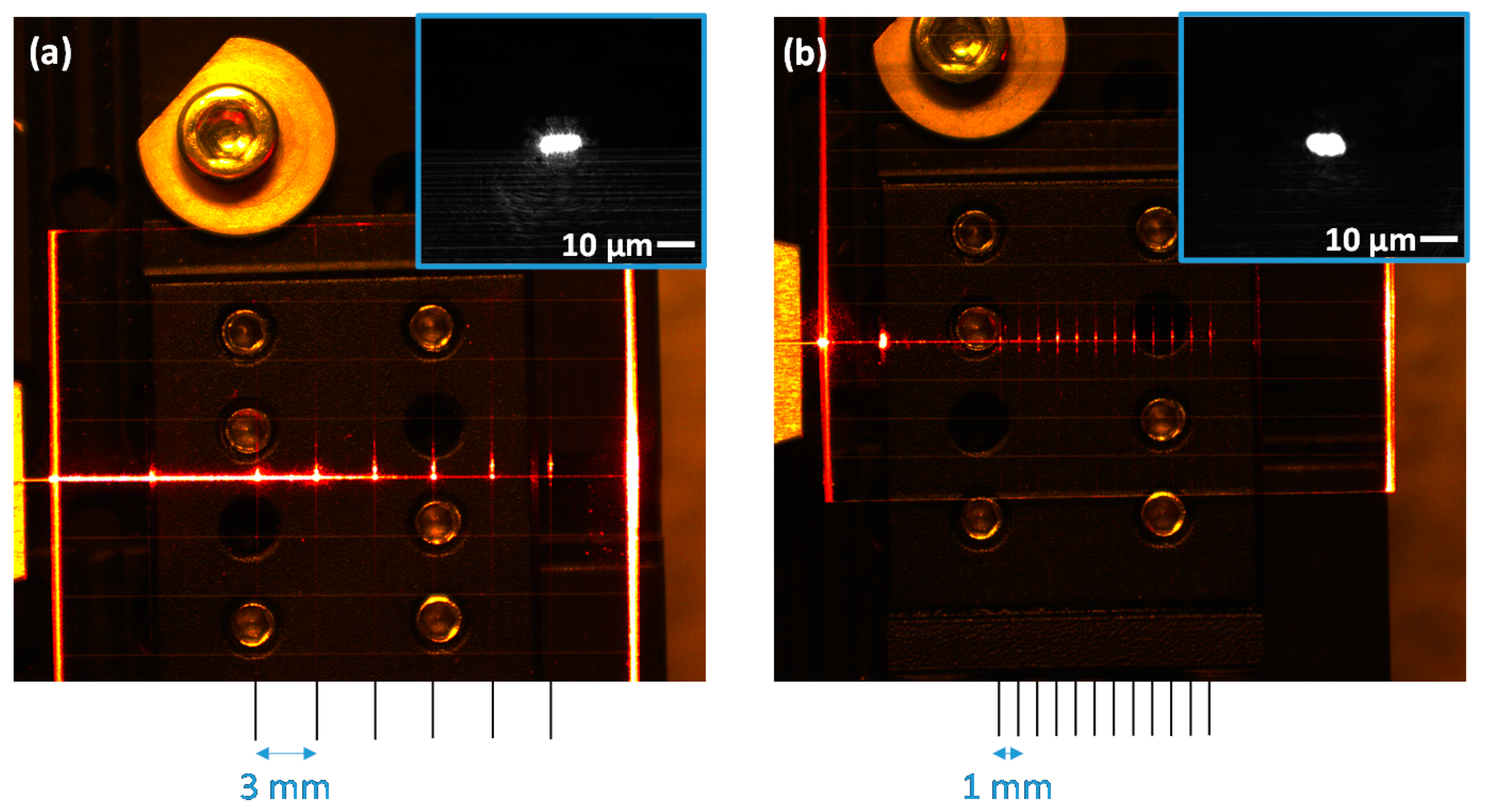
3.7. Damage Detection and TiO2–SiO2 Waveguide Matrix Characterization
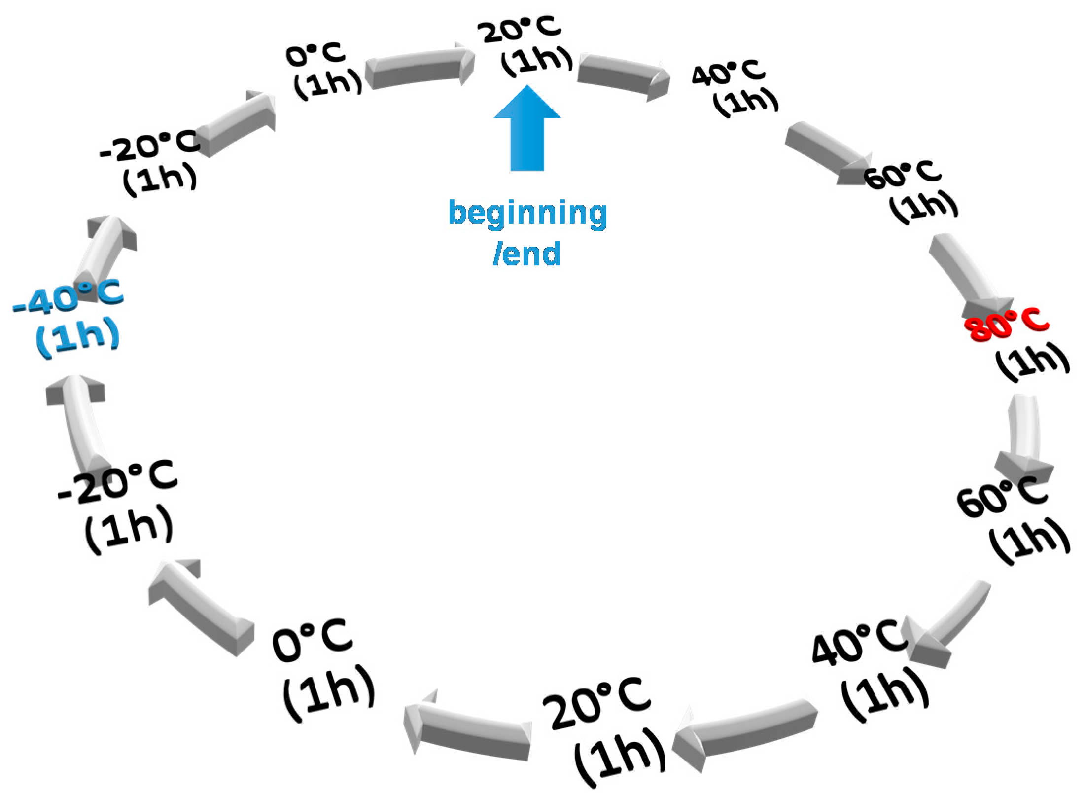
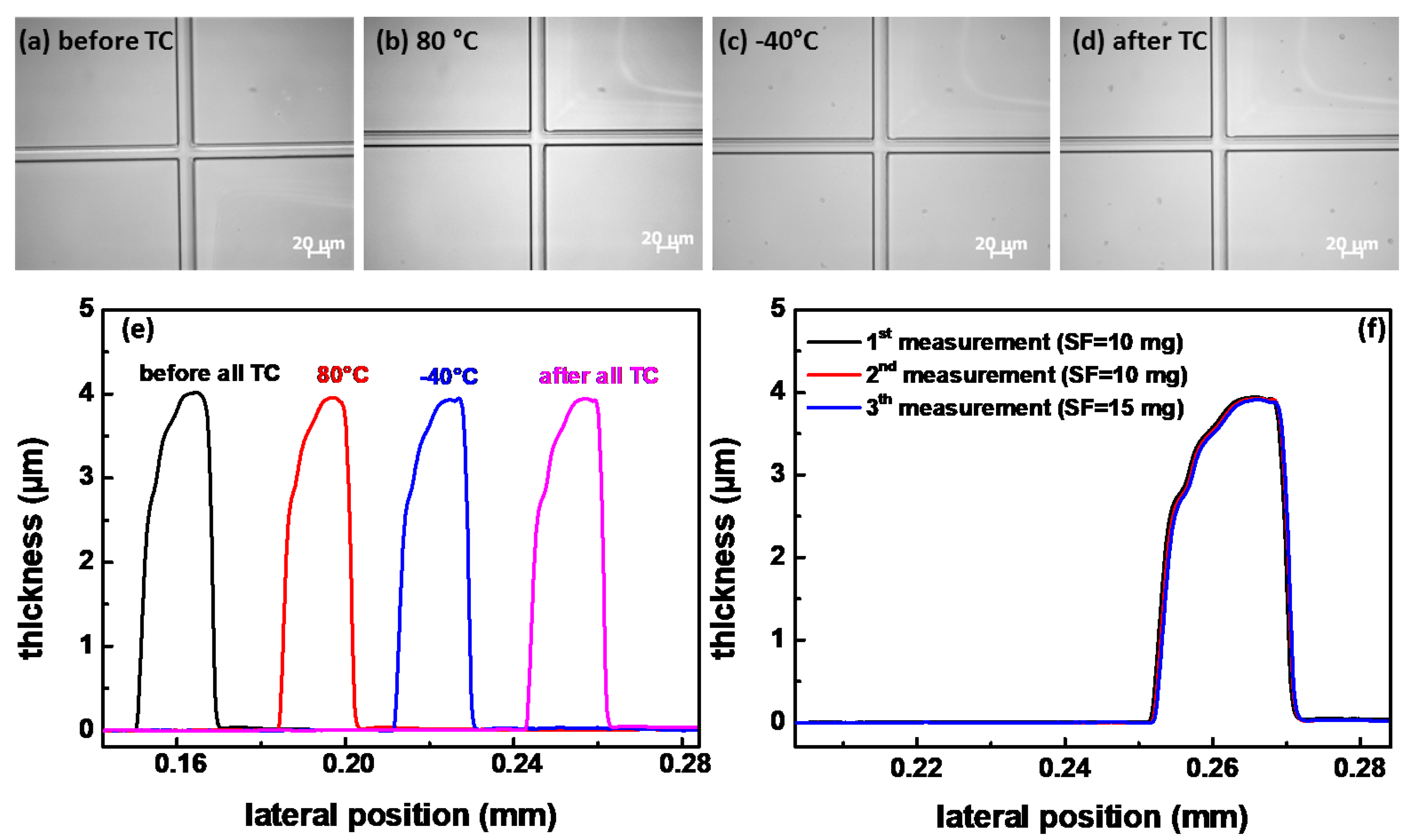
3.8. Thermal Behavior of TiO2–SiO2 Waveguides
4. Conclusions
Author Contributions
Funding
Institutional Review Board Statement
Informed Consent Statement
Acknowledgments
Conflicts of Interest
References
- Qing, X.; Li, W.; Wang, Y.; Sun, H. Piezoelectric Transducer-Based Structural Health Monitoring for Aircraft Applications. Sensors 2019, 19, 545. [Google Scholar] [CrossRef] [PubMed]
- Staszewski, W.J.; Mahzan, S.; Traynor, R. Health monitoring of aerospace composite structures—Active and passive approach. Compos. Sci. Technol. 2008, 69, 1678–1685. [Google Scholar] [CrossRef]
- Solimine, J.; Niezrecki, C.; Inalpolat, M. An experimental investigation into passive acoustic damage detection for structural health monitoring of wind turbine blades. Struct. Health Monit. 2020, 19, 1711–1725. [Google Scholar] [CrossRef]
- Di Sante, R. Fibre Optic Sensors for Structural Health Monitoring of Aircraft Composite Structures: Recent Advances and Applications. Sensors 2015, 15, 18666–18713. [Google Scholar] [CrossRef]
- Lee, B.H.; Kim, Y.H.; Park, K.S.; Eom, J.B.; Kim, M.J.; Rho, B.S.; Choi, H.Y. Interferometric Fiber Optic Sensors. Sensors 2012, 12, 2467–2486. [Google Scholar] [CrossRef] [Green Version]
- Takeda, N.; Okabe, Y.; Mizutani, T. Damage detection in composites using optical fibre sensors. Proc. Inst. Mech. Eng. G 2007, 221, 497–508. [Google Scholar] [CrossRef]
- Güemes, A.; Fernandez-Lopez, A.; Soller, B. Optical fiber distributed sensing- Physical principles and applications. Struct. Health Monit. 2010, 9, 233–245. [Google Scholar] [CrossRef]
- Agustín-Sáenz, C.; Santa Coloma, P.; Fernández-Carretero, F.J.; Brusciotti, F.; Brizuela, M. Design of Corrosion Protective and Antistatic Hybrid Sol–Gel Coatings on 6XXX AlMgSi Alloys for Aerospace Application. Coatings 2020, 10, 441. [Google Scholar] [CrossRef]
- Catauro, M.; Mozzati, M.C.; Bollino, F. Sol–gel hybrid materials for aerospace applications: Chemical characterization and comparative investigation of the magnetic properties. Acta Astronaut. 2015, 117, 153. [Google Scholar] [CrossRef]
- Ouahabi, A.; Thomas, M.; Kobayashi, M.; Jen, C.K. Structural health monitoring of aerospace structures with sol–gel spray sensors. Key Eng. Mater. 2007, 347, 505–510. [Google Scholar] [CrossRef] [Green Version]
- Hench, L.L.; West, J.K. The sol–gel process. Chem. Rev. 1990, 90, 33–72. [Google Scholar] [CrossRef]
- Kaczmarek, H.; Galka, P.P. Effect of irgacure 651 initiator on poly(methyl methacryltate) photostability studied by UV-Vis spectroscopy. Open Process Chem. J. 2008, 1, 8–11. [Google Scholar] [CrossRef]
- Segurola, J.; Allen, N.S.; Edge, M.; Roberts, I. Photochemistry and photoinduced chemical crosslinking activity of acrylated prepolymers by several commercial type I far UV photoinitiators. Polym. Degrad. Stab. 1999, 65, 153–160. [Google Scholar] [CrossRef]
- Jerónimo, P.C.A.; Araújo, A.N.; Montenegro, M.C.B.S.M. Optical sensors and biosensors based on sol–gel films. Talanta 2007, 72, 13–27. [Google Scholar] [CrossRef] [PubMed]
- Gelover, S.; Mondragón, P.; Jiménez, A. Titanium dioxide sol–gel deposited over glass and its application as a photocatalyst for water decontamination. J. Photochem. Photobiol. A 2003, 165, 241–246. [Google Scholar] [CrossRef]
- Oubaha, M.; Kribich, R.K.; Copperwhite, R.; Etienne, P.; O’Dwyer, K.; MacCraith, B.D.; Moreau, Y. New inorganic sol–gel material with high transparency at 1.55 µm. Opt. Commun. 2005, 253, 346–351. [Google Scholar] [CrossRef]
- Versace, D.; Oubaha, M.; Copperwhite, R.; Croutxé-Barghorn, C.; MacCraith, B. Waveguide fabrication in UV-photocurable sol–gel materials: Influence of the photoinitiating system. Thin Solid Film 2008, 516, 6448–6457. [Google Scholar] [CrossRef] [Green Version]
- Custom Photolithography System: Dilase 750. Available online: https://www.kloe-france.com/en/laser-lithography/photolithography-systems/direct-laser-writing/dilase-750 (accessed on 9 March 2021).
- Durgapal, P.; Ehrstein, J.R.; Nguyen, N.V. Thin film ellipsometry metrology. AIP Conf. Proc. 1998, 449, 121–131. [Google Scholar]
- Coudray, P.; Etienne, P.; Moreau, Y.; Porque, J.; Najafi, S. Sol–gel channel waveguide on silicon: Fast direct imprinting and low cost fabrication. Opt. Commun. 1997, 143, 199–202. [Google Scholar] [CrossRef]
- Coudray, P.; Etienne, P.; Moreau, Y. Integrated optics based on organo-mineral materials. Mat. Sci. Semincon. Process. 2000, 3, 331–337. [Google Scholar] [CrossRef]
- Pani, S.K.; Quiling, Y.; Wong, C.C.; Low, D.K.Y.; Zhang, X.; Lyer, M.K. Fabrication of buried hybrid sol–gel optical waveguides by femtosecond laser direct writing. Thin Solid Films 2006, 504, 336–340. [Google Scholar] [CrossRef]
- Li, A.; Wang, Z.; Liu, J.; Zeng, X. Low cost fabrication of SiO2 optical waveguides by laser direct writing on Ti-doped sol–gel films. Opt. Lasers Eng. 2011, 49, 351–355. [Google Scholar] [CrossRef]
- Franc, J.; Blanc, D.; Zerroukhi, A.; Chalamet, Y.; Last, A.; Destouches, N. Organo-silica–titania nanocomposite elaborated by sol–gel processing with tunable optical properties. Mater. Sci. Eng. B 2006, 129, 180–185. [Google Scholar] [CrossRef]
- Aspnes, D.E.; Studna, A.A. Dielectric functions and optical parameters of Si, Ge, GaP, GaAs, GaSb, InP, InAs, and InSb from 1.5 to 6.0 eV. Phys. Rev. B 1982, 27, 985–1009. [Google Scholar] [CrossRef]
- Chandler-Horowitz, D.; Amirtharaj, P.M. High-accuracy, midinfrared (450 cm−1 ≤ ω ≤ 4000 cm−1) refractive index values of silicon. J. Appl. Phys. 2005, 97, 123526–123534. [Google Scholar] [CrossRef]
- Royon, M.; Vocanson, F.; Jamon, D.; Marin, E.; Morana, A.; Boukenter, A.; Girard, S.; Ouerdane, Y.; Royer, F.; Jourlin, Y. Comparison between the UV and X-ray Photosensitivities of Hybrid TiO2-SiO2 Thin Layers. Materials 2020, 13, 3730. [Google Scholar] [CrossRef] [PubMed]
- Rubin, M. Optical properties of soda lime silica glass. Sol. Energy Mater. 1985, 12, 275–288. [Google Scholar] [CrossRef] [Green Version]
- Hammer, M. 2-D Multilayer Waveguide Mode Solver, Variational Effective Index Approximation. Available online: https://www.siio.eu/eims.html (accessed on 9 January 2021).
- Sakai, J.I.; Sasaki, J.; Kawai, K. Optical power confinement factor in a Bragg fiber: 2. Numerical results. J. Opt. Soc. Am. B 2007, 24, 20–27. [Google Scholar] [CrossRef]
- Li Vecchi, G.; Di Francesca, D.; Sabatier, C.; Girard, S.; Alessi, A.; Guttilla, A.; Robin, T.; Kadi, Y.; Brugger, M. Infrared radiation induced attenuation of radiation sensitive optical fibers: Influence of temperature and modal propagation. Opt. Fiber Technol. 2020, 55, 102166–102172. [Google Scholar] [CrossRef]


| Fluence (J/cm2) | Polymerization |
|---|---|
| 54 | No |
| 72 | Partial |
| 90 | Full |
| 108 | Full |
| 144 | Full |
| 180 | Full |
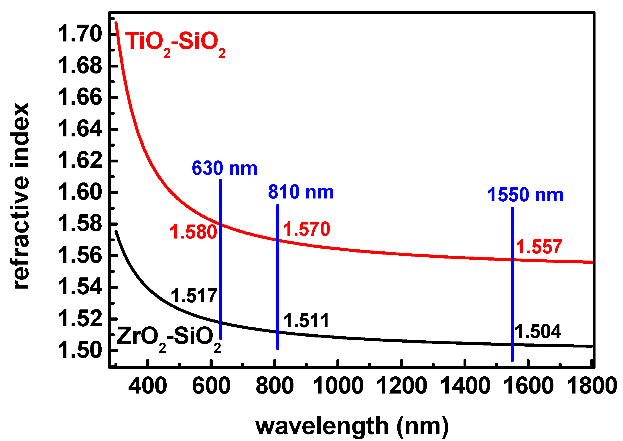
| Wavelength (nm) | n (TiO2–SiO2) | n (ZrO2–SiO2) | ∆n |
|---|---|---|---|
| 630 | 1.580 | 1.517 | 6.3 × 10⁻² |
| 810 | 1.570 | 1.511 | 5.9 × 10⁻² |
| 1550 | 1.557 | 1.504 | 5.3 × 10⁻² |
| Wavelength (nm) | n (TiO2–SiO2) | n (Soda Lime Glass) | ∆n |
|---|---|---|---|
| 630 | 1.580 | 1.522 | 5.8 × 10⁻² |
| 810 | 1.570 | 1.517 | 5.3 × 10⁻² |
| 1550 | 1.557 | 1.507 | 5.0 × 10⁻² |
| Wavelength (nm) | Г1 (Surrounded by Air) | Г2 (Surrounded by Cladding) |
|---|---|---|
| 630 | 0.999 | 0.998 |
| 810 | 0.998 | 0.996 |
| 1550 | 0.980 | 0.976 |
Publisher’s Note: MDPI stays neutral with regard to jurisdictional claims in published maps and institutional affiliations. |
© 2021 by the authors. Licensee MDPI, Basel, Switzerland. This article is an open access article distributed under the terms and conditions of the Creative Commons Attribution (CC BY) license (https://creativecommons.org/licenses/by/4.0/).
Share and Cite
Royon, M.; Jamon, D.; Blanchet, T.; Royer, F.; Vocanson, F.; Marin, E.; Morana, A.; Boukenter, A.; Ouerdane, Y.; Jourlin, Y.; et al. Sol–Gel Waveguide-Based Sensor for Structural Health Monitoring on Large Surfaces in Aerospace Domain. Aerospace 2021, 8, 109. https://doi.org/10.3390/aerospace8040109
Royon M, Jamon D, Blanchet T, Royer F, Vocanson F, Marin E, Morana A, Boukenter A, Ouerdane Y, Jourlin Y, et al. Sol–Gel Waveguide-Based Sensor for Structural Health Monitoring on Large Surfaces in Aerospace Domain. Aerospace. 2021; 8(4):109. https://doi.org/10.3390/aerospace8040109
Chicago/Turabian StyleRoyon, Maxime, Damien Jamon, Thomas Blanchet, François Royer, Francis Vocanson, Emmanuel Marin, Adriana Morana, Aziz Boukenter, Youcef Ouerdane, Yves Jourlin, and et al. 2021. "Sol–Gel Waveguide-Based Sensor for Structural Health Monitoring on Large Surfaces in Aerospace Domain" Aerospace 8, no. 4: 109. https://doi.org/10.3390/aerospace8040109