Article

The Miniature Optical Communication Transceiver—A Compact, Power-Efficient Lasercom System for Deep Space Nanosatellites

1
Precision Space Systems Laboratory (PSSL), Department of Mechanical and Aerospace Engineering, University of Florida (UF), Gainesville, FL 32611, USA
2
Space Telecommunications Astronomy and Radiation (STAR) Lab, Massachusetts Institute of Technology (MIT), Cambridge, MA 02139, USA
*
Author to whom correspondence should be addressed.
Aerospace 2019, 6(1), 2; https://doi.org/10.3390/aerospace6010002
Submission received: 28 November 2018 / Revised: 22 December 2018 / Accepted: 24 December 2018 / Published: 31 December 2018
(This article belongs to the Special Issue Space-based Laser Communications)

Abstract

:
Optical communication is becoming more prevalent in orbit due to the need for increased data throughput. Nanosatellites, which are satellites that typically weigh less than 10 kg, are also becoming more common due to lower launch costs that enable the rapid testing of technology in a space environment. Nanosatellites are cheaper to launch than their larger counterparts and may be a viable option for communicating beyond Earth’s orbit, but have strict Size, Weight, and Power (SWaP) requirements. The Miniature Optical Communication Transceiver (MOCT) is a compact optical transceiver designed to provide modest data rates to SWaP constrained platforms, like nanosatellites. This paper will cover the optical amplifier characterization and simulated performance of the MOCT amplifier design that produces 1 kW peak power pulses and closes three optical links which include Low Earth Orbit (LEO) to Earth, LEO to LEO, and Moon to Earth. Additionally, a benchtop version of the amplifier design was constructed and was able to produce amplified pulses with 1.37 W peak power, including a 35.7% transmit optics loss, at a pump power of 500 mW. Finally, the modulator, seed laser, amplifier, receiver, and time-to-digital converter were all used together to measure the Bit Error Ratio (BER), which was 0.00257 for a received optical peak power of 176 nW.

Graphical Abstract

1. Introduction

1.1. Background

Large amounts of data is being collected on satellites due to advancements in technology such as high resolution and multispectral imagers. High bandwidth communication is needed in space to transfer the collected data to Earth or other satellites where the data can be processed and utilized. Additionally, satellite missions are increasingly taking place outside of Earth’s orbit to explore other planets and celestial bodies. These interplanetary satellite missions will likely have limited communication link opportunities and need to transfer as much data as possible during these windows.
Small satellites, which are satellites with a mass less than ∼500 kg, can be used to fulfill these deep space missions. Small satellites have lower launch costs than larger satellites, since the launch cost increases with increasing satellite mass. Nanosatellites, which are satellites with a mass less than ∼10 kg, are a subset of small satellites. Nanosatellites have even lower launch costs and can be deployed into satellite constellations for large scale sensor acquisition and communication networks. Due to their small form factor, nanosatellites have strict Size, Weight, and Power (SWaP) requirements.
Optical frequencies diverge less than radio frequencies, which enables optical signals to be collimated into a tighter transmitted beam. When utilizing optical frequencies for communication, the transmitted beam can maintain higher intensities for a longer distance and the receiver can capture a larger fraction of the transmitted signal. Optical sensor technology like avalanche photodetectors (APDs) and Gieger-mode APDs enable the detection of ∼100 photons down to a single photon. As a result, optical communication can have lower required transmitter power at the cost of stricter pointing requirements.
The Lunar Laser Communication Demonstration (LLCD) was conducted on NASA’s Lunar Atmosphere and Dust Environment Explorer (LADEE) satellite that launched in late 2013 [1]. The LLCD payload demonstrated optical communication in the 1.5 μ m band utilizing pulse position modulation (PPM) with 16 slots (16-PPM) to downlink data from the moon to a receiver on Earth at 622 Mbps [1]. The uplink from the optical ground terminal on Earth utilized 4-PPM to uplink data at 20 Mbps to LLCD [1]. LADEE was a small satellite that weighed 383 kg at launch and the entire spacecraft consumed 295 W of power during its mission [2]. The LLCD space instrument had a mass of 32.8 kg and consumed 136.5 W during communication activities [2]. Most of this power was used for precision beam pointing.
The Micius Coherent Laser Communication Demonstration (MCLCD) is another small satellite free space optical link that was demonstrated on the Micius Quantum Science Satellite [3]. This 635 kg small satellite [4] was able to achieve a downlink with a data rate of 5.12 Gbps from Low Earth Orbit (LEO) to an optical ground facility [3]. As opposed to LLCD which used PPM, MCLCD utilized Differential Phase Shift Keying (DPSK), where the data is encoded with a phase modulator on a 1550 nm optical carrier [3]. The uplink from the optical ground facility to MCLCD achieved a data rate of 20 Mbps by utilizing 16-PPM and a 1064 nm optical signal [3].
The Miniature Optical Communication Transceiver (MOCT) is a lasercom system being developed by the Precision Space Systems Laboratory (PSSL) at the University of Florida. MOCT aims to enable pulsed optical communication on a nanosatellite platform at lunar distances and closer. Since MOCT is designed for a SWaP constrained platform, it can also be used to provide power efficient, long distance optical communication on larger satellites and free up SWaP resources to be used by other spacecraft subsystems.

1.2. Mission Links

To create a design space for MOCT, three optical link scenarios were investigated: Moon to Earth, LEO crosslink, and LEO to Earth. These links could be incorporated into a nanosatellite optical communication network that could relay information around Earth and as far as the Moon. Furthermore, these links could be adapted for other astronomical bodies (i.e., Mars) so lasercom could be utilized throughout the solar system, where power efficiency is desirable and communication windows are short.
A link equation is used to predict how much of the transmitted signal is captured by the receiver. Equation (1) is the optical link equation that was used to determine the power at a distant receiver from the MOCT transmitter. Equation (1) shares many similarities to link Equation (2.2-1) in [5] and was derived into this form in [6]. The terms in Equation (1) are all in decibels (dB), which is logarithmically scaled. In Equation (1), P r x is the received peak power, P t x is the transmitted peak power, G r x is the transmitter gain, G r x is the receiver gain, and L r a n g e is the range loss. Additionally, η t x is the transmitter optical efficiency, η a t m is the atmospheric transmission efficiency, η r x is the receiver optical efficiency, T p o i n t is the transmitter pointing gain, and R p o i n t is the receiver pointing loss:
P r x = P t x + G t x + G r x + L r a n g e + η t x + η a t m + η r x + T p o i n t + R p o i n t
By using Equation (1) and constraining the receiver peak power to be 200 nW (100 nW with 3 dB margin), the required transmitter peak power was calculated for each link scenario. The required transmitter peak power can be seen in Table 1 with the selected transmitter and receiver sizes used in the link scenario. The maximum required transmitter peak power and design goal for MOCT is 1 kW. Additional detail on the optical link parameters, terms, and equations used for the MOCT link senarios can be found in Appendix A.1.

1.3. Pulse Position Modulation

The modulation scheme selected for MOCT is PPM, since PPM encodes several bits of data with every pulse transmitted. In PPM, the time of arrival of a pulse carries the information being transmitted. When the receiver captures a pulse, the arrival time is compared with time windows called slots that each map to a symbol, S N . The duration of a slot is called the slot width, τ . The number of slots is denoted as M, where M = 2 n and n corresponds to the number of bits that each symbol (slot) encodes. The guard time, T g , is the minimum time between pulses. The guard time is often limited by the transmitter producing enough power for the link, however, it can also be limited by other systems on the transmitter or receiver. An example of PPM modulation for two consecutive symbols ( S N and S N + 1 ) can be seen in Figure 1. Utilizing PPM with photo-counting receiver technology (i.e., APDs) reduces the required transmitter power and decreases the required SWaP on the satellite as a result [7].
The data rate for PPM is D P P M and can be seen in Equation (2). Longer slot widths and longer guard times correspond to lower PPM data rates. The number of slots, M, can be selected to maximize the data rate for a given τ and T g . Both τ and T g should be kept as short as the system will allow to help maximize the data rate.
D P P M = log 2 ( M ) M τ + T g
Other design considerations that can conflict with maximizing the PPM data rate include efficiently generating the required transmitter power and achieving a low Bit Error Ratio (BER). The BER is the total number bit errors divided by the total number of transmitted bits. Longer slot widths are associated with a lower BER. Using a longer guard time allows more time for the transmitter to amplify the pulse, which reduces the required optical pump power and power consumption for an optical amplifier.

1.4. MOCT Architecture

The Miniature Optical Communication Transceiver is a lasercom system capable of both transmitting and receiving optical pulses. This system includes a modulator, transmit channel, and receive channel. The transmit channel is composed of a seed laser and optical amplifier and the receive channel is composed of an Avalanche Photodetector (APD) and a Time-to-Digital Converter (TDC). The MOCT design scope does not include the transmit optics to collimate the outgoing pulse, the receive optics to capture an optical pulse, nor the precision pointing system for the transmitted beam. These non-trival elements would need to be integrated with MOCT in order to utilize MOCT on a nanosatellite. A block diagram of the MOCT architecture can be seen in Figure 2.
When the spacecraft wants to transmit data over an optical link to a distant receiver, the spacecraft sends the modulator the data string to be transmitted. The modulator is a novel software defined pulse modulator (SDPM) implemented on a Microsemi SmartFusion2 [8] field programmable gate array (FPGA) and utilizes a Microsemi Chip Scale Atomic Clock (CSAC) [9] as the reference oscillator. The modulator takes the data string and encodes it using pulse position modulation (PPM) by varying the time delay between generated electrical pulses. Two 2.5 GHz Serializer/Deserializer (SERDES) hardware modules onboard the FPGA, offset from each other by a calibrated Delay Locked Loop (DLL), form the physical layer of the modulator. The modulator is able to set τ and T g with a resolution of 400 ps, and control the pulse width with 1 ps increments. The rising and falling edges of the modulated pulses have a random time error (jitter) of less than 30 ps. As opposed the modulators commonly used in communication that rely on fast slot clocks with high power consumption to make slots, the MOCT modulator utilizes timing delays.
The electrical pulses from the modulator are sent to the pulse driver, which converts the electrical pulses into optical pulses. The pulse driver is composed of a seed laser and a custom designed pulse diver circuit board called the Fast Laser Advanced Switching High-Frequency Emitter (FLASHE). The seed laser is a 1531 n m laser capable of delivering up to 40 mW of power. FLASHE utilizes Gallium-Nitride (GaN) field-effect transistors (FETs) for radiation resilience. The circuit configuration of the FETs on FLASHE enable the seed laser to produce optical pulses as short as ∼100 ps. Nominally, the seed pulses on MOCT will have a pulse width of ∼1 ns and peak power of ∼5 mW.
The seed pulses are coupled into an optical amplifier capable of amplifying the pulse to peak powers of ∼1 kW without significant distortion the pulse shape. The optical amplifier is a single stage, erbium doped fiber amplifier (EDFA) in a master oscillator power fiber amplifier (MOPFA) configuration. The optical amplifier has a single stage with a counter-propagating (backwards) ∼980 nm pump laser configuration. The pump power can be adjusted to provide only enough amplification to close an optical link. The erbium doped fiber type used is Liekki ER80-8/125 [10], which has a high doping concentration (∼80 dB/m) that enables short lengths of fiber that have high gain and reduce nonlinear effects like Stimulated Raman Scattering (SRS), Stimulated Brillouin Scattering (SBS), and Four-Wave Mixing (FWM) [10]. Additionally, this fiber has a large single mode core for ∼1.5 μ m light that also makes coupling the pump light easier. After the optical amplifier, the amplified pulse is sent to the distant receiver through the transmit optics.
When the spacecraft captures an optical pulse from a distant transmitter in the receive optics, the optical pulse is detected by the APD. The APD converts the captured optical pulse into an electrical pulse. A transimpedance amplifier (TIA) at the exit of the APD helps this detector achieve a 1 GHz bandwidth. Temperature control via a thermoelectric cooler (TEC) and an adjustable reverse bias voltage are used on the APD to control the detector gain. Two programmable gain amplifiers (PGA) are used after the TIA that can each be adjusted to attenuate the electrical pulse by a maximum of −12 dB or amplify the electrical pulse up to 52 dB. The PGAs enable the detector to have a large dynamic range of received optical power. The entire detector and circuitry fits on a custom board design called Near-infrared Optical detection with Variable Amplification (NOVA) which is a 30 mm × 30 mm printed circuit board that consumes ∼1 W of power during detection. The detector output is a differential pair and is routed to the comparator on the front end of the TDC.
The TDC time stamps the arrival of each detected pulse from the APD. The comparator on the front end of the TDC takes the analog differential pair from the APD, compares it to an adjustable threshold, and outputs a low-voltage differential signaling (LVDS) pair to the TDC. When the APD output voltage is below the threshold, the comparator outputs a logical false on the LVDS pair. When the APD output voltage is greater than the threshold, the comparator outputs a logical true on the LVDS pair. The TDC being used on MOCT is the AMS TDC-GPX2 and is capable of 20 ps single shot timing accuracy [11]. For single edge thresholding, the TDC records the moment in time when the LVDS pair transitions from a logical false to a logical true. This time stamp corresponds to when the rising edge of the APD is greater that the comparator threshold. The falling edge of the APD signal can simultaneously be timed with the another channel on the same TDC-GPX2 chip. The event that is timed for the falling edge is when the comparator output transitions from logical true to logical false. The rising and falling edge time can be averaged to reduce arrival time errors associated with optical power fluctuations. The time stamp of the optical pulse arrival is sent from the TDC to the modulator for decoding. Since the TDC measures the arrival of the optical pulse as a moment in time, the modulator only has to decode which PPM slot the time stamp is in and the optical pulse width can be greater than the PPM slot width. The modulator then sends the decoded receiver data to the spacecraft bus.
Together, all of the MOCT components work congruently to provide power efficient, pulsed optical communication on a nanosatellite platform at lunar distances. Utilizing PPM for optical communication also helps MOCT achieve a power efficient communication link. Compared to other lasercom mission that design for high data rates (>1 Gbps), MOCT intends to achieve modest data rates of ∼40 Mbps in a compact, low power consumption platform.

2. Materials and Methods

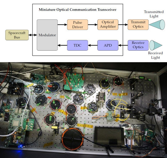
2.1. MOCT Laboratory Hardware

The MOCT laboratory hardware incorporates the same components as the MOCT space hardware, which includes the modulator, pulse driver, optical amplifier, APD, and TDC. These components are in a modular configuration that allows component performance to be assessed both individually and in groups. The MOCT hardware on a satellite can be designed to fit in a nanosatellite package, while the modular connections on the laboratory hardware, needed to evaluate components individually, would be eliminated to increase efficiency for volume, weight, optical transmission.

2.1.1. Modulator

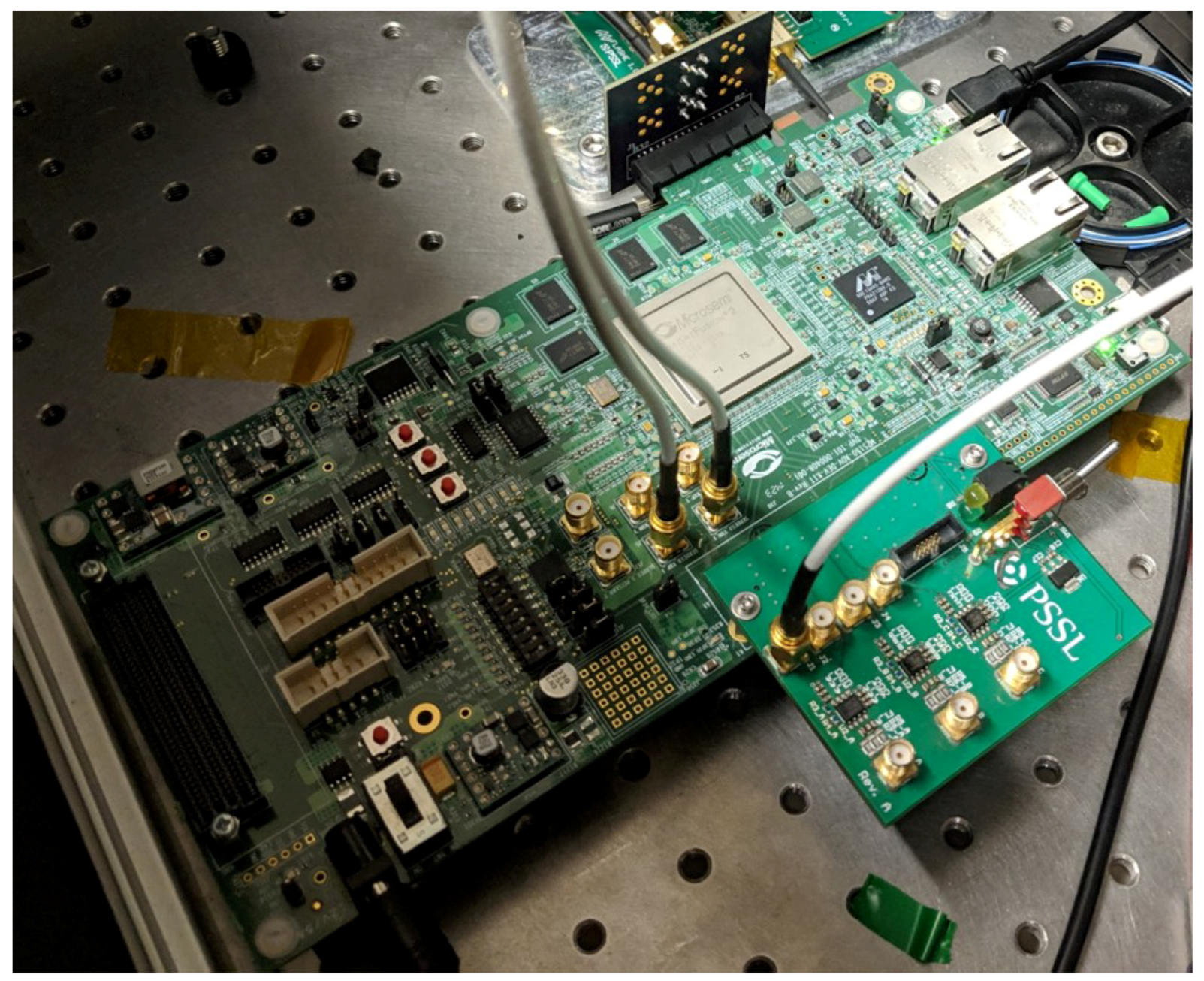
A novel PPM modulator, with precise pulse duration control, has been developed for MOCT. The FPGA being used for the modulator on a Microsemi development board can be seen in Figure 3. The seed laser driver described later in this paper (Section 2.1.2) requires two digital signals with an adjustable phase difference. The signals also need a high time resolution to produce short time slots for the PPM modulation. Our current implementation uses two of the SERDES hardware modules of the Smartfusion 2 FPGA (Microsemi Corporation, Aliso Viejo, CA, USA). The two SERDES modules are synchronized with a single clock, and the phase of clock for the second SERDES can be adjusted with a variable delay chain. The PPM symbols to be transmitted are first split in a counter value and SERDES word position, then a second logic block generates 20-bit words for the SERDES modules. The resulting modulator has a resolution of 400 ps for the PPM slots because of the 2.5 GHz maximum SERDES frequency. The pulse duration is adjustable down to 12 ps increments by utilizing the delay chain resolution. In addition, the 20-bit words sent to the SERDES modules allow 400 ps adjustments. The additional jitter introduced by the delay chain is partially filtered by the SERDES module integrated Phase Locked Loops (PLLs). The resulting modulator is highly configurable: the guard time, the slot duration and the pulse duration can be adjusted. Data rate of up to 1.25 Gbps can be achieved with PPM4 at 625 MHz symbol rate, but such data throughputs are limited by the seed laser and the available optical power from the EDFA. Since all the timing circuitry is implemented inside the FPGA, and no external analog timing adjustments are required, the modulator can be efficiently implemented at no PCB area cost while using few FPGA resources. The power consumption of the modulator, which includes both the FPGA and development board, was measured to be 7.32 W. When the development board is powered on, it also powers USB ports, Ethernet ports, and other features that would not be used on a space version of the modulator. However, some additional memory and processors will be needed so the modulator as a whole is expected to consume at least 5 W.

2.1.2. Seed Laser

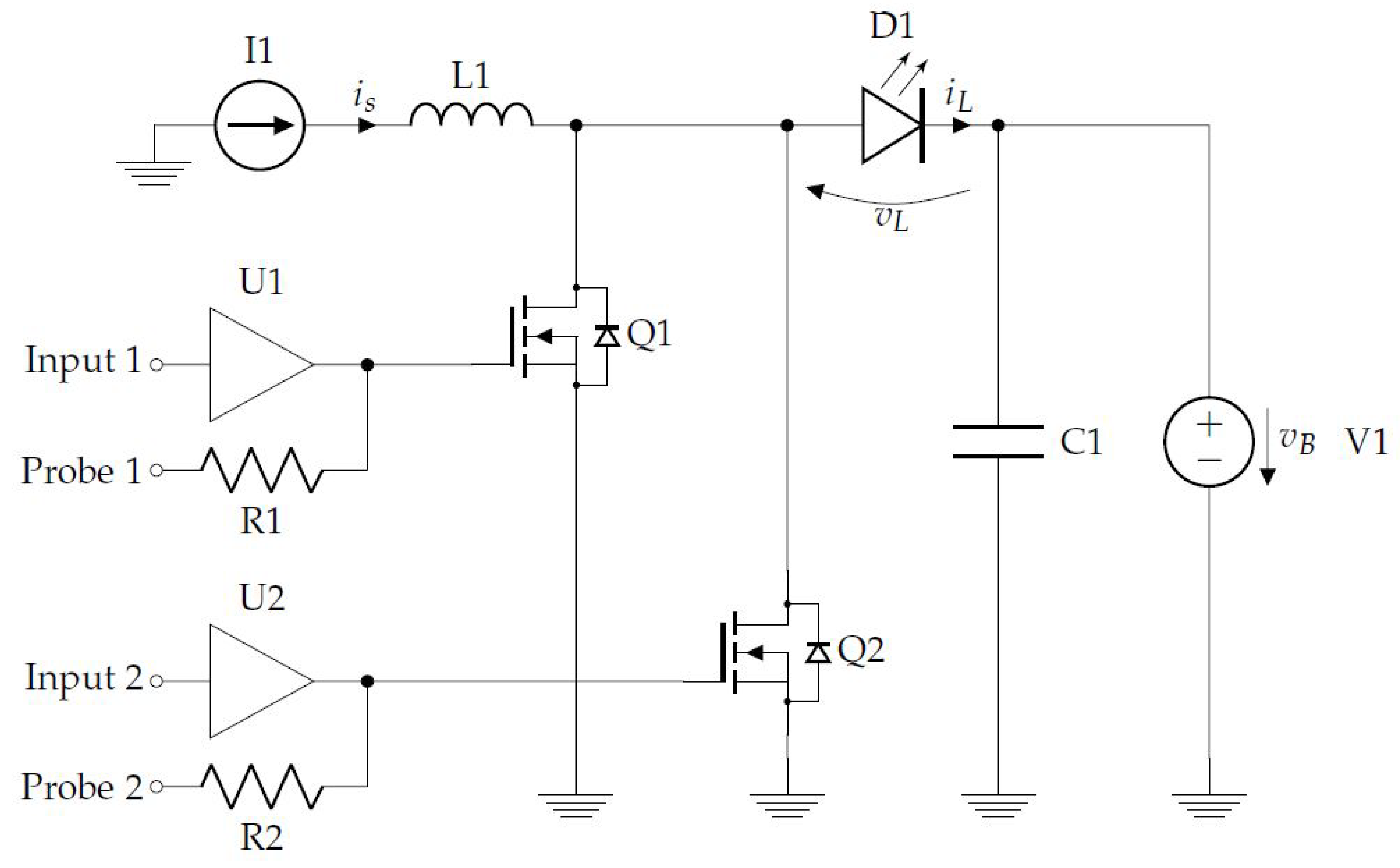
The Fast Laser Advanced Switching High-Frequency Emitter (FLASHE), a 1531 nm seed laser and pulse driver, emits stable pulses as short as 100 ps [12]. Its output is the pre-amplified data signal, which goes to the optical amplifier. FLASHE receives two digital signals containing the PPM data string from the modulator, with the second signal inverted and delayed from the first. The pulse duration is set by the time from the first input’s falling edge to the second input’s rising edge. The digital inputs are sent to two Field Effect Transistors (FETs), which must both be open to send current to the seed laser. The double FET configuration can be seen in the overall circuit design in Figure 4 as Q1 and Q2.
The circuit was designed to pulse a laser (D1) at 50 MHz with up to 500 mA of current (from I1). The threshold current to emit light from the selected laser is 50 mA. The design of FLASHE keeps the current just below the population inversion threshold in between pulses, and jumps above the threshold when emitting light. The negative bias voltage (V1) at the cathode of the laser enables the voltage across the laser to be just below the threshold value. The application of a constant bias reduces the amount of voltage change required to pulse, therefore reducing the rise time. Particular attention was given to decoupling the laser bias to ensure that the bias voltage supply conserved a low impedance at high frequencies. Very low impedance capacitors (C1) have been incorporated to maintain an impedance below 1 Ohm up to 10 GHz.
The design of FLASHE is novel because it incorporates two slower transistors instead of one fast transistor and removes the need for a radio-frequency amplifier. Both transistors are operated in linear mode (similar to switching power supplies) which enables lower power consumption. However, having two switches increases jitter error [12]. In addition, FLASHE uses gain-switching, which adjusts the laser gain by abruptly providing and removing pump power [12,13]. Incorporating both gain-switching and two transistors allows FLASHE to generate pulses down to 100 ps (full width half maximum) without requiring radio frequency electronics.
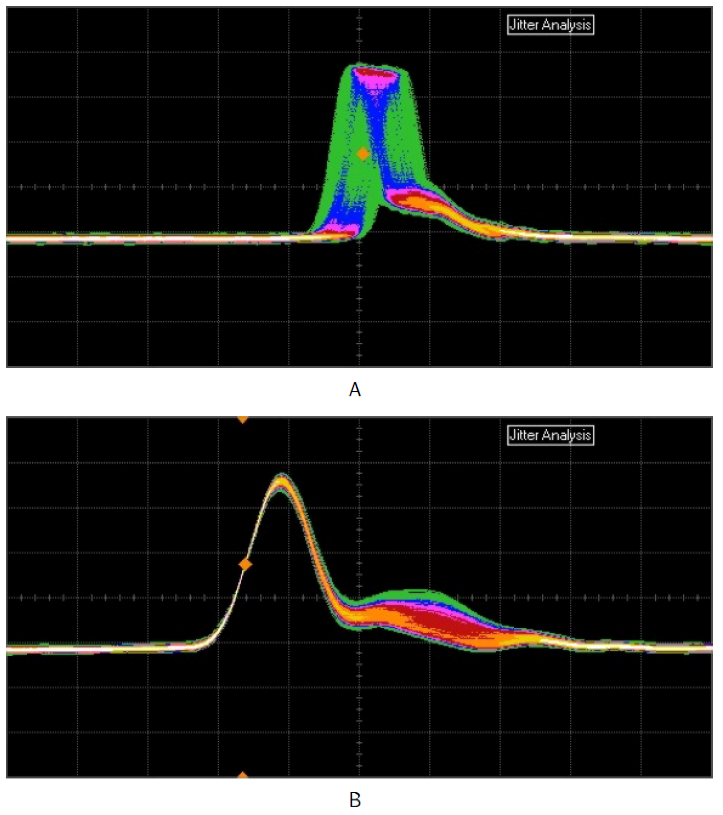
Capable of emitting pulses in the nanosecond range down to hundreds of picoseconds, the shortest pulse FLASHE has demonstrated is 100 ps as seen in Figure 5 [12]. Measured jitter is between 25 ps to 200 ps, which is mainly dependant on the modulation type and the modulator used [12]. The optical peak power range is from ∼1 to 40 mW. Both the duration and the pulse amplitude can be adjusted to achieve a desired pulse shape.
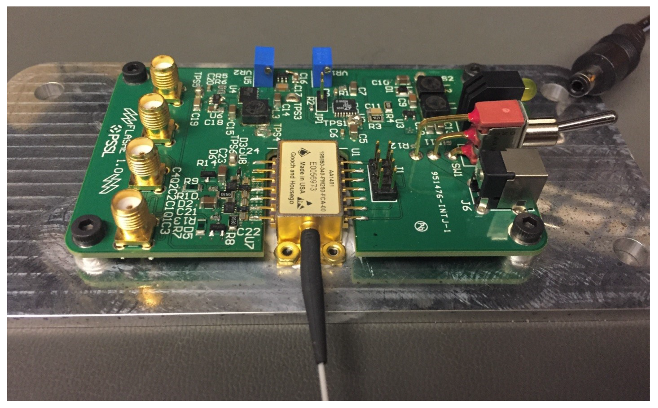
There are two versions of the laser driver: FLASHE 1.0, made for in-lab experiments and testing, and FLASHE 2.0, designed as an engineering unit and is currently being fabricated and tested. The power consumption for FLASHE 1.0 has been measured to be 1.3 W. A large portion of that power is dedicated to the current source. In comparison, the FET driver average consumption is estimated to be less than 5 mW. The power consumption of FLASHE 2.0 is expected to be lower due to voltage reductions for its linear current source. A DC/DC current source could further reduce power consumption, below 200 mW for the complete laser driver. The printed circuit board (PCB) for FLASHE 1.0, which can be seen in Figure 6, is approximately 50 mm × 80 mm. The 1531 nm laser has dimensions of 13 mm × 48 mm × 9.5 mm, which includes the black fiber cover. The Printed Circuit Board (PCB) area utilized for the current source and switches on FLASHE 2.0 is less than 2 cm 2 . This reduction in PCB area makes FLASHE 2.0 suitable for a nanosatellite platform.

2.1.3. Optical Amplifier

The optical amplifier is responsible for amplifying the 1.5 μ m seed laser pulses to a high enough peak power in order to be detected by the distant receiver. For MOCT, the optical amplifier is an erbium doped fiber amplifier (EDFA) in a master oscillator power fiber amplifier (MOPFA) configuration. The continuous wave (CW) ∼980 nm pump laser is coupled with the erbium doped fiber and stores energy via stimulated absorption with the erbium ions. When the seed laser pulse is emitted into the erbium doped fiber that has energy stored in the erbium ions, the seed laser pulse is amplified via stimulated emission. The gain from the EDFA is controlled by how much pump power is coupled into the fiber and how long the erbium doped fiber is charged between seed pulses. In general, higher pump powers and a longer time between pulses are associated with higher amplification (within some physical limitations of the particular amplifier) than lower pump powers and a shorter time between pulses. One characteristic of EDFAs is that they are able to amplify pulses with very little temporal distortions on the original seed pulse.
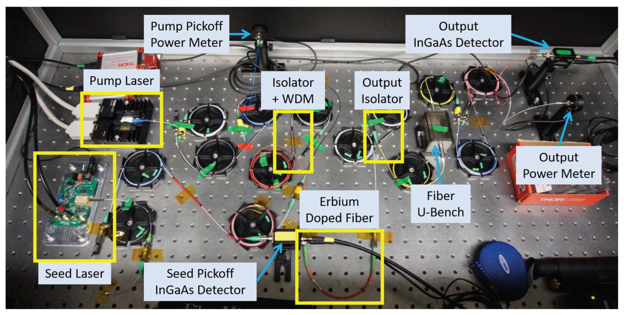
For testing the optical amplifier MOCT hardware in the laboratory environment, the Fiber Laser Amplifier Testbed (FLAT) was constructed and developed. A picture of the FLAT can be seen in 
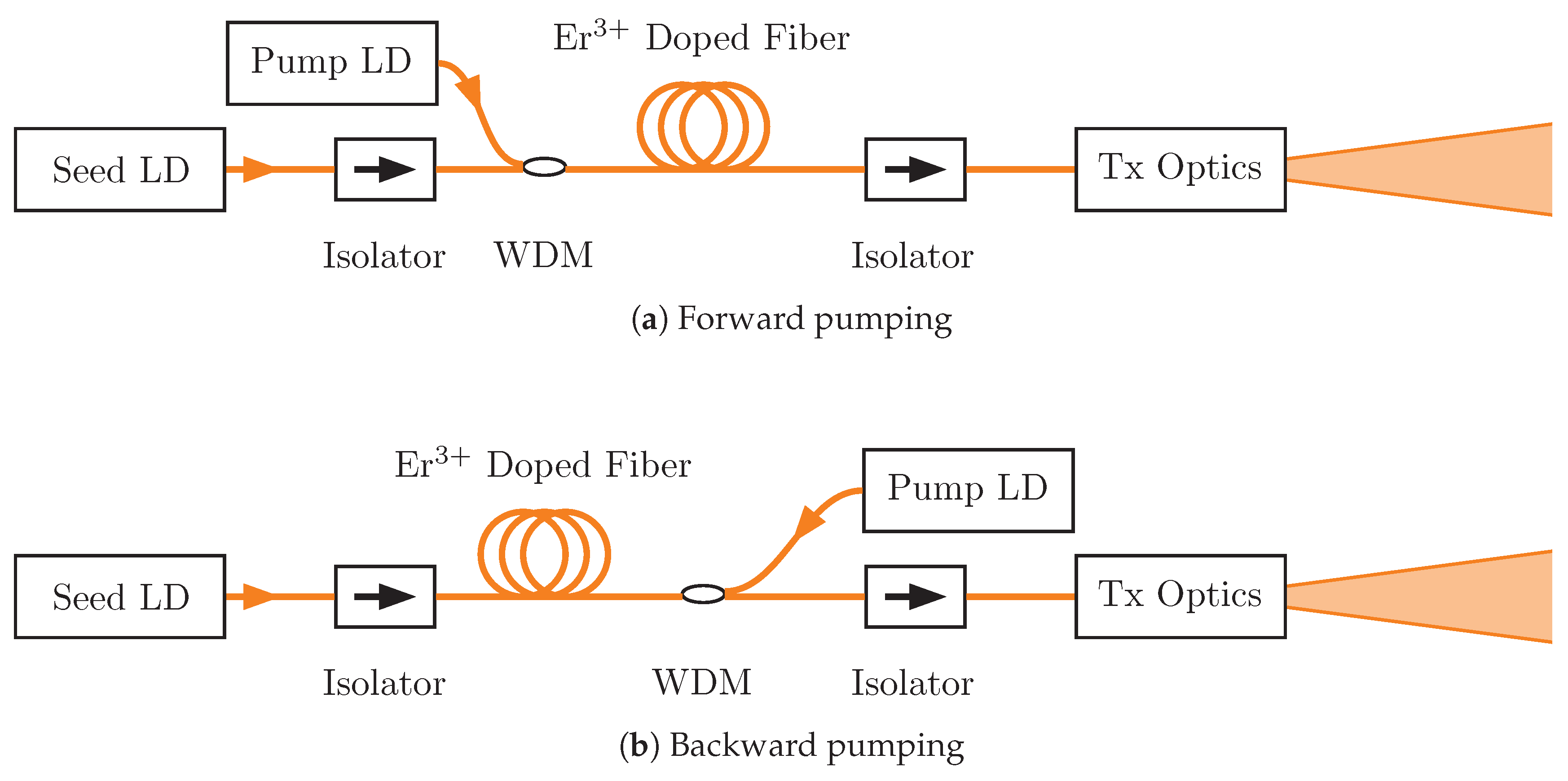
Figure 7. The FLAT is the optical amplifier in a spacious configuration, utilizing FC/APC connectors throughout the testbed to rapidly test different amplifier configurations. Additionally, fiber beam splitters were used in conjunction with a PIN diode and power meter to monitor the seed laser and pump laser signals into the optical amplifier. A 976 nm pump laser with a maximum output power of 600 mW CW was selected and used in a forward pump configuration as seen in Figure 8a. This configuration was used in the optical amplifier characterization testing where the power damage threshold is ∼300 mW CW. A backward pump configuration, as seen in Figure 8b, has a higher gain than forward pumping for the same pump power at the cost of more forward Amplified Spontaneous Emission (ASE). Forward ASE is a band of optical signals near the wavelength of the seed laser, so it can be difficult to reject with filtering, and therefore increases transmitted optical noise. When the benchtop transceiver testing was conducted, a Wave Division Multiplexer (WDM) with higher power rated connectors was available, allowing this demonstration to implement a backwards pumping configuration. For a space mission, permanent fiber spliced connections and free-space components can be used, which can both greatly increase the optical power damage threshold and enable more pumping configuration freedom. The pump laser currently used on the FLAT has an electrical to optical power efficiency of 35 % and consumes ∼1 W of electrical power. If the same efficiency was on a 4 W pump laser, it would consume 11.4 W of electrical power.
Some other components on the FLAT that would not be present on the MOCT space hardware include the U-Bench and the two output detectors. The U-bench launches the optical signal into free-space, sends the signal through free-space optics, and then couples the resulting optical signal back into the fiber. The U-bench was used the attenuate the amplified optical signal by a known amount until it was within the dynamic range of the output detectors. Both a PIN diode and a calibrated power meter were used with a fiber beam splitter so both the temporal characteristics and average power of the output optical signal could be monitored simultaneously. For testing the MOCT receiver, one of the detectors can be replaced by a collimator to transmit a free-space optical beam at the receiver optics and detector.

2.1.4. Avalanche Photodetector

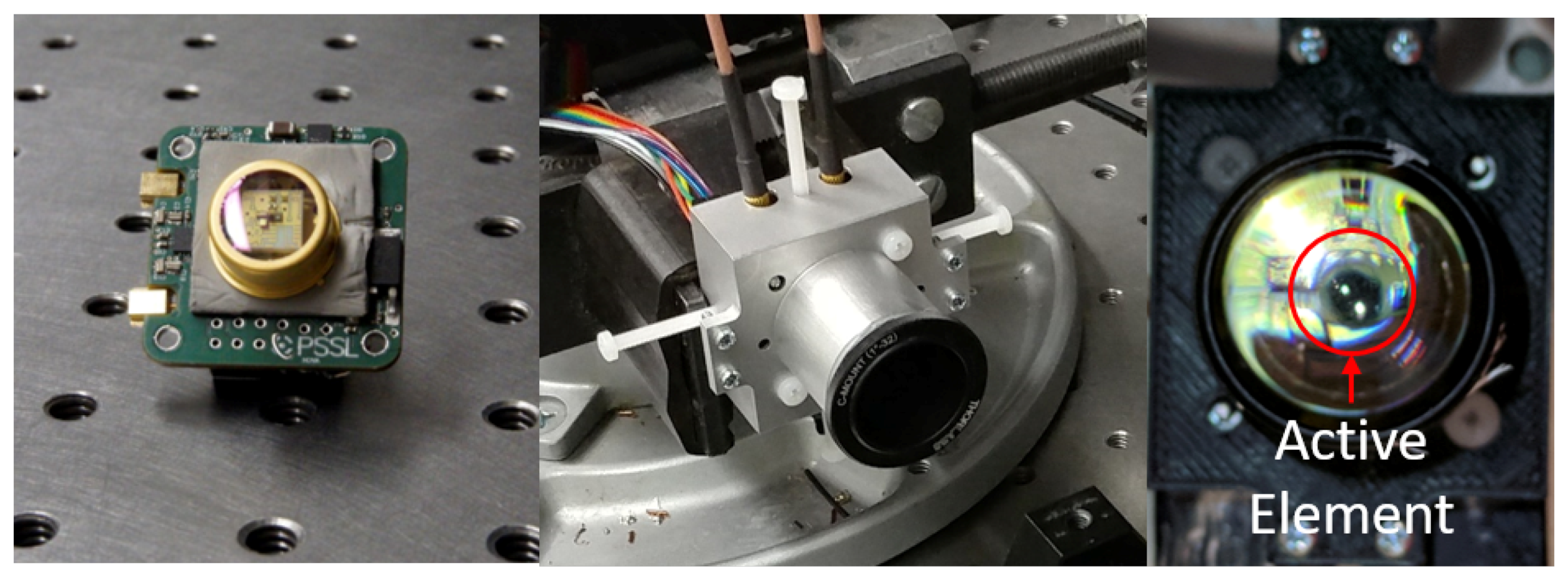
The avalanche photodiode (APD), as seen in Figure 9, is responsible for detecting the 1531 nm optical pulses, and outputting the electrical pulses quickly and efficiently to be time stamped by the time-to-digital converter. The current APD is a Voxtel RIP1 series free-space InGaAs detector (Voxtel, Inc., Beaverton, OR, USA), with a 200 μ m active element and a transimpedance amplifier integrated within the housing to reduce noise and retain its 1 GHz bandwidth. Utilizing two programmable gain amplifiers (PGA) in series, the 30 mm × 30 mm board can perform over a dynamic range of 60 dB while only consuming about 1 W. The APD board interfaces directly with a Raspberry Pi (emulating an FPGA board) via Serial Peripheral Interface (SPI), as well as with a daughter board via AC coupled SubMiniature version A (SMA) cables, which, using a comparator with a digital-to-analog converter configured threshold, sends a digital pulse to the time-to-digital converter board.

2.1.5. Time-to-Digital Converter

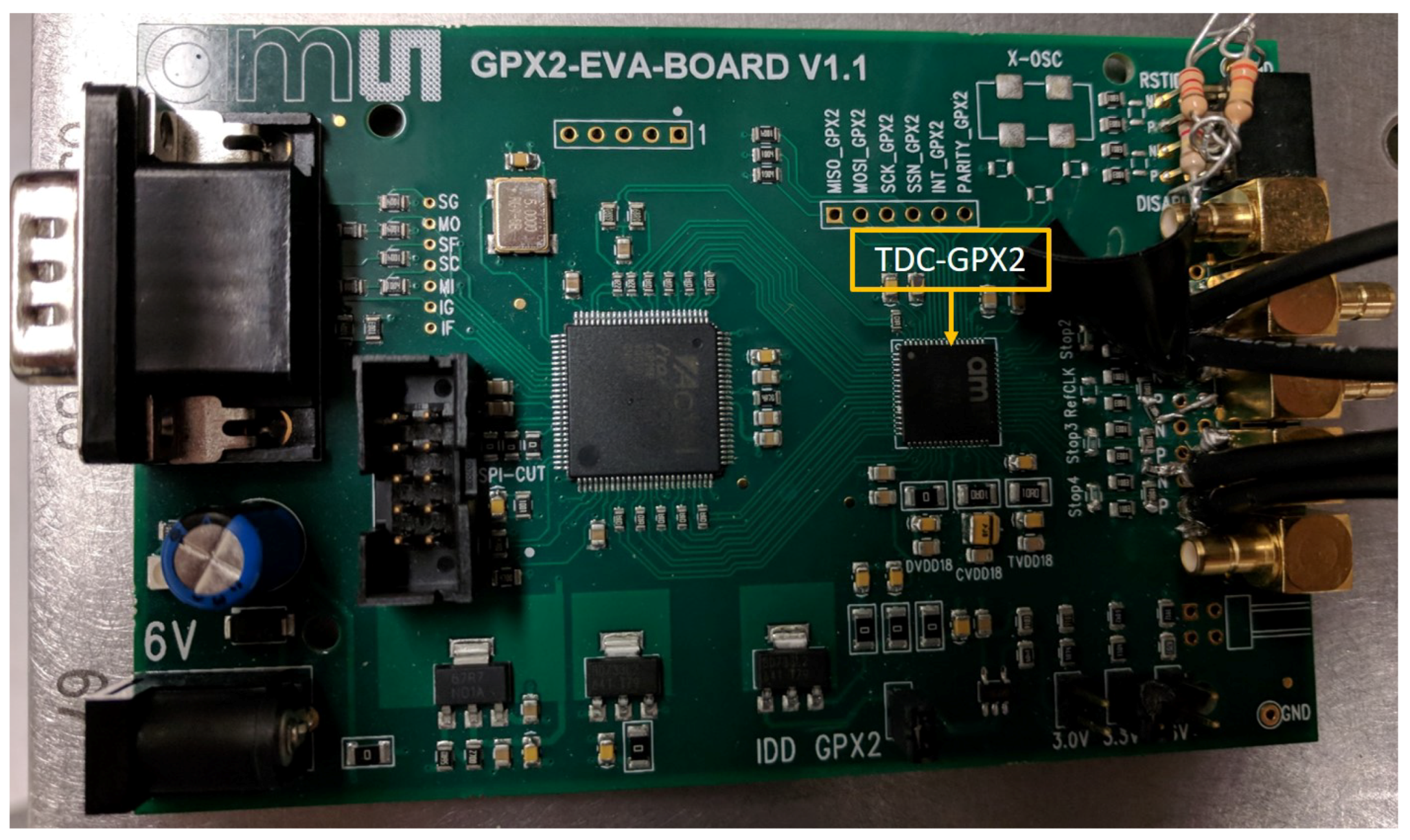
The Time-to-Digital Converter 2 (TDC-GPX2) was selected due to its high data throughput provided by LVDS stop inputs as well as LVDS serial outputs for each channel. Dissipating between 60 mW and 450 mW, the TDC-GPX 2 is capable of combining two channels or using the four individually, with a maximum of 70 megasamples per second for the former and 35 megasamples per second for the latter. The 9 mm × 9 mm chip is located upon a development board, as seen in Figure 10, which is connected directly to the APD daughter board and a laptop via USB. The TDC-GPX2 is capable of 20 ps rms single shot resolution per channel, and the accuracy has been measured to be less than or equal to 40 ps. Currently, for the MOCT receiver, the TDC is on development board that is only able to capture 16 measurement segments consecutively followed by a resting period before collecting more measurements. This development board is the limiting factor; once the TDC-GPX2 chip is on its own PCB, optical pulses can be time stamped continuously.

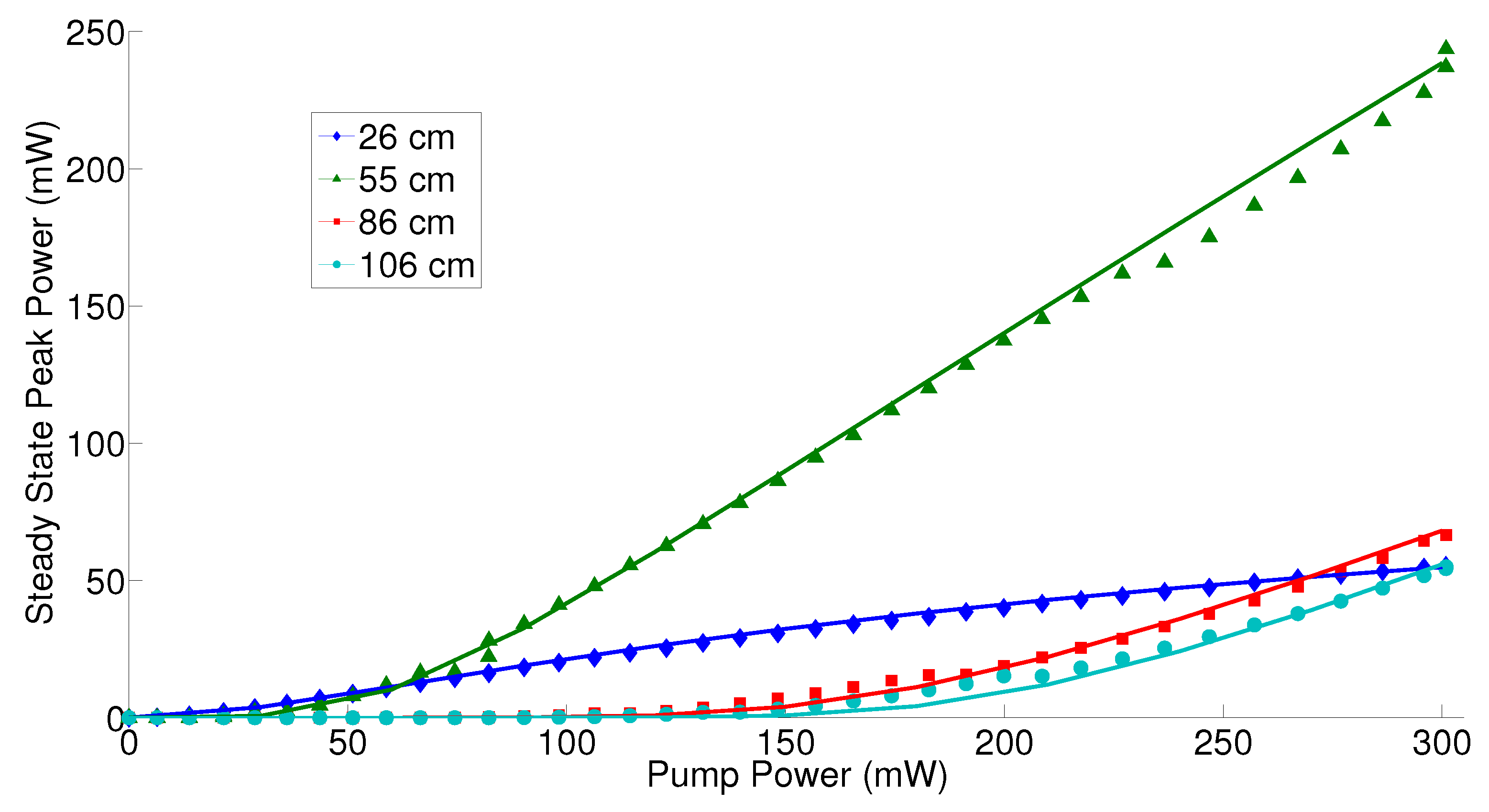
2.2. Optical Amplifier Characterization

The goal of the optical amplifier characterization was to measure the performance of the FLAT as a function of input pump power, for a few lengths of fiber. The results from this experiment could be used to develop a computer model. Finally, the model could be used to make an amplifier design suitable for a SWaP constrained platform.
The regime investigated for the optical amplifier characterization was a fixed pulse string at a repetition rate of 20 MHz. This regime had guard times on the order of what is anticipated for SWaP constrained platforms (∼50 ns) that balance data rate and peak power produced. To capture the limiting case peak power generation for the link, data was recorded after the amplifier output decays to its steady state output (less than a few seconds). The experimental parameters used and ranges can be found in Table 2.
Throughout the measurements, all of the fiber ends were cleaned at every connection and inspected with a fiber microscope. This was done to reduce the risk of fiber damage and to keep coupling losses as low as possible. All of the fiber optics from the pump and seed lasers up to the connector that interfaces with the erbium doped fiber entrance were left connected throughout all experimental runs. Additionally, all of the fiber optics between the output detectors and the connector that interfaces with the exit of the erbium doped fiber also remained connected throughout all experimental runs. The only optical components changed between measurements were the neutral-density (ND) filters on the U-bench, which have low insertion uncertainty, and the erbium doped fiber used for the experimental run. Connecting each erbium doped fiber may have introduced some coupling uncertainties when connected with the entrance and exit connectors. However, they were thoroughly inspected and cleaned before connecting to keep uncertainties low. Even with clean connectors, each fiber may have unique coupling losses at each end from manufacturing differences and different polishing batches.
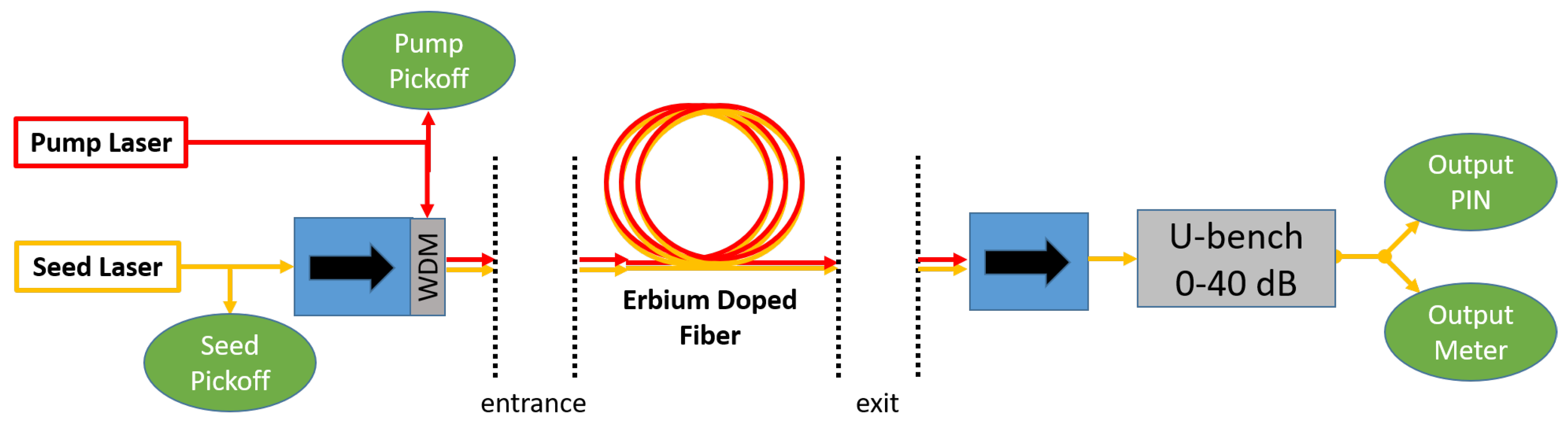
To measure the pump and seed laser signals, a detector was coupled to the connector that would join to the entrance of the erbium doped fiber. Each laser was separately turned on and the powers at the respective pickoffs to the entrance of the erbium doped fiber were measured. These measurements were used to determine the power at the erbium doped fiber entrance without needing to disconnect. The loss for the fiber optics after the exit of the erbium doped fiber was also measured. This loss was measured by directly connecting the fiber optics that were before and after the erbium doped fiber (with no ND filters). Each laser independently emitted light and measurements of the pickoff and the output detectors were recorded. Using the pickoff detector measurements and the calibration relating the pickoff measurements to the power at the erbium doped fiber entrance, the optical loss for each laser on the fiber optics after the erbium doped fiber was calculated. In this calculation, one uncertainty added is the coupling between the two sets of fiber optics, but this is assumed to be small compared to the losses from the exit fiber optics. A diagram of the FLAT characterization setup can be seen in Figure 11.
A dynamic (pulsed), steady-state simulation was developed using the RP Fiber Power software (Version 7, RP Photonics Consulting GmbH, Bad Dürrheim, Germany) [14] to model the performance of the FLAT. The simulation utilized functions built into the RP Fiber Power software to account for optical effects. This dynamic simulation is able to evaluate optical powers along the fiber for a small time step. By combining the evaluated optical powers at every time step, the amplification of an optical pulse can be evaluated. The energy model used is the two level approximation of the erbium ion energy levels. Additionally, homogeneous upconversion (HUC) and pair-induced quenching (PIQ) were also accounted for in this model. The parameters used for HUC are the number of ions are included in the upconversion ion interactions and the upconversion coefficient ( C u p c o n ), which is related to impact that HUC has on the ion energy level populations. For PIQ, the parameters used are the number of ions per cluster and the fraction of the total ions in clusters. The PIQ effects were accounted for by defining separate populations for pairs and single ions and using the PIQ function included in the RP Fiber Power software. Amplified spontaneous emission (ASE) was also accounted for with this software over a spectrum of 1520 nm to 1580 nm. These parameters, except C u p c o n , can be found in Table 3.
In this simulation, a 1531 nm seed pulse is propagated through a single clad, erbium doped fiber core of 7.6 μ m in diameter. The fiber was pumped in the core with a 976 nm laser in a forward pump configuration. Optical signals were assumed to be guided along the fiber core with a Gaussian intensity profile. The doping was assumed to be uniform and contained in the fiber core. A doping concentration of 37 × 10 24 ions/m 3 seemed to fit better than the specification ( 39 × 10 24 ions/m 3 ) for all four fiber lengths. This is acceptable to use since it falls within the 10 % doping concentration uncertainty specified by the manufacturer [15]. The losses of the seed and the pump at the entrance of the erbium fiber were set to be 4 % . The exit loss for the signal was set to be 35.7 % , which is 4 % from the connector plus 31.7 % measured from the output optics. The exit loss of the pump laser used was 99.9 % , which was from the provided isolator data sheet (30 dB) and verified with measurements. These parameters can be found in Table 3. It is important to note for Table 3 that the emission and absorption cross sections were intentionally excluded, since they were not found on public sources. The values used were for the pump and seed wavelengths and were selected from a list in the RP software, which acquired the cross section values from the manufacturer.
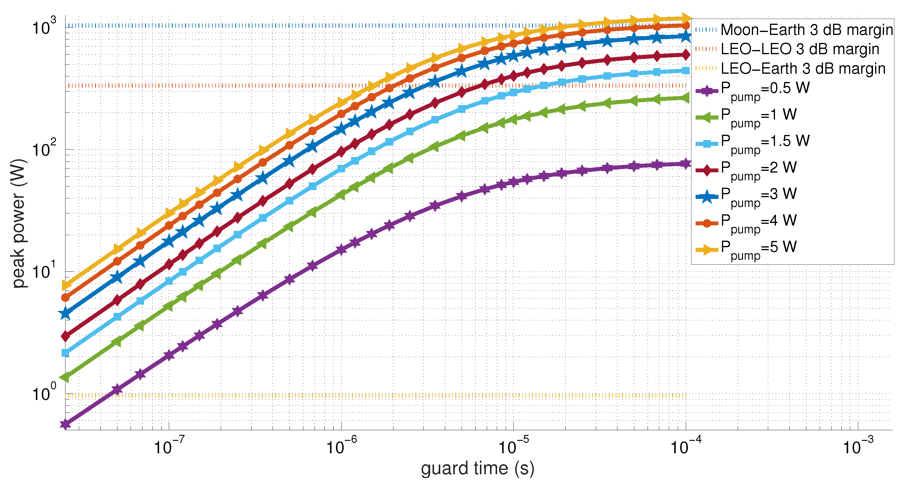
The current EDFA design for MOCT is a single stage with a 4 W maximum pump in a counter propagating configuration. This EDFA design was simulated using the model developed for the FLAT, with modifications for the fiber length, pump power, and pump propagation direction. The pump laser is the only component in this EDFA that consumes electrical power and for a pump laser with an efficiency of 35%, the maximum power consumption is ∼11.5 W. This EDFA is anticipated to amplify 1 ns wide and 5 mW peak seed pulses to 1 kW of peak power at the EDFA output. The pump power can be adjusted to ensure the seed pulse is amplified with only enough margin to close the optical link and reduce power consumption associated with unnecessarily large amplifier gain. The erbium doped fiber is 1.6 m of Liekki ER80-8/125 (nLIGHT, Inc., Vancouver, WA, USA), which has a large single mode core for 1.5 μ m light which makes it easier to couple the pump light and can increase pumping efficiency compared to small cores. This fiber also has a high doping concentration which has high gain per length of fiber (80 dB/m) and enables shorter fiber lengths for a particular gain. Shorter fiber lengths help reduce nonlinear amplifier effects like Stimulated Raman Scattering (SRS), Stimulated Brillouin Scattering (SBS), and Four-Wave Mixing (FWM). The NuPhoton NP3000 series fiber amplifier (NuPhoton Technologies, Inc., Murrieta, CA, USA) is an existing commercial EDFA that has dimensions of 70 mm × 90 mm × 15 mm and weighs ∼0.17 kg. It is believed that the MOCT EDFA would be able to fit in a similar form factor for a nanosatellite mission.

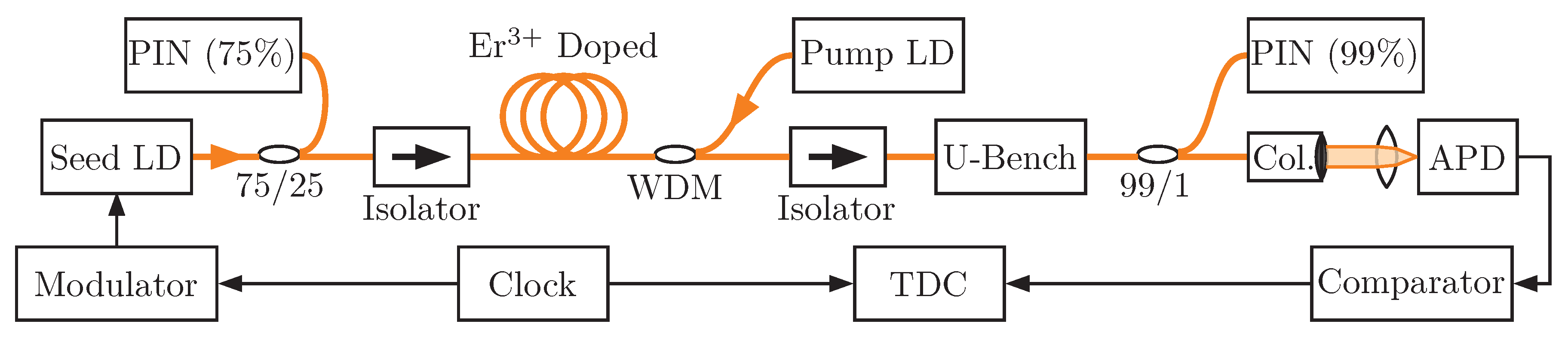
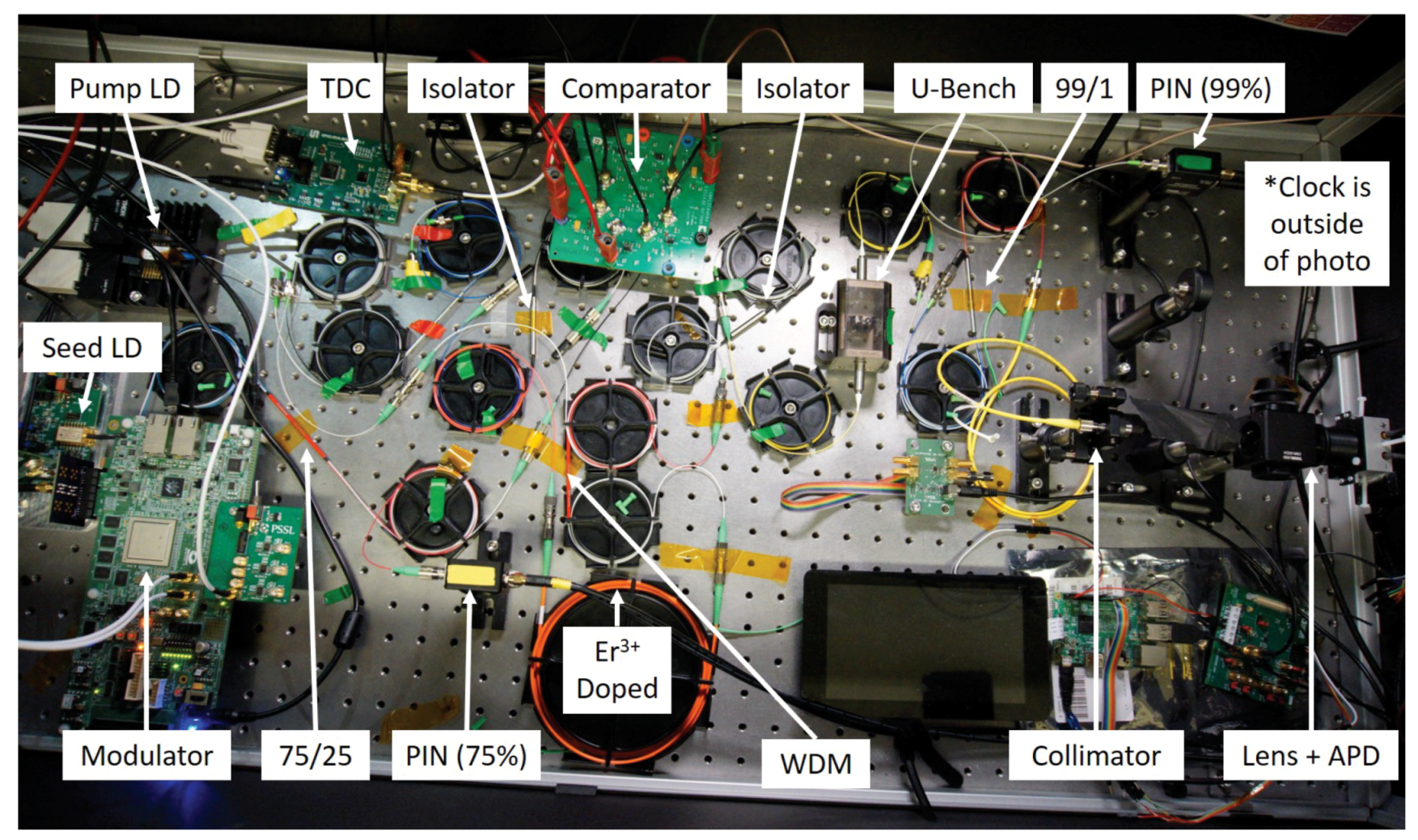
2.3. Benchtop Transceiver Testing

The goals of the benchtop transceiver testing were to determine if the amplifier design can achieve expected amplification and determine the Bit Error Ratio (BER) performance of the transceiver when the APD captures pulses with ∼100 nW of peak power. A 1.6 m erbium doped fiber in a backwards pumping configuration was determined as the amplifier design for MOCT from the results of the optical amplifier characterization. A diagram of the setup can be seen in Figure 12 and picture of the setup can be seen in Figure 13. This latest version of the FLAT has incorporated a collimator, receiver focusing lens, APD, comparator, TDC, Modulator, and a clock in order to test the transceiver hardware. The signals on the PIN diodes and the APD are monitored with an oscilloscope. The TDC sends collected time stamps to a computer via USB cable. It should also be noted that the TDC and the modulator shared a reference oscillator, called the Miniature Atomic Clock, so clock discrepancy is removed.
Some differences from this setup compared with the MOCT design include using a 500 mW pump laser, a seed signal with ∼60 μ W of peak power, and 2.5 ns pulse widths. Even though the power damage threshold of the WDM connectors was increased from the previous FLAT hardware, 500 mW is close to the maximum allowable backward propagating pump power. Splicing all of the fibers together would increase the allowable pump power and a higher power pump could be used. The seed peak power being injected into the erbium doped fiber entrance was measured to be ∼60 μ W and was strong enough to be amplified. Adjustments could be made to hardware settings to increase this if needed. The pulse width was kept at 2.5 ns to avoid signal attenuation due to the oscilloscope’s bandwidth.

2.3.1. Amplifier Verification

The goal of the amplifier verification test was to demonstrate the benchtop amplifier’s capabilities in a configuration similar to the MOCT amplifier design and compare the measured performance with expected performance produced from the optical amplifier simulation. First, the efficiency of the pump laser being injected into the erbium doped fiber was measured to be 72.9%. Second, the efficiency of the 1531 nm signal from the exit of the erbium doped fiber to the output PIN was estimated, after combining a series of measurements, to be 56.5% with no added attenuation on the U-Bench. The fibers were then connected back together and the test was conducted. For this experiment, the collimator, APD, comparator, and TDC were the only components in Figure 12 that were not used.
During the amplifier verification experiment, the pump power was set to zero and the modulator sends a constant pulse string at ∼17.6 MHz (1 pulse every 56 ns) to the seed laser. The pump power was slowly increased until the received signal at the PIN diode was near its maximum and attenuation was added to the U-bench. This process was repeated until 500 mW was indicated by the pump monitor diode (∼10% accuracy). The final attenuation that was added to the U-bench was 30 dB (∼5% uncertainty). At this maximum pump power, the peak power on the PIN diode was recorded, adjusted for attenuation, and compared with the simulation results from the optical amplifier characterization.

2.3.2. BER Measurement

Bit Error Ratio (BER) is the ratio between the number of bit errors to the total number of transmitted bits. BER is often used as a metric to determine how well data can be transmitted across a communication link. An experiment was conducted in order to determine the BER for the benchtop MOCT hardware. This measurement was conducted for the LEO to Earth link requirements since the current benchtop hardware is anticipated to be able produce high enough power to close the link, as determined from the results of the amplifier verification test results. The parameters used can be found in Table 4. The guard time was selected to be 51.2 ns due to the modulator time setting resolution and the need to have at least 50 ns to store energy in the fiber, which was determined from the results of the optical amplifier characterization testing and simulation results.
The FLAT was used to test the transceiver performance at optical powers expected on orbit. As seen in Figure 12, a U-bench was used between the exit of the optical transmitter and the receiver to attenuate amplified pulses and emulate the link losses that would be present for a transmitted optical signal. The U-bench allows for free-space attenuation to be inserted without adding uncertainty from reconnecting fibers that some in-fiber attenuation can be sensitive to. A calibrated PIN diode on a pickoff is used before the EDFA to monitor the seed laser signal. After the U-bench, the attenuated pulse passes through a 99:1 fiber beam splitter. A calibrated PIN diode on the 99% portion of the beam splitter is used to monitor the attenuated pulse. The 1% portion of the beam is coupled with an 18.75 mm focal length, 3.6 mm diameter collimator and directs the beam to the APD, which is the receiver for MOCT. A 100 mm focal length, 25.4 mm diameter bi-convex lens placed in front of the APD. Adjustments were made to the lens until a maximum in the APD signal amplitude for a fixed optical pulse was achieved.
The output signal of the APD is an analog differential pair. On a satellite, the MOCT receiver would use both the positive and negative portions of the differential pair to time the rising and falling edge of the received pulse. Timing both edges of the received pulse and utilizing knowledge of the pulse shape reduces timing uncertainty associated with optical power fluctuations. For this laboratory jitter characterization test, the positive output was sent into the comparator and the negative output was monitored by an oscilloscope.
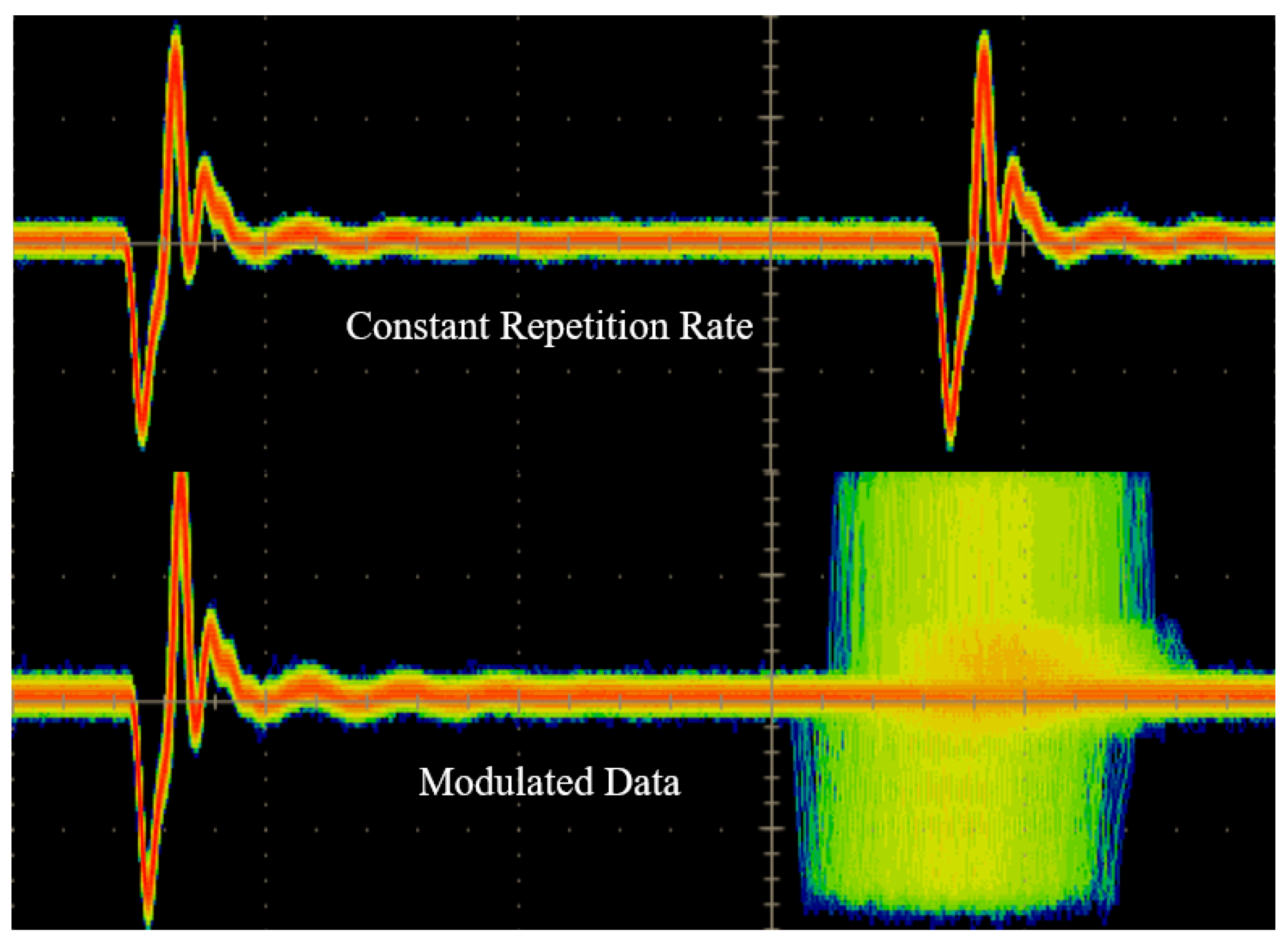
Prior to transmitting the communication string, the FPGA modulator is set to pulse continuously at a repetition rate of 15.625 MHz, which is equivalent to the same symbol being repeated for the selected communication parameters. The pump power and attenuation were used in conjunction to achieve the desired optical power on the receiver by monitoring the PIN on the output. The oscilloscope was used with its fast frame acquisition on the APD signal to determine a starting threshold value for the comparator. A sampling of the fast frame acquisition of the negative signal from the APD differential pair can be seen in Figure 14.
For any given optical power, the reverse bias on the APD and the PGA amplification (from −12 to +52 dB) were tailored to the received optical signal prior to data collection. Due to the APD-integrated transimpedance amplifier (TIA) saturation limits, the reverse bias voltage was limited at high optical powers. For optical powers lower than 2 μ W , the APD reverse bias was pushed as close to breakdown as safely possible to provide the sharpest electrical pulse rising edges. To determine the best PGA gain for the received pulse, the optical power was set to the desired power. Next, the PGA gain was increased from 0 dB until the pulse peak reached about 30 mV on the oscilloscope. Finally, the PGA gains were shifted with the goal of maximizing the separation between the maximum noise amplitude and the minimum pulse amplitude in fast frame measurements. This value was then taken to be the best PGA gain setting for the experiment.
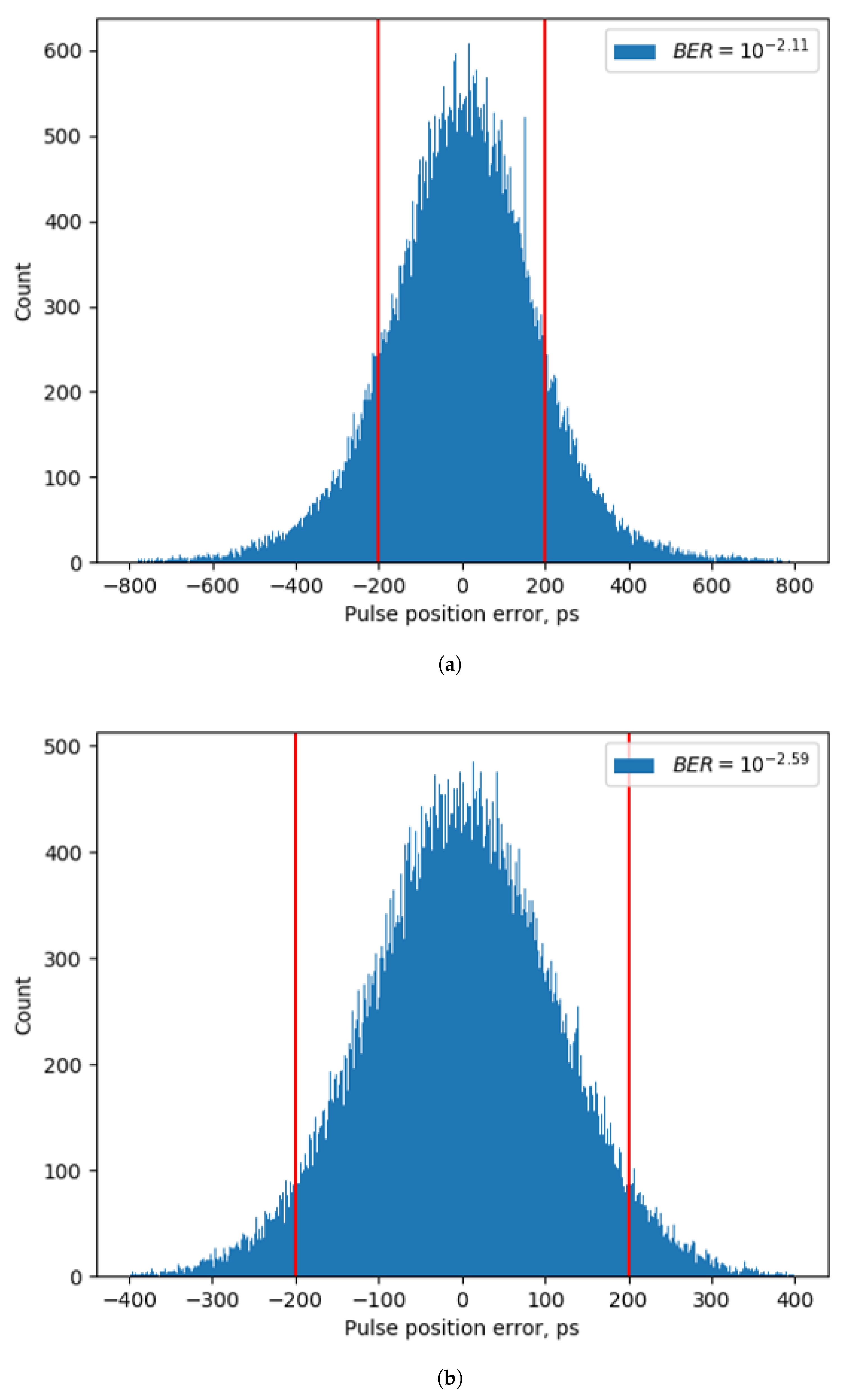
After the optical power and hardware settings were selected, the modulator was switched from sending pulses at a constant repetition rate to repeating a predetermined, pseudorandom data string. This repeated data string generated using the communication parameters in Table 4. Using the starting threshold as a baseline, the peak of the pulse is found by increasing the comparator threshold until the TDC-GPX2 began to have missing time stamps for pulses. The modulated data for three thresholds between the base and the peak of the pulse were measured. This testing was conducted for captured optical signals for peak powers of 102 nW and 176 nW. The time stamp measurements were sent from the TDC-GPX2 development board and stored on a computer to be analyzed.
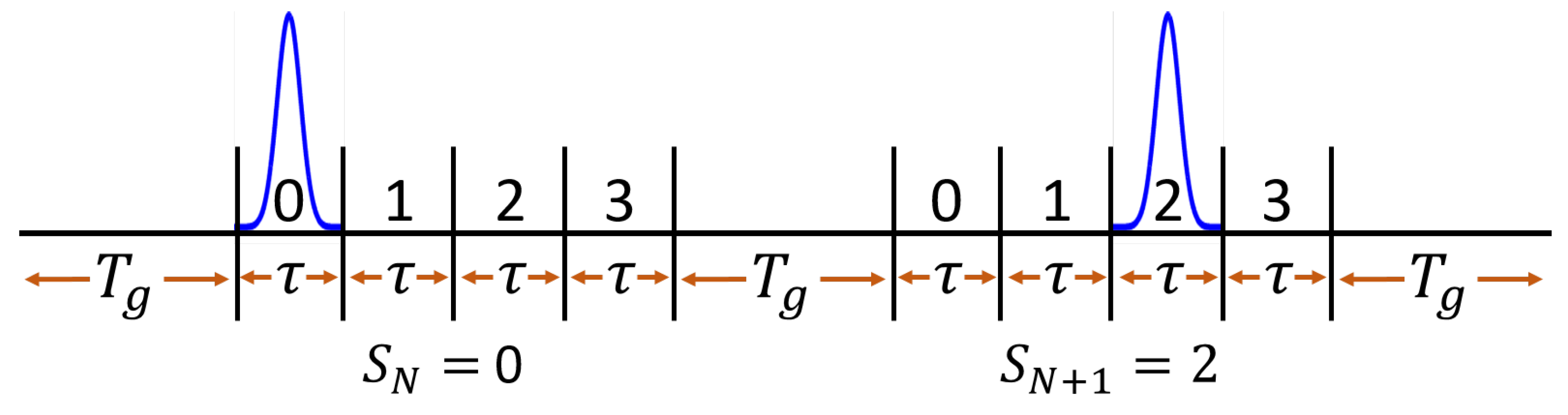
The experiment setup produces data in the form of time stamps, with a resolution of 1 ps and in bursts of 16 consecutive measurements. The majority of the time stamps were acquired by the time-to-digital converter but not recorded because of the limitations of the current TDC interface. The time stamps were encoded in two values, a phase relative to the TDC reference clock with a range of 100 ns called fine time, and a 12 bit clock period counter. Since the reference clock for the TDC oscillates at 10 MHz, the counter saturates and rolls over every 409.6 μ s . In order to reconstruct the data, obtain noise, and obtain the bit error statistics, the data exchanged on the optical link is a 8192-symbol random PPM string. The first step was to correlate a packet with the random string, and find the position of the packet relative to the string. This was done by minimizing the square of the error. For a packet of time stamps t recorded indexed by i, the position p is given by Equation (3):
p = arg min k 1 ; 8192 i t recorded , i t string , ( i + k ) mod 8192 2
Once the data encoded in the packets is known, the time interval between packets can be found. As time moves forward, the TDC clock period counter rolls over, and the string gets repeated, but with a different time period. The counter reaches its maximum every T counter = 409,600 n s and the string period is T string = 524,288 n s . Since the modulator and the TDC share the same clock, the periods for those two events are accurate to the sub-nanosecond level. To find the time interval between packets, Equation (4) is solved for n and m. In Equation (4), p is the packet position from Equation (3), T symbol is the duration of a PPM symbol, S p is the modulated string value for position p, and T slot is the duration of a PPM slot:
m · T string + p · T symbol + S p · T slot n · T counter + t recorded , 1
Equation (4) is solved by successively increasing m and n until both sides match with an acceptable margin of error, within less than 1 n s . The time stamps are now on a common timebase, with no uncertainties due to counter length or string repetition. The Bit Error Ratio (BER) can be estimated by building an histogram of the time errors. The average of the error is removed from histograms, since each set of the acquired data covers several minutes, and a real-time decoder clock recovery mechanism would cancel long term clock slips. For each time stamp, the error from the expected time of the pulse is used to compute the number of errors by symbol. If the error ε is smaller than 1 / 2 · T slot , then there is no error. If ε > 1 / 2 · T slot , but ε < 3 / 2 · T slot , then there is up to 1 bit wrong in the symbol. If ε > 3 / 2 · T slot , but ε < 5 / 2 · T slot , then there is at most 2 bits wrong in the symbol. This was repeated for the number of bits contained in the PPM symbol. The average error over the recorded pulses gives the Bit Error Ratio.

3. Results

3.1. Optical Amplifier Characterization Results

The measured peak power from the FLAT (data markers) can be seen in Figure 15. These values are adjusted for the added attenuation, but include the 31.7% losses from output fiber optics. The pump power shown in Figure 15 are pump powers at the entrance of the erbium doped fiber from the pump pickoff measurements. The seed peak power was ∼4.7 mW and the seed pulse width was ∼2.5 ns. When comparing the seed pickoff PIN with the amplifier output PIN at similar signal amplitudes, some measurements experienced a pulse width increase <10% while others had a negligible increase. In Figure 15, the 26 cm fiber appears to be approaching gain saturation at the 300 mW pump. The 55 cm fiber has two steps in the data, at around 75 mW and 225 mW, since this is where the attenuation was changed out during a fiber characterization and there was likely some variation in the attenuation from dust or particles. A similar attenuation step can be seen in the 86 cm and 106 cm fibers around 200 mW. Additionally, it can be seen in Figure 15 that the required threshold pump power to overcome signal absorption when the output peak power is greater than zero increases with increasing fiber length. The 55 cm fiber had the highest peak power at 300 mW pump power and the other three fibers had peak powers of approximately the same magnitude to each other, but less than the 55 cm fiber. If all fibers were identical except for length and if sufficiently high pump power was available at the erbium fiber entrance, the 86 cm and 106 cm fibers would have produced greater peak powers than the 55 cm fiber.
The results from the dynamic simulation for a 26 cm, 55 cm, 86 cm, and 106 cm fiber (curves) can be seen in Figure 15. The pump power for each fiber was evaluated between 0 and 300 mW at the entrance of the erbium doped fiber. The seed laser pulse width and peak power used in each fiber simulation corresponded to the mean pulse width and peak power measured for each fiber during the FLAT characterization experiment. The seed peak powers were all selected to be ∼4.7 mW and the seed pulse widths were all selected to be ∼2.5 ns. The parameters that were iterated for each fiber separately to match the measured FLAT outputs can be found in Table 5. No value of C u p c o n was specified for this fiber, but it was predicted that the C u p c o n in all fibers would be close to one another. The reasoning for this assumption is that fibers of the same product model are likely to have the same manufacturing process, and thus should exhibit similar ion-to-ion interactions. The losses were a set of variables that could differ for all fibers, since the loss depends on how well light is coupled at the connectors. Variables that affect these connector losses include how well the fiber cores align, fiber geometric irregularities, and the finish quality of the connector. All of these variables can be different from fiber to fiber and can be difficult to characterize beforehand.
The measured steady state peak power and the simulated steady state peak power match well for the two shorter fibers as seen in Figure 15, except for step in data for the 55 cm fiber. The two longer fibers do not closely match until after 200 mW of pump power.
The MOCT EDFA simulated peak power as a function of guard time for a variety of supplied pump powers can be seen in Figure 16. There are diminishing returns in produced peak power for increasing guard time and pump power. For the simulation in Figure 16, a single 4 W pump is sufficient to close all three links. It should be noted that a 0.5 W pump power, with a guard time of 50 ns is predicted to produce amplified pulses with a peak power of 1.077 W.

3.2. Benchtop Transceiver Testing Results

After accounting for the losses after the erbium doped fiber exit and added attenuation in the U-bench, the amplifier produced 2.5 ns wide pulses with a peak power of 2.13 W during the amplifier verification testing. When adjusting for a 35.7% loss, which was present in the optical amplifier characterization simulation, the peak power was 1.37 W. The ND filter used for attenuation in the U-bench has a 5% uncertainty and the monitor diode on the pump laser has approximately a 10% uncertainty.
The BER measurement experiment results can be seen in Table 6. In this test, the higher optical power (176 nW) cases had a lower BER than the 102 nW cases. Histograms at the best thresholds for each optical power can be seen in Figure 17. The best threshold for the 102 nW case (Figure 17a) was determined to be 20 mV and the best threshold for the 176 nW case (Figure 17b) was determined to be 28 mV.

4. Discussion

4.1. Optical Amplifier Characterization Discussion

In Figure 15, all four simulations agreed well with the measured data. The best fits were with the 26 and 55 cm fibers, except for the attenuation step between 66 mW and 226 mW of pump power. For these pump powers on the 55 cm fiber, it is believed there was additional attenuation than nominal, such as dust or other particles on the ND filter that were not fully accounted for when adjusting the attenuated measured signal. The 86 cm and 106 cm fibers did not appear to be matched as well, but this is also believed to be from an attenuation step. The 86 cm fiber had a change in attenuation at 191 mW of pump power and the 106 cm fiber had an attenuation change at a pump power of 208 mW, which both correspond to the steps in data. Initially, the fit parameter values in Table 5 were all similar; however, the 86 cm fiber and the 106 cm fiber fit much better by almost doubling C u p c o n and increasing the connector losses by ∼25% each. This was believed to be caused by either differences in the manufacturing batch or connector polishing, since the 86 cm and the 106 cm fiber were purchased a few years after the 26 cm and 55 cm fibers. Additionally, it is possible that the model does not fully capture some losses that increase with fiber length and is thus negligible for the 55 cm and 26 cm fibers and not not negligible for 86 cm and 106 cm. One possibility is that the ASE spectrum may be too narrow or the steps may be too coarse to capture the losses. The ASE band simulated was 1520 to 1580 nm, since this is the optical band that can pass through the exit isolator and are included in the detector measurement.
The model could be better evaluated if measurements at higher pump powers were taken. The reason for the 300 mW cap of pump power with a pump capable of delivering 500 mW of power is that the losses from the pump to the entrance of the erbium doped fiber were high (∼40%). These losses were attributable to the addition of the pump pickoff measurements that were used to provide a higher certainty of the pump power emitted than the integrated monitor diode. The pump pickoff utilized HI1060FLEX fiber which has different optical properties than the SMF-28 fiber that was used throughout the rest of the fiber optics. It should be noted that the erbium doped fiber was not SMF-28 but is designed to be compatible with it. Splicing all connections, utilizing the same fiber (or compatible), and having a well-calibrated pump monitor diode would increase the pump power delivered to the erbium doped fiber without sacrificing knowledge of how much pump power is being emitted.
As seen in the simulation results in Figure 16, the MOCT amplifier design is anticipated to be able to close all three optical links. Both the guard time and the pump power should be considered when tuning the transmitted peak power for an optical link. For instance, consider a LEO to LEO crosslink where M is 32 and the slot width is 400 ps. Utilizing 1.5 W of pump power requires ∼15 μ s guard time and the corresponding data rate is ∼333 kbps. Increasing the pump to 4 W requires a guard time of ∼2 μ s and the data rate for this higher pump power goes up to ∼2.48 Mbps. Depending on the mission situation, it may be worth the additional power consumption to achieve a higher data rate.

4.2. Benchtop Transceiver Testing Discussion

The amplifier characterization simulation shows a simulated amplifier design that can close all three of the optical link scenarios. The amplifier verification test was conducted to demonstrate that the amplifier design is able to achieve the expected performance at low pump powers. While the repetition rate was lower, the seed peak was lower, and the pulse width was wider for the hardware demonstration than the MOCT simulation, the optical amplifier test had ∼21.4% higher peak power than the simulation. Higher repetition rates are associated with shorter guard times, so it is expected that the amplifier demonstration (51.2 ns guard time) would have a higher peak power than the simulation (50 ns guard time) if all other variables were the same. For a fixed pulse energy in an unsaturated amplifier, wider pulses are expected to yield lower peak powers, which did not seem to significantly impact transmit peak power here. Additional simulations and tests should be conducted in order to better verify the amplifier’s performance, investigate the seed laser influence on performance, and update the model where necessary to predict performance. The amplifier verification test did show that this design is able to transmit pulses with a peak power on the order of a Watt. This amplifier is in a single, backwards pumping configuration and as the pump and transmitted peak powers increase in future tests, it may be determined that a more complicated configuration is required.
The BER measurement test was conducted in order to evaluate the link performance when the detector receives an optical power that is expected during a communication. The link budget assumes that 100 nW is required for the APD to detect a pulse, so the BER was measured at 102 nW and 176 nW to see how increasing the power received influences BER. Increasing the optical power from 102 nW to 176 nW decreased the BER by about a factor of 3. It should be noted that the indicated powers were determined as the maximum power that could be captured by the APD, so better focusing the lens onto the APD or improving the alignment could increase the actual power seen by the APD. The BER could also be reduced by increasing slot width at the cost of lowering the data rate. Even if there are bit errors during communication on a mission, error correction codes can be implemented to help reduce bit errors. Further investigation will need to be conducted to sweep more optical powers, thresholds, and communication parameters to better determine what is the lowest BER MOCT can achieve and under what conditions.

5. Conclusions

The MOCT lasercom system aims to provide power efficient, pulsed optical communication to nanosatellite platforms at lunar distances. The amplifier design is expected to be able to close optical links from LEO to Earth, LEO to LEO, and Moon to Earth based upon the simulation used to model the amplifier design. This simulation predicts that the amplifier design, utilizing 4 W of pump power, will produce optical pulses with a peak power of ∼1 kW. The amplifier verification test showed that hardware in the MOCT design configuration, utilizing 500 mW of pump power, is able to produce amplified pulses with a peak power of 1.37 W. This demonstrated peak power of 1.37 W is 20% higher than the simulated results, which had different seed laser parameters and a marginally higher pulse repetition rate. The BER measurement demonstrated core functionality of the majority of the MOCT components and gave insight on the expected communication performance, where the measured BER was 0.776% for 102 nW of peak power and 0.257% for 176 nW of peak power.

Author Contributions

Conceptualization, J.W.C. and P.S.; Methodology, N.B., M.C., and P.S.; Software, N.B., M.C., T.R., and P.S.; Validation, N.B.; Formal Analysis, P.S.; Investigation, N.B., M.C., T.R., and P.S.; Resources, N.B., J.W.C., M.C., S.P., T.R., and P.S.; Data Curation, N.B. and P.S.; Writing—Original Draft Preparation, N.B., M.C., S.P., T.R., and P.S.; Writing—Review and Editing, N.B., J.W.C., M.C., S.P., T.R., and P.S.; Visualization, N.B., M.C., T.R., S.P. and P.S.; Supervision, N.B. and J.W.C.; Project Administration, N.B. and J.W.C.; Funding Acquisition, J.W.C.

Funding

This research was funded by the National Aeronautics and Space Administration Early Career Faculty Program Grant No. NNX14AO53G and the National Aeronautics and Space Administration Cooperative Agreement No. NNX16AT13A.

Acknowledgments

The authors would like to acknowledge Daniel Raible from NASA Glen Research Center for his support in the initial stages of development of the Miniature Optical Communication Transceiver.

Conflicts of Interest

The authors declare no conflict of interest.

Abbreviations

The following abbreviations are used in this manuscript:
ASEAmplified Spontaneous Emission
APDAvalanche Photodetector
BERBit Error Ratio
CSACChip Scale Atomic Clock
CWContinuous Wave
DLLDelay Locked Loop
EDFA Erbium Doped Fiber Amplifier
FETField-Effect Transistor
FLASHEFast Laser Advanced Switching High-Frequency Emitter
FLATFiber Laser Amplifier Testbed
FPGA Field Programmable Gate Array
FWMFour-Wave Mixing
HUCHomogeneous Upconversion
LADEELunar Atmosphere And Dust Environment Explorer
LEOLow Earth Orbit
LLCDLunar Laser Communication Demonstration
LVDSLow-Voltage Differential Signaling
MOCTMiniature Optical Communication Transceiver
MOPFA Master Oscillator Power Fiber Amplifier
NASA National Aeronautics and Space Administration
NDNeutral-Density
PCBPrinted Circuit Board
PGA Programmable Gain Amplifier
PIQPair-Induced Quenching
PLLPhase Locked Loop
PPMPulse Position Modulation
PSSLPrecision Space Systems Laboratory
SBSStimulated Brillouin Scattering
SDPMSoftware Defined Pulse Modulator
SERDESSerializer/Deserializer
SMASubMiniature version A
SPISerial Peripheral Interface
SRSStimulated Raman Scattering
SWaPSize, Weight, and Power
TDCTime-to-Digital Converter
TECThermoelectric Cooler
TIA Transimpedance Amplifier
WDMWave Division Multiplexer

Appendix A

Appendix A.1. Optical Link Parameters, Terms, and Equations

Table A1. The link parameters, or inputs, for the link budget that are used to predict how much of the transmitted optical signal is captured by the receiver.
Link ParameterDescription
λ wavelength
w 0 beam waist
zlink distance
ϕ total beam half angle divergence
rradial offset of receiver from beam center
w ( z ) 1 / e 2 beam radius at distance z
r r x receiver radius
U t x transmitter pointing uncertainty
U r x receiver pointing uncertainty
G t x = 4 / ϕ 2
G r x = ( 2 π r r x / λ ) 2
L r a n g e = ( λ / ( 4 π z ) ) 2
T p o i n t = 2 · e 2 · U t x 2 / ϕ 2
R p o i n t = cos U r x
G [ d B ] = 10 · l o g 10 ( G )
Table A2. The link terms are used to describe the communication link and are combined to determine how much of the transmitted power is captured by the receiver.
Link TermDescription
P r x received power
P t x transmitted power
G t x transmitter gain
G r x receiver gain
L r a n g e range loss
η t x transmitter optical efficiency
η a t m atmospheric transmission efficiency
η r x receiver optical efficiency
T p o i n t transmitter pointing gain
R p o i n t receiver pointing loss
Table A3. Link terms values used for the three optical link scenarios for MOCT. All values are in decibels.
Link G tx G rx L range η tx η atm η rx T point R point
Moon-Earth93.20126.14−309.77−3.25−0.59−3.250.350
LEO–Earth83.57106.14−252.16−3.25−0.59−3.252.720
LEO–LEO83.5786.14−258.18−3.250−3.252.720

References

  1. Boroson, D.M.; Robinson, B.S.; Murphy, D.V.; Burianek, D.A.; Khatri, F.; Kovalik, J.M.; Sodnik, Z.; Cornwell, D.M. Overview and results of the Lunar Laser Communication Demonstration. SPIE LASE 2014, 8971, 8971. [Google Scholar] [CrossRef]
  2. LADEE (Lunar Atmosphere and Dust Environment Explorer). Available online: https://earth.esa.int/web/eoportal/satellite-missions/l/ladee (accessed on 16 February 2018).
  3. Chen, W.; Sun, J.; Hou, X.; Zhu, R.; Hou, P.; Yang, Y.; Gao, M.; Lei, L.; Xie, K.; Huang, M.; et al. 5.12 Gbps optical communication link between LEO satellite and ground station. In Proceedings of the 2017 IEEE International Conference on Space Optical Systems and Applications (ICSOS), Naha, Japan, 14–16 November 2017; pp. 260–263. [Google Scholar]
  4. Liao, S.K.; Cai, W.Q.; Liu, W.Y.; Zhang, L.; Li, Y.; Ren, J.G.; Yin, J.; Shen, Q.; Cao, Y.; Li, Z.P.; et al. Satellite-to-ground quantum key distribution. Nature 2017, 549, 43. [Google Scholar] [CrossRef] [PubMed]
  5. Hemmati, H. Deep Space Optical Communications; Deep Space Communications and Navigation Systems Center of Excellence, Jet Propulsion Laboratory, California Institute of Technology: Pasadena, CA, USA, 2005; Volume 11. [Google Scholar]
  6. Barnwell, N. Free-Space Optical Links for Small Spacecraft Navigation, Timing, and Communication. Ph.D. Thesis, University of Florida, Gainesville, FL, USA, 2018. [Google Scholar]
  7. Li, J.; Hylton, A.; Budinger, J.; Nappier, J.; Downey, J.; Raible, D. Dual-pulse pulse position modulation (DPPM) for deep-space optical communications: Performance and practicality analysis. In Proceedings of the 2012 International Conference on Wireless Communications and Signal Processing (WCSP), Huangshan, China, 25–27 October 2012; pp. 1–7. [Google Scholar]
  8. Microsemi Corporation. DS0128 Datasheet IGLOO2 FPGA and SmartFusion2 SoC FPGA; Rev. 11; Microsemi Corporation: Aliso Viejo, CA, USA, 2017. [Google Scholar]
  9. Microsemi Corporation. CSAC SA.45s Datasheet; Rev. C; Microsemi Corporation: Aliso Viejo, CA, USA, 2018. [Google Scholar]
  10. nLIGHT, Inc. Liekki Er80-8/125—Large Mode Area Erbium Doped Fiber; nLIGHT, Inc.: Vancouver, WA, USA, 2017. [Google Scholar]
  11. AMS AG. TDC-GPX2 4-Channel Time-to-Digital Converter Datasheet; v1-03; AMS AG: Premstaetten, Austria, 2017. [Google Scholar]
  12. Serra, P. Integrated, Low-Power Sub-Nanosecond Timing Systems for Space Navigation and Communication. Ph.D. Thesis, University of Florida, Gainesville, FL, USA, 2018. [Google Scholar]
  13. Lau, K.Y. Gain switching of semiconductor injection lasers. Appl. Phys. Lett. 1988, 52, 257–259. [Google Scholar] [CrossRef]
  14. Paschotta, R. RP Fiber Power—Simulation and Design Software fore Fiber Optics, Amplifiers and Fiber Lasers. Available online: https://www.rp-photonics.com/fiberpower.html (accessed on 6 June 2018).
  15. Novotny, S. nLIGHT Sales and Application Engineer; Email Conversation; nLIGHT, Inc.: Vancouver, WA, USA, May 2018. [Google Scholar]
Figure 1. Example string of pulse position modulation (PPM) where the first symbol transmitted (S N ) encodes a “0” and the second symbol (S N + 1 ) encodes a “2”.
Aerospace 06 00002 g001
Figure 2. MOCT architecture.
Aerospace 06 00002 g002
Figure 3. Here is the FPGA based modulator for MOCT on its development board. It is responsible for sending data to the seed laser in order to be transmitted to the receiver.
Aerospace 06 00002 g003
Figure 4. Seed laser pulse driver circuit.
Aerospace 06 00002 g004
Figure 5. (A) 100 ps pulses aligned to the reference clock, 200 ps per division; (B) 100 ps pulses self-triggered, 100 ps per division [12].
Aerospace 06 00002 g005
Figure 6. FLASHE 1.0 current driver module with 1531 nm laser for in-lab experiments.
Aerospace 06 00002 g006
Figure 7. The FLAT benchtop optical amplifier setup at the University of Florida in a forward pumping configuration. The FLAT was used to characterize the transmitter hardware for MOCT.
Aerospace 06 00002 g007
Figure 8. EDFA pumping configurations.
Aerospace 06 00002 g008
Figure 9. The left picture shows the NOVA receiver board used in laboratory testing. The center picture is the NOVA receiver board inside of its housing for both thermal dissipation and positioning of the focusing lens. The right photo is looking at the active element through the focusing lens which increased the APD effective active area size from 200 μ m to ∼5 mm. The focusing lens was aligned to this magnification (∼25×) in order to have an effective active area larger than the 3.6 mm collimated amplifier output signal and maintain low laboratory alignment requirements.
Aerospace 06 00002 g009
Figure 10. The TDC-GPX2 evaluation board used for laboratory testing of MOCT. The added SMA cables and resistors enable LVDS inputs for this development board.
Aerospace 06 00002 g010
Figure 11. The setup used for characterizing the FLAT. The optics before the entrance and after the exit of the erbium doped fiber were kept the same except the free-space attenuation on the U-bench. The erbium doped fiber was swapped out after a series of measurements at different pump power were made.
Aerospace 06 00002 g011
Figure 12. Block diagram of the end-to-end MOCT benchtop transceiver testing setup. Both of the PIN diodes and the APD are also monitored by an oscilloscope. The TDC is connected to a computer via USB cable. The orange lines are optical signals and the black arrows are electrical connections.
Aerospace 06 00002 g012
Figure 13. Photo of the end-to-end MOCT benchtop transceiver testing setup.
Aerospace 06 00002 g013
Figure 14. The oscilloscope reading is shown for the negative APD output signal. Two fast frame measurements are shown to visualize the difference between a non-modulated signal and a modulated signal. On the modulated fast frame capture, 2000 frames are shown within the single image and triggered off of a random pulse within the transmitted data. This shows the range of relative pulse positions for the data string.
Aerospace 06 00002 g014
Figure 15. The measured steady state peak power plotted with the simulated steady state peak power, using parameter values in Table 5, with four fiber lengths: 26 cm, 55 cm, 86 cm, and 106 cm. The data markers are the experimental measurements from the FLAT characterization experiment while the curves are from the simulation.
Aerospace 06 00002 g015
Figure 16. The simulated transmitted peak power for the MOCT EDFA design. The transmitted peak power is shown as a function of guard time for a few select pump optical powers: 0.5 W, 1 W, 1.5 W, 2 W, 3 W, and 4 W. A pump power of 5 W is also included for comparison. A transmitter optics loss of 35.7% was accounted for in this simulation. The required transmitted optical power to close the LEO–LEO, LEO–Earth, and Moon-Earth with 3 dB margin is also shown.
Aerospace 06 00002 g016
Figure 17. (a) pulses with 102 nW peak power captured and 20 mV threshold; (b) pulses with 176 nW peak power captured and 28 mV threshold. Histograms of the time stamps and pulse position error at the best thresholds for 102 nW and 176 nW. A slot width of 400 ps is shown on each histogram with vertical red lines, where time stamps located outside these lines are bit errors.
Aerospace 06 00002 g017
Table 1. The required peak powers for the MOCT link scenarios for select transmitter (Tx) and receiver (Rx) diameters.
SenarioLink Dist.Tx Diam.Rx Diam.Req. Peak Power
Moon to Earth 3.8 × 10 5 km10 cm1 m1.0 kW
LEO Crosslink1000 km1 cm1 cm340 W
LEO to Earth500 km1 cm10 cm1.0 W
Table 2. The experimental parameters used for characterizing the FLAT.
ParameterValue
Repetition Rate20 MHz
Seed Peak Power at Entrance4.7 mW
Seed Pulse Width2.5 ns
Fiber Lengths26, 55, 86, 106 cm
Pump Power at Entrance0–300 mW
Table 3. Simulation parameters used for all fibers in the FLAT simulation.
ParameterValue
seed wavelength1531 nm
pump wavelength976 nm
ASE spectrum1520 nm to 1580 nm
fiber core diameter7.6 μ m
doping concentration 37 × 10 24 ions/m 3
cluster size2 ions/cluster
fraction of ions in clusters 14 %
homogeneous conversion type2 ion interaction
seed input loss 4 %
pump input loss 4 %
signal output loss 35.7 %
pump output loss 99.9 %
Table 4. Optical communication parameter set that was investigated. The guard time was selected to close the LEO to Earth optical link. The corresponding raw data rate was calculated from Equation (2).
Pulse WidthNum. Slots, MGuard TimeSlot WidthRaw Data Rate
2.5 ns3251.2 ns400 ps78.1 Mbps
Table 5. Simulation parameters used for all fibers in the FLAT simulation.
Fiber Len. C upcon Extra Pump LossExtra Seed LossExtra Output Loss
26 cm 2.44 × 10 23 1 % 1 % 1 %
55 cm 2.44 × 10 23 4 % 4 % 4 %
86 cm 4.36 × 10 23 27 % 27 % 27 %
106 cm 4.36 × 10 23 25 % 25 % 25 %
Table 6. Measured BER for the optical communication parameter set investigated.
Optical Peak PowerThresholdBERBER (%)
102 nW20 mV 10 2.11 0.776%
102 nW23 mV 10 2.11 0.776%
102 nW25 mW 10 2.07 0.851%
176 nW20 mV 10 2.47 0.339%
176 nW28 mV 10 2.59 0.257%
176 nW35 mW 10 2.52 0.302%

