A Review and Comparison of Solid, Multi-Strands and Litz Style PCB Winding


Abstract
:
1. Introduction
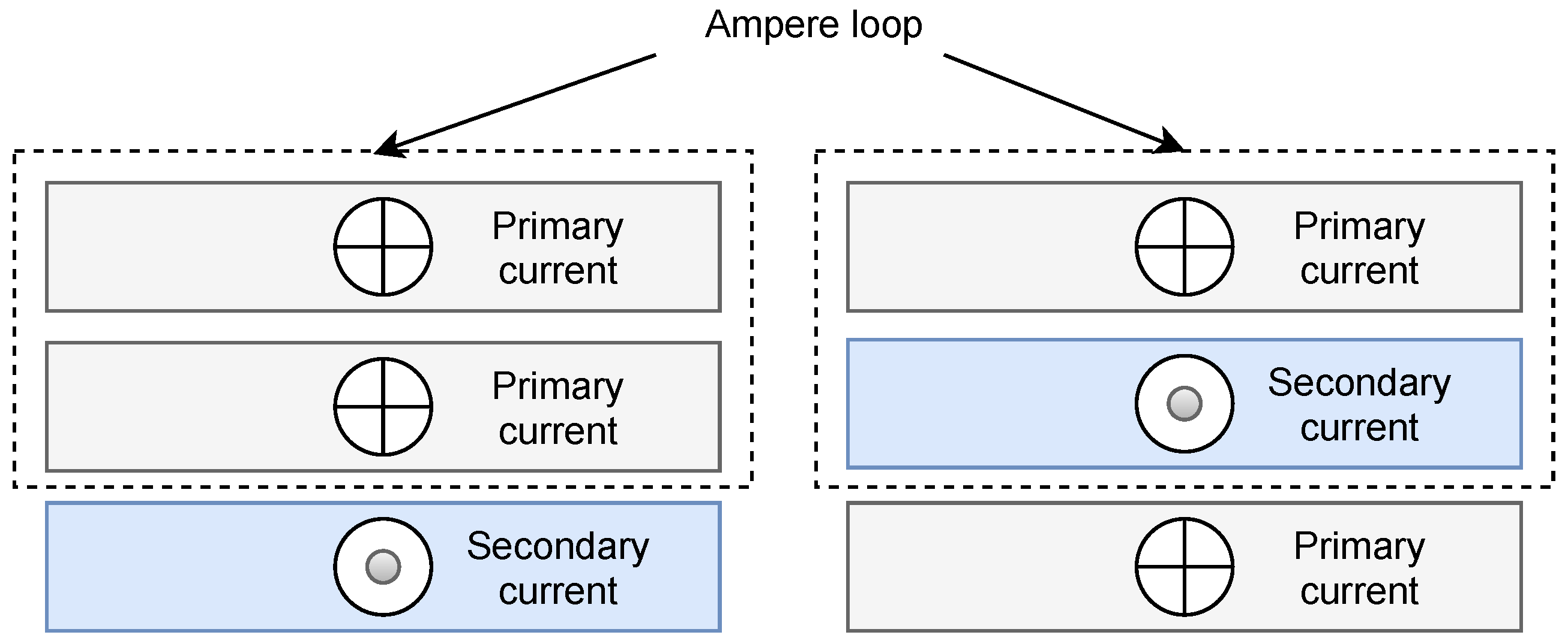
1.1. Interleaving Windings to Reduce AC Resistance
1.2. Optimizing AC Resistance by Changing Winding Dimensions
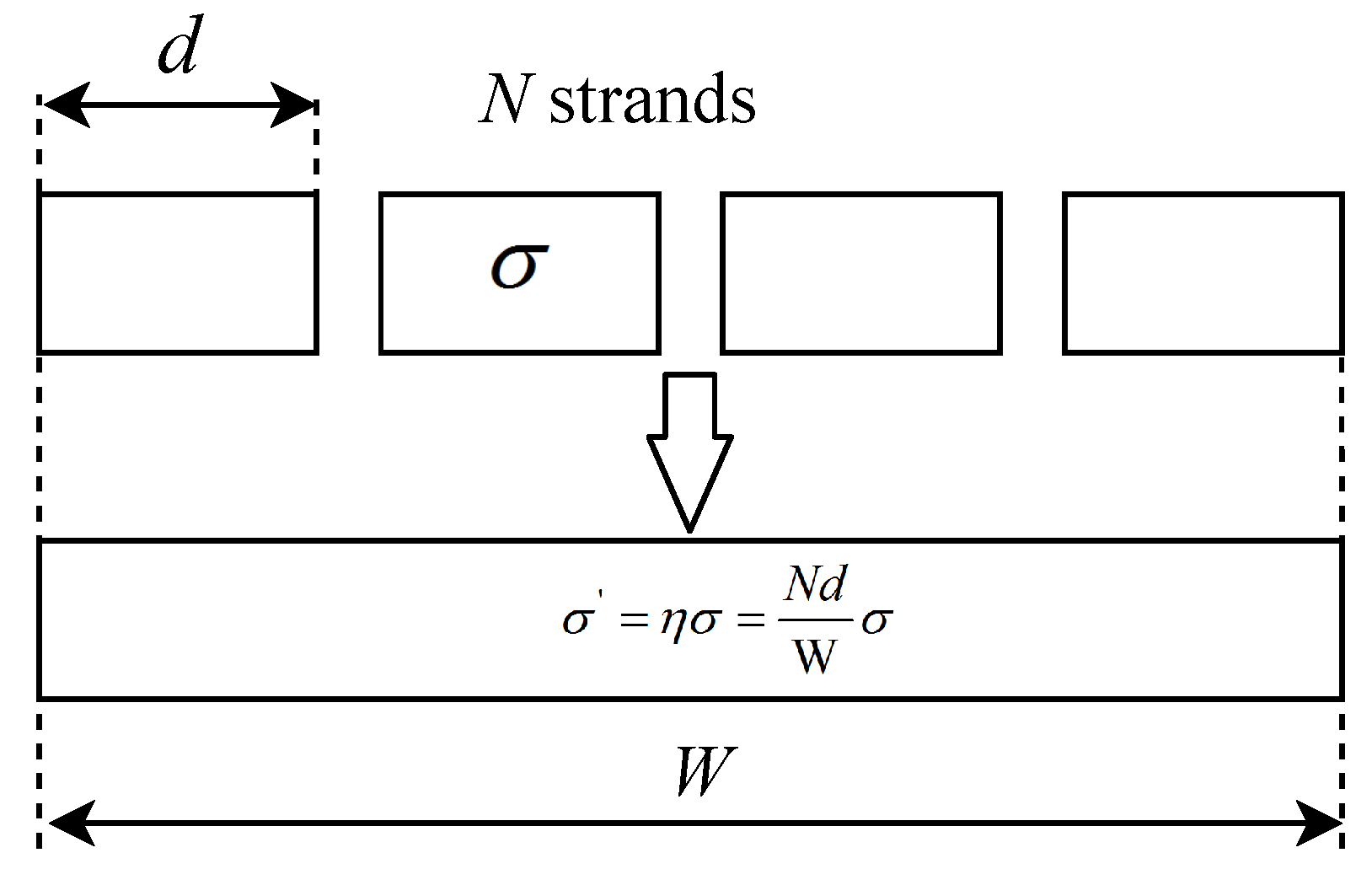
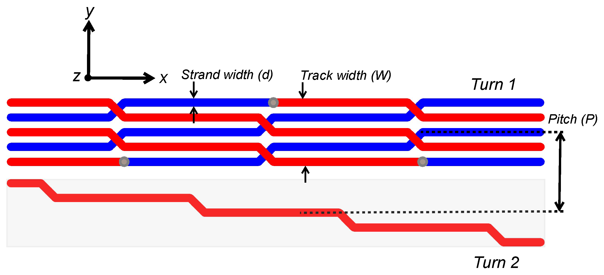
1.3. Using Multi-Strands and Litz Style PCB Windings to Reduce Skin and Proximity Effect
2. Performance Evaluation
2.1. Solid Two Layers Winding Modeling
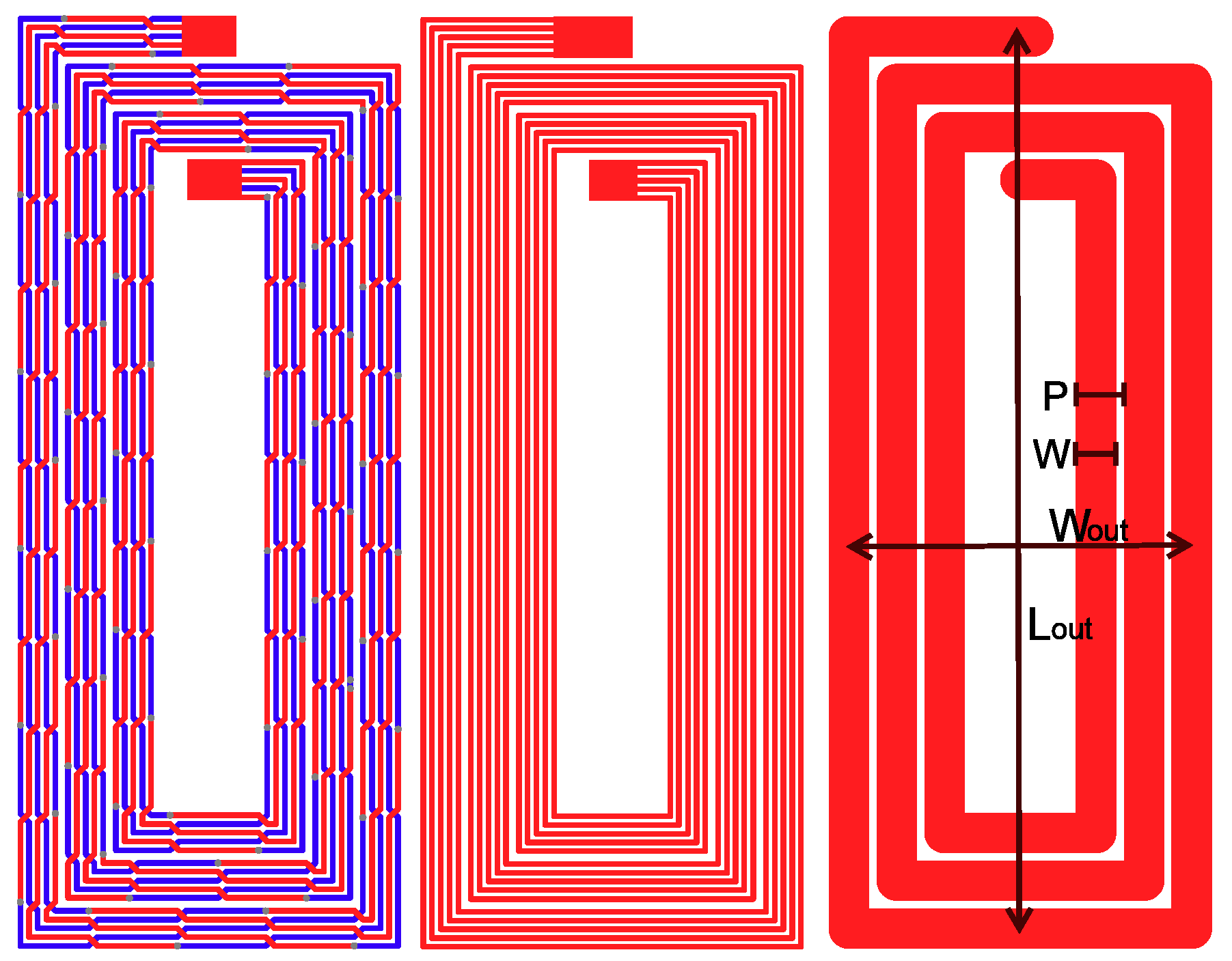
2.2. Two-Layer Multi-Strands Winding
2.3. Litz Style PCB Winding
2.4. Performance Comparison
- -
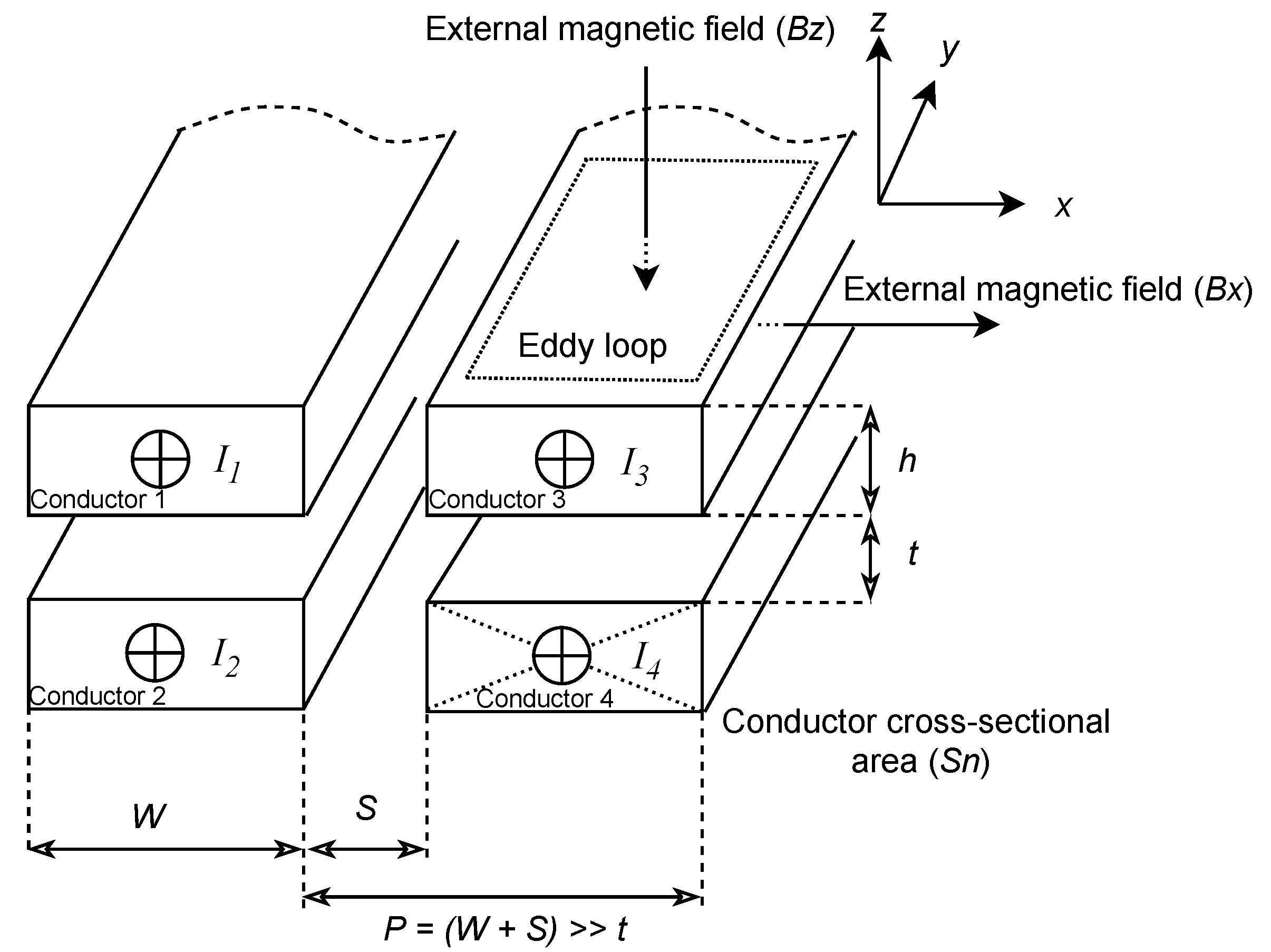
- The track pitch (P) is many times larger than PCB thickness (h) and the redistribution of current density in each track at high frequency does not affect on its external fields.
- -
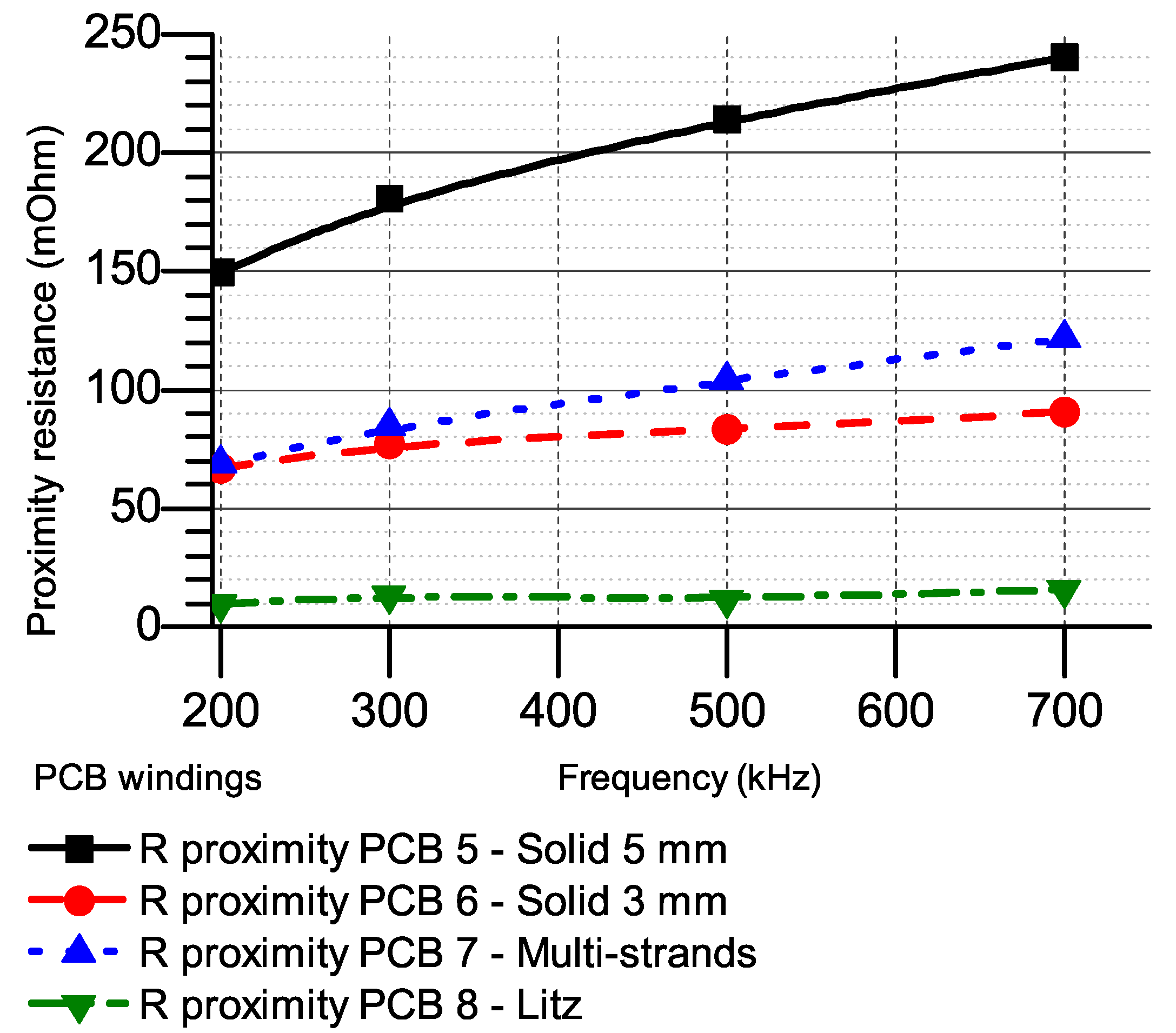
- The Litz style winding is considered to completely remove proximity resistance.
- -
- The skin ratio () is considered to have a slight change while changing the track width [14].
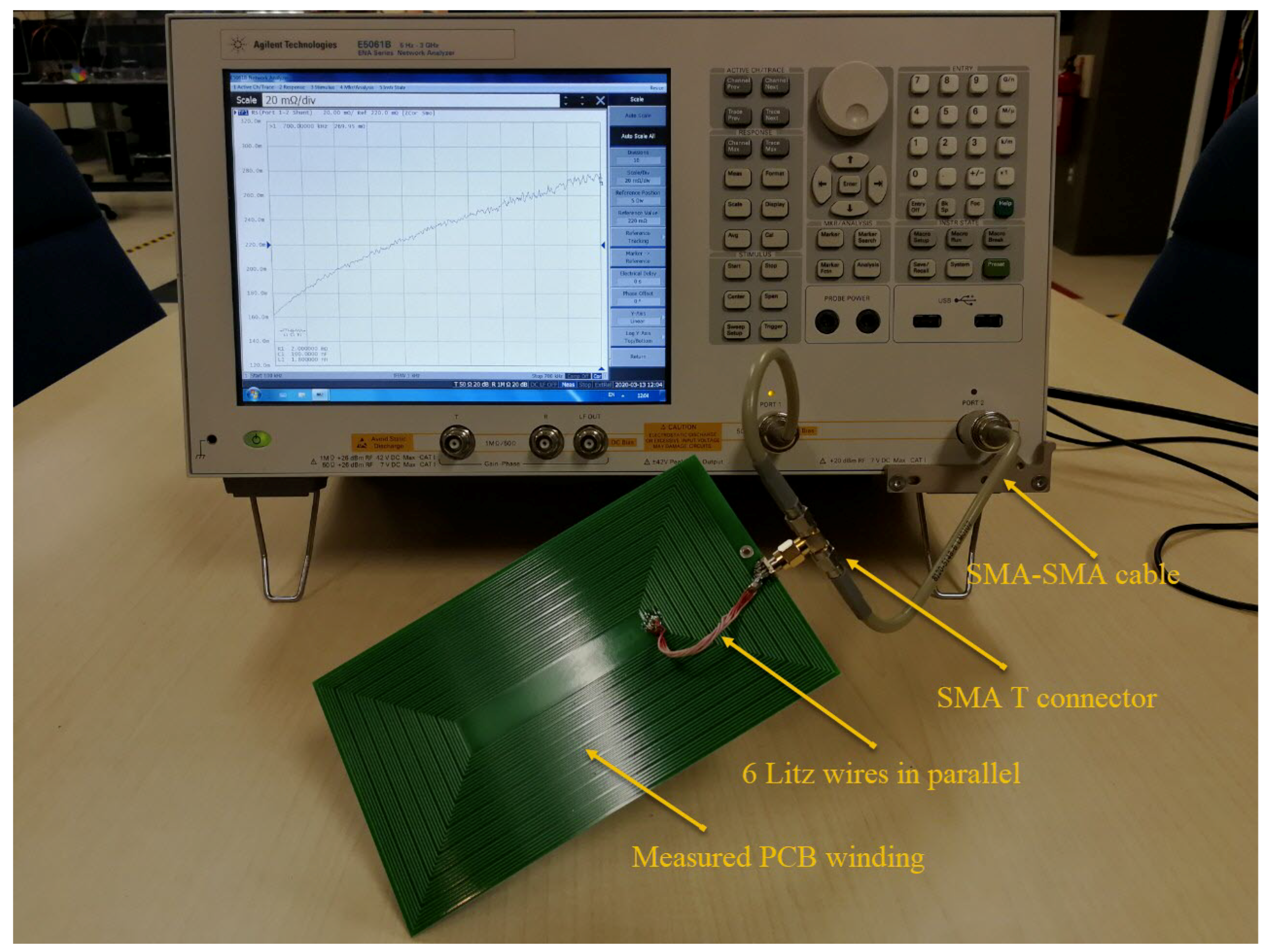
3. Simulation and Measurement Results
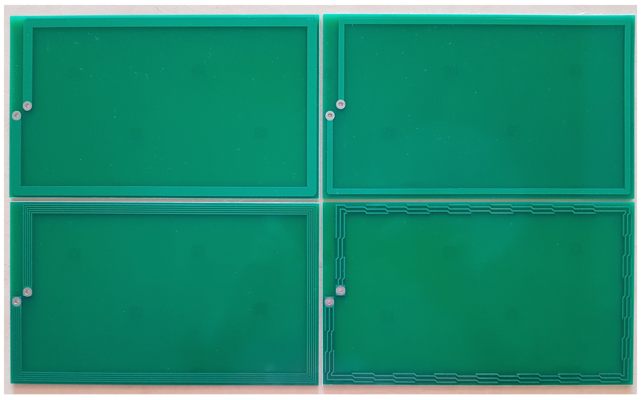
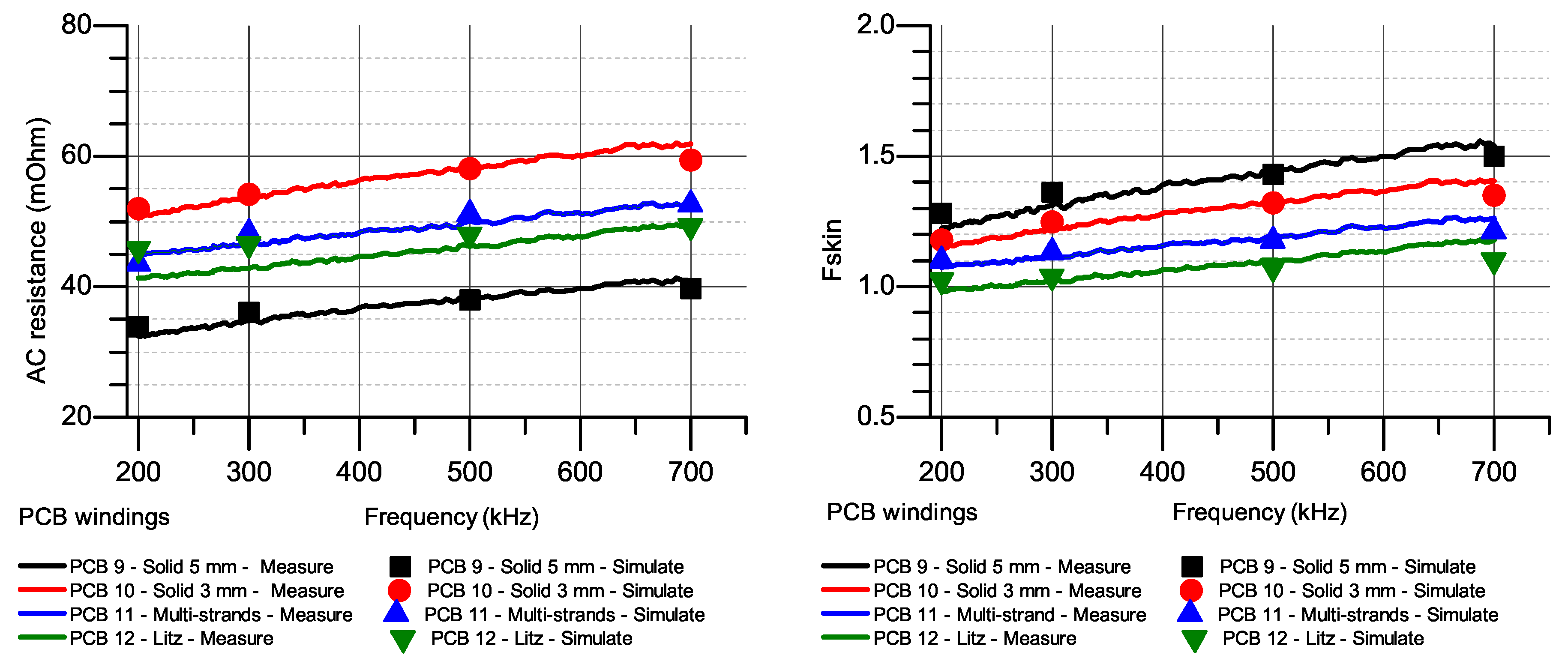
3.1. Case Study 1: 1-Turn 1-Layer PCB Windings
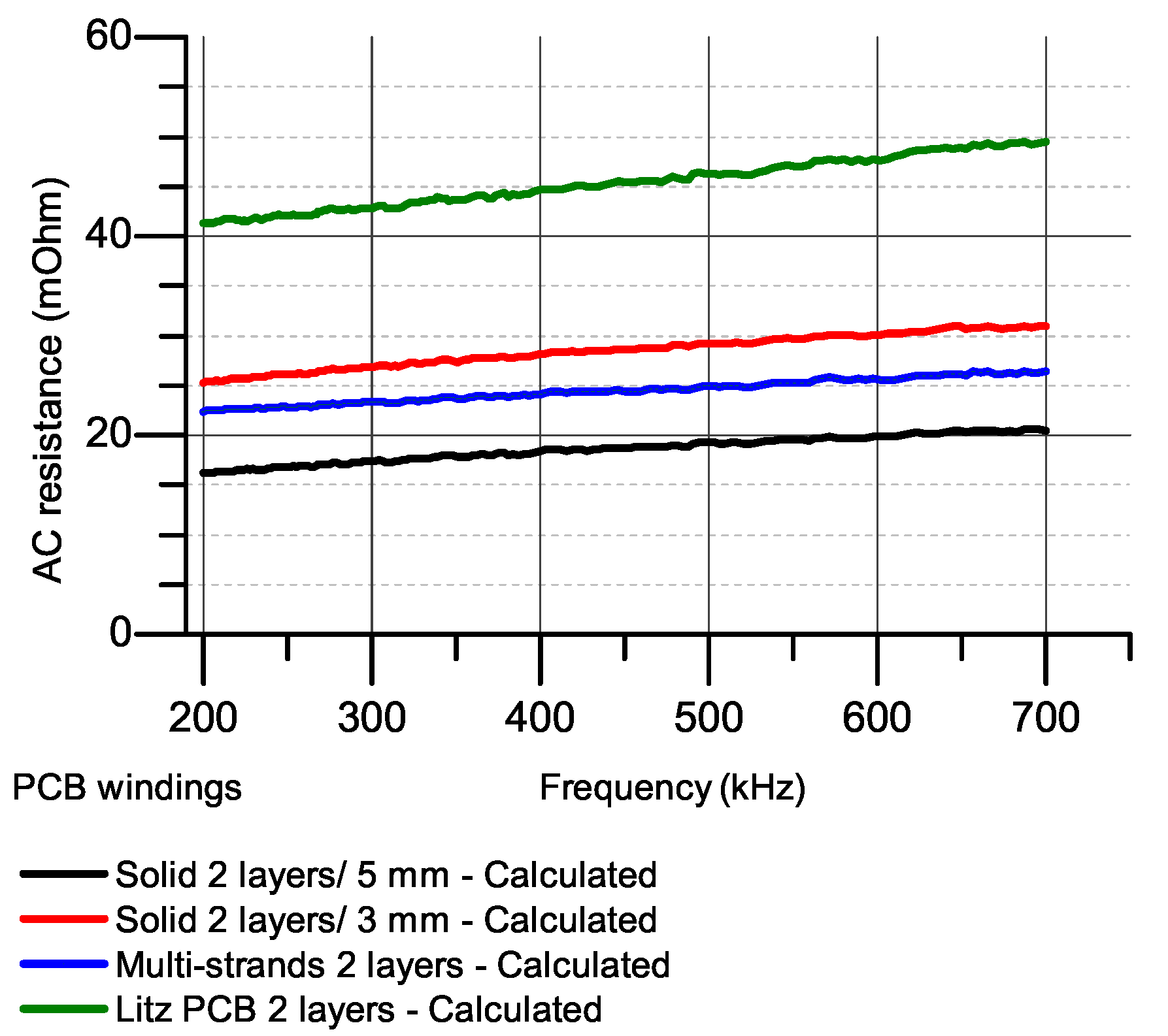
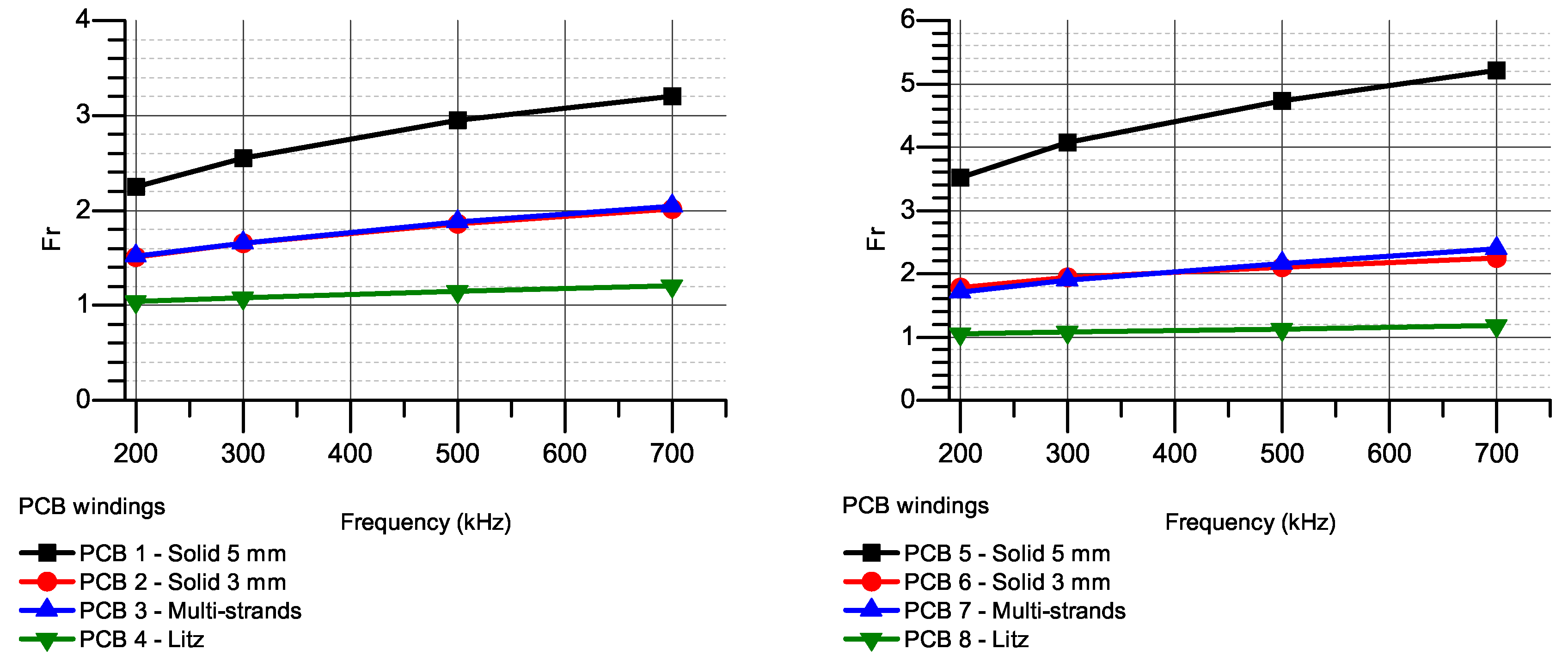
3.2. Case Study 2: 3-Turn 2-Layer PCB Windings
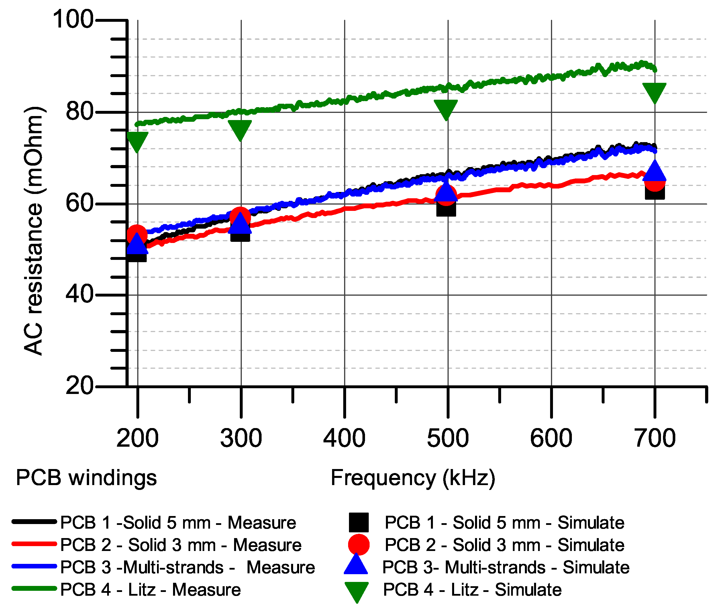
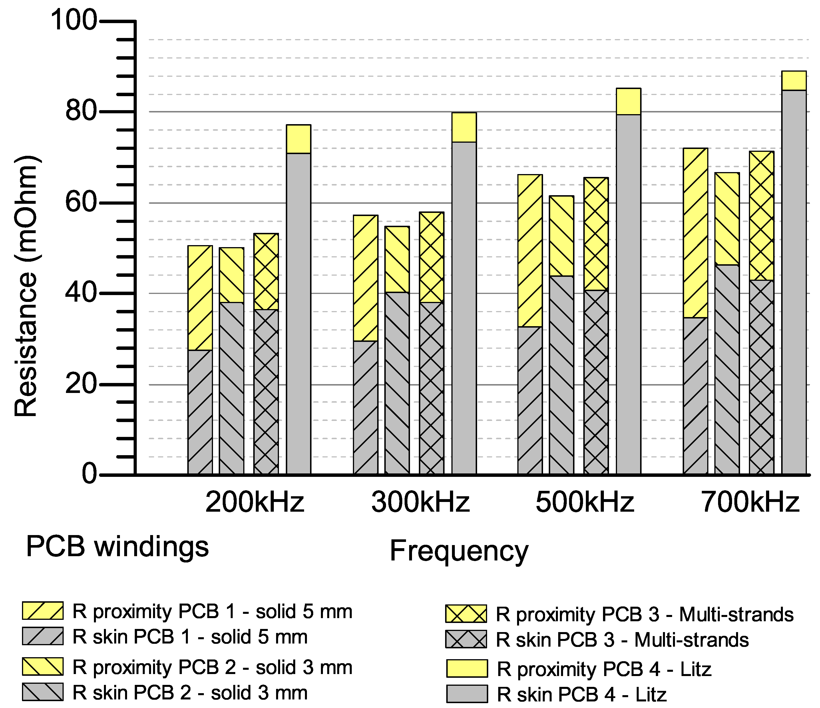
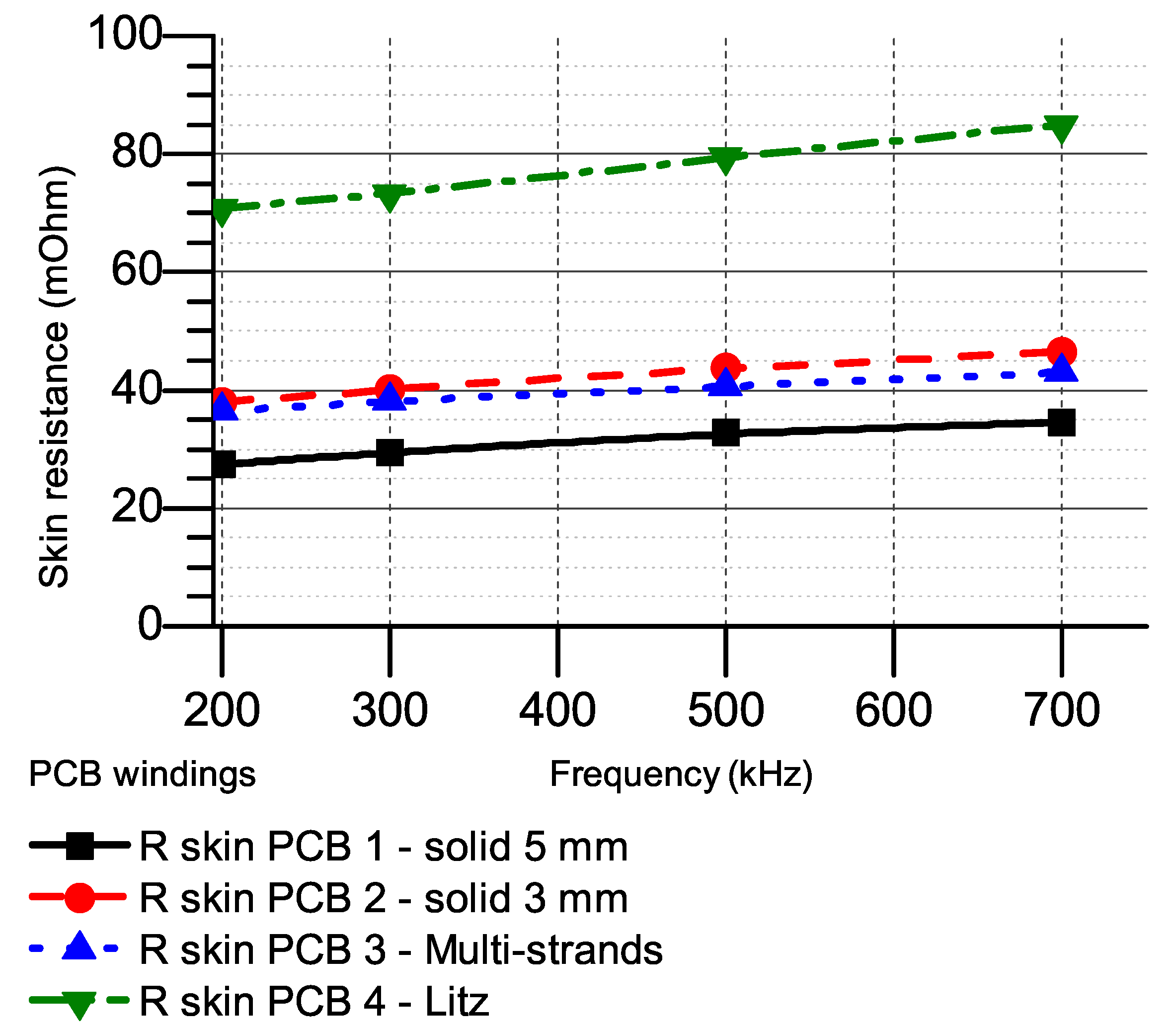
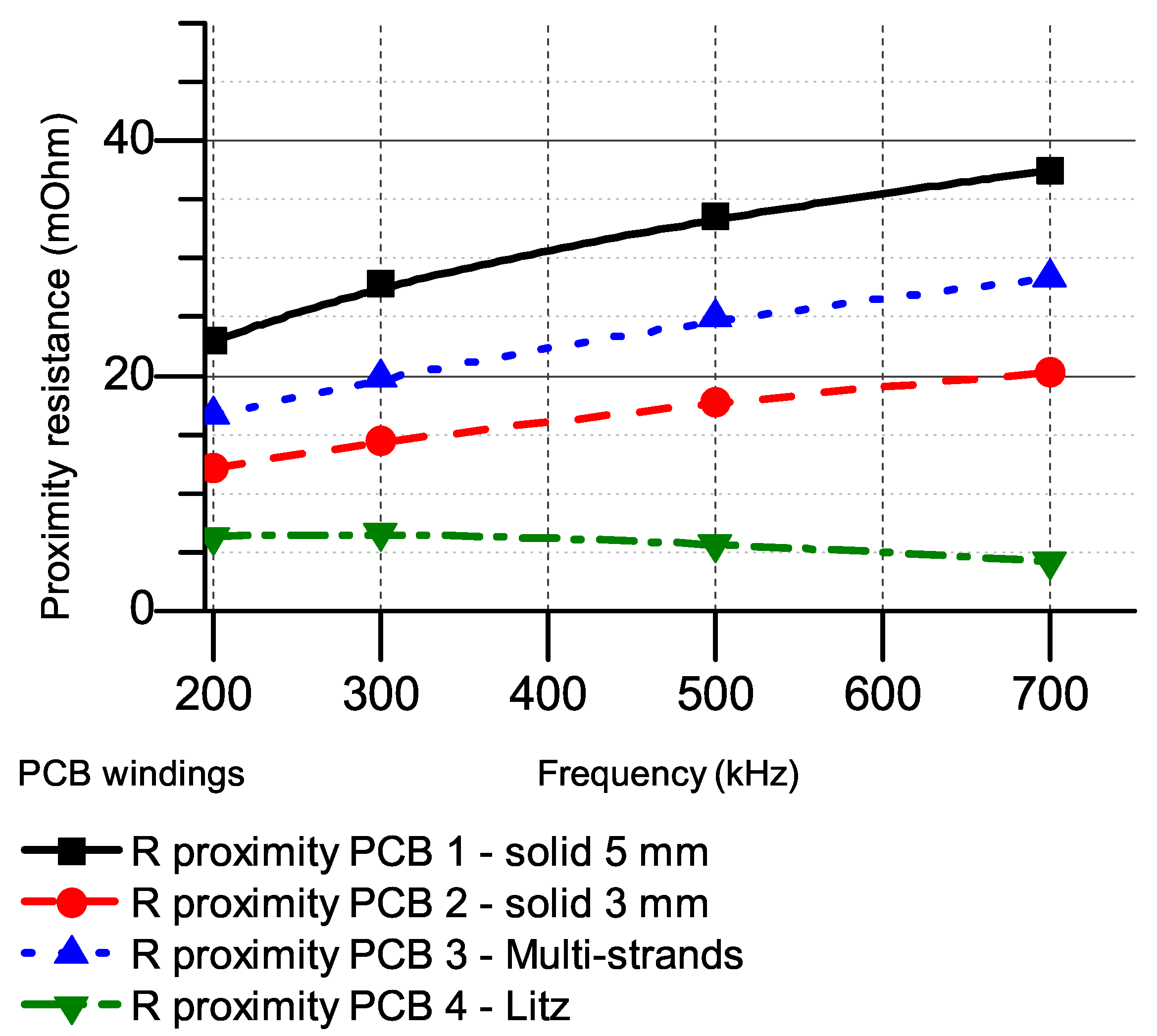
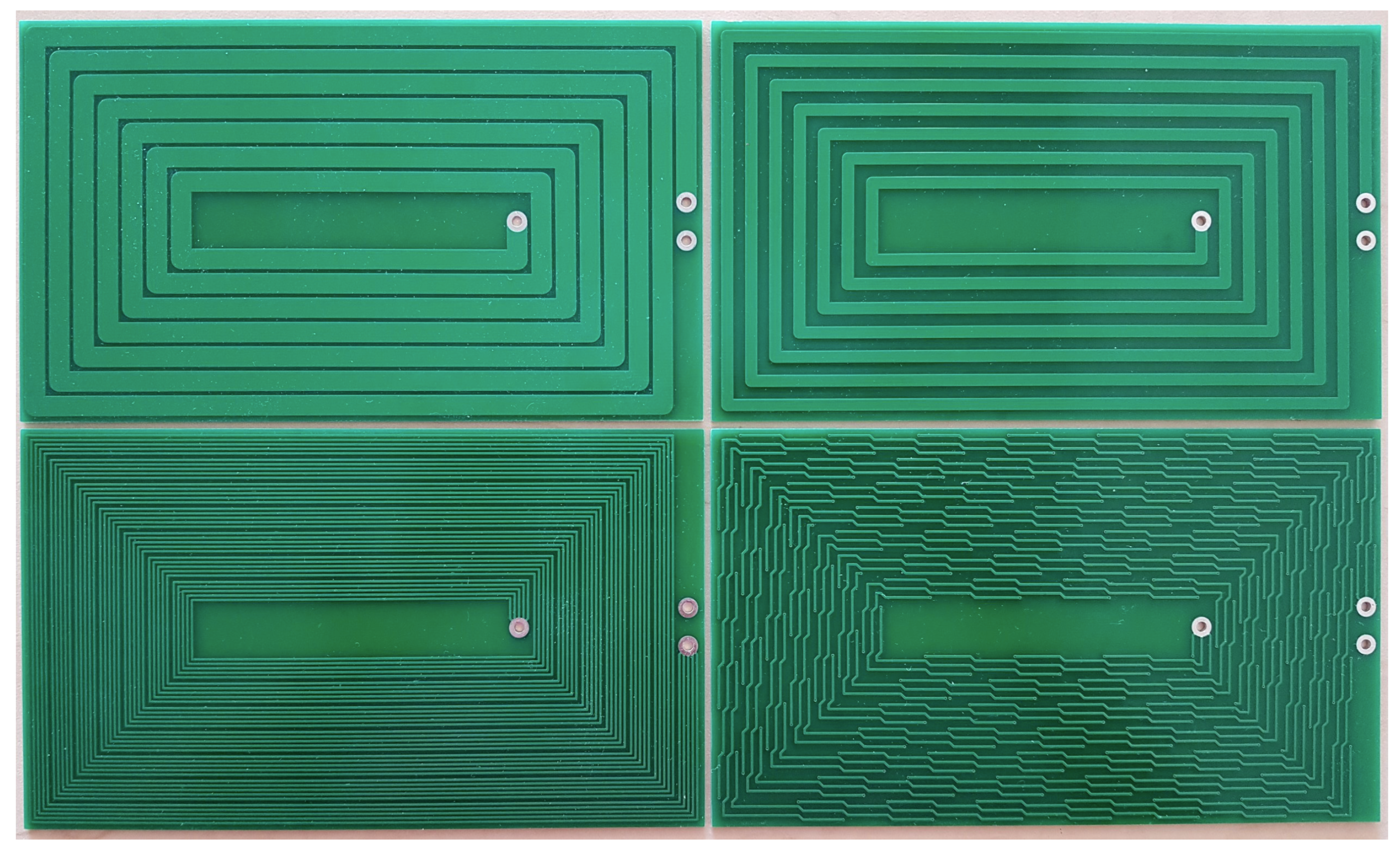
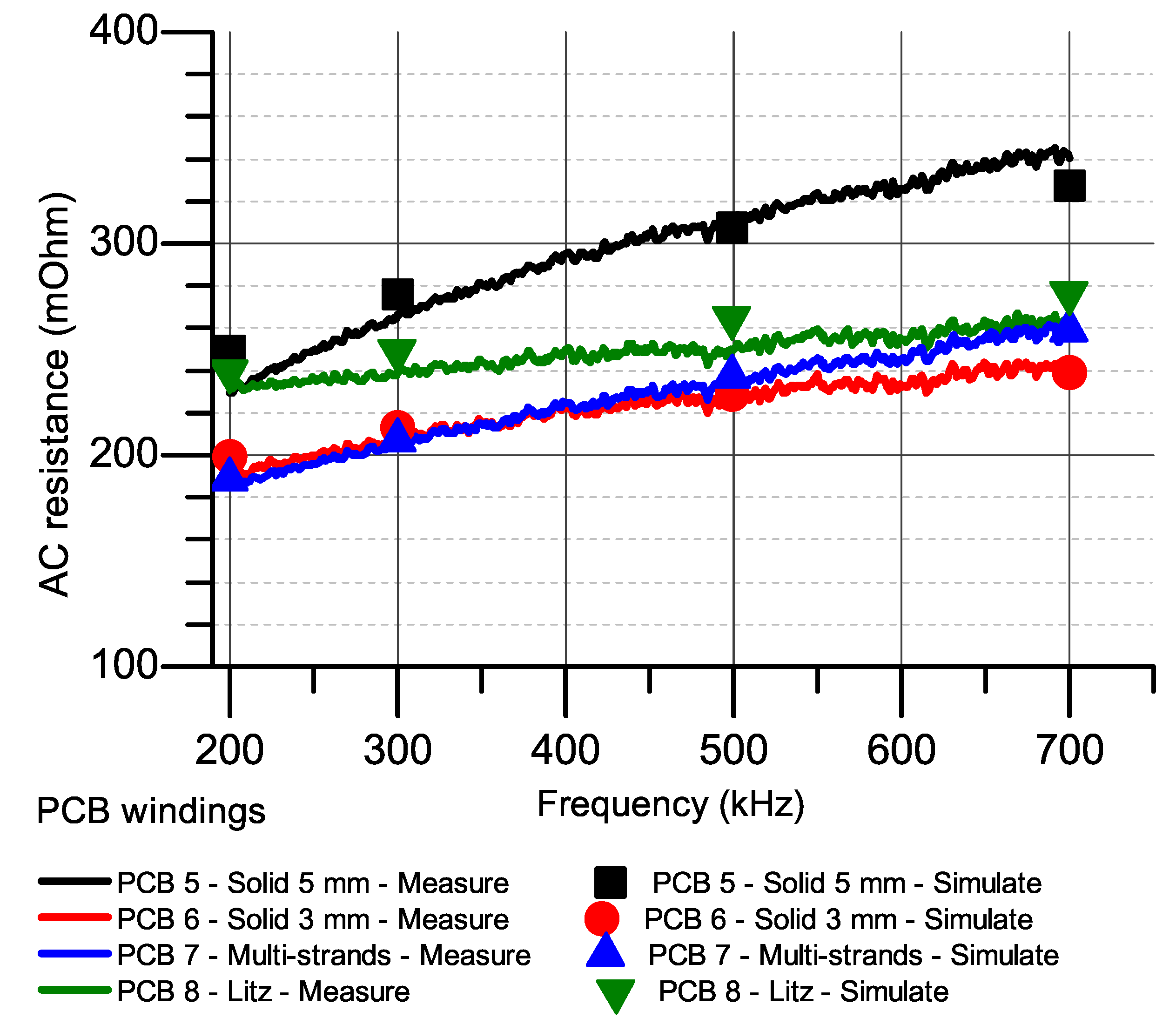
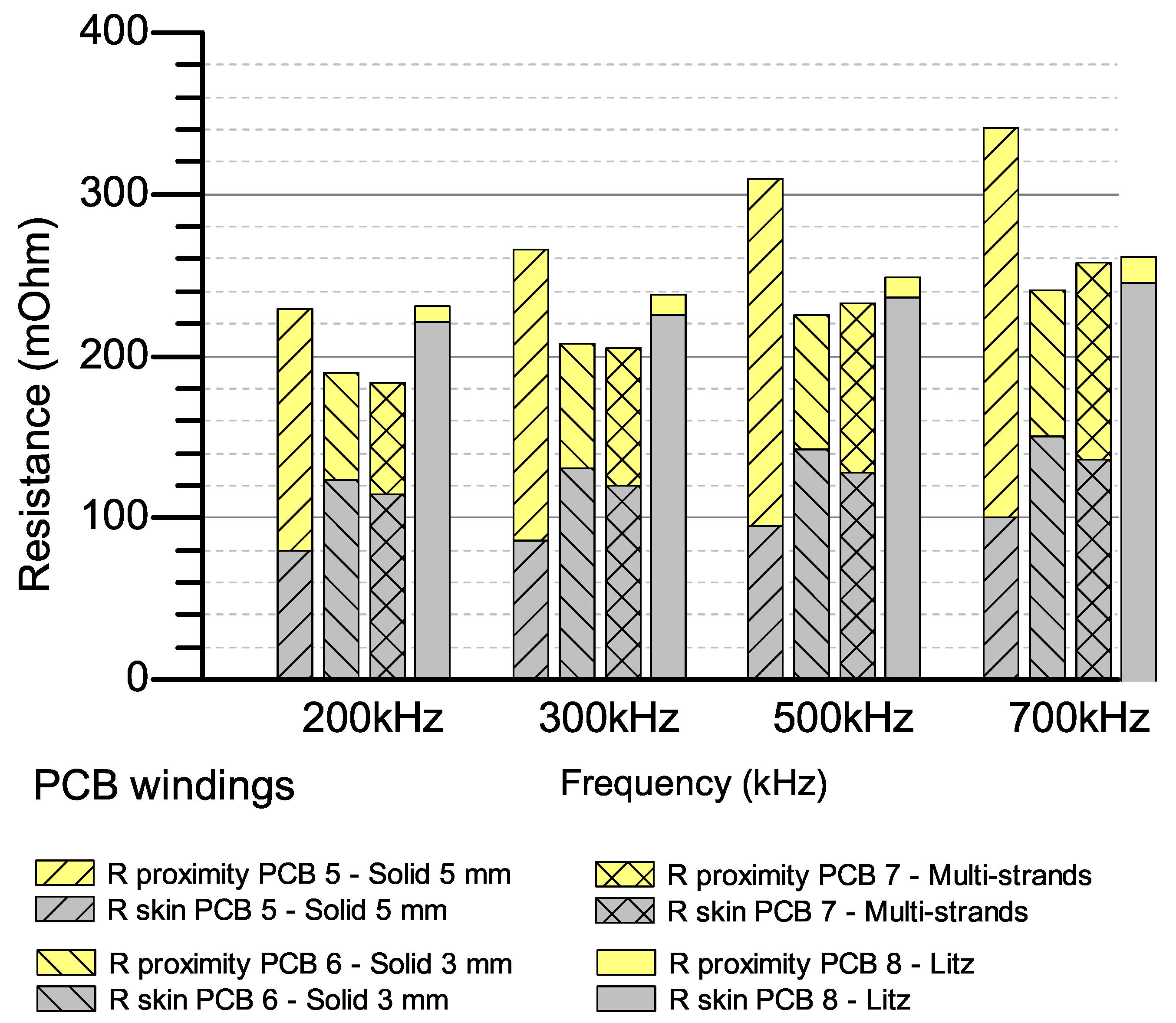
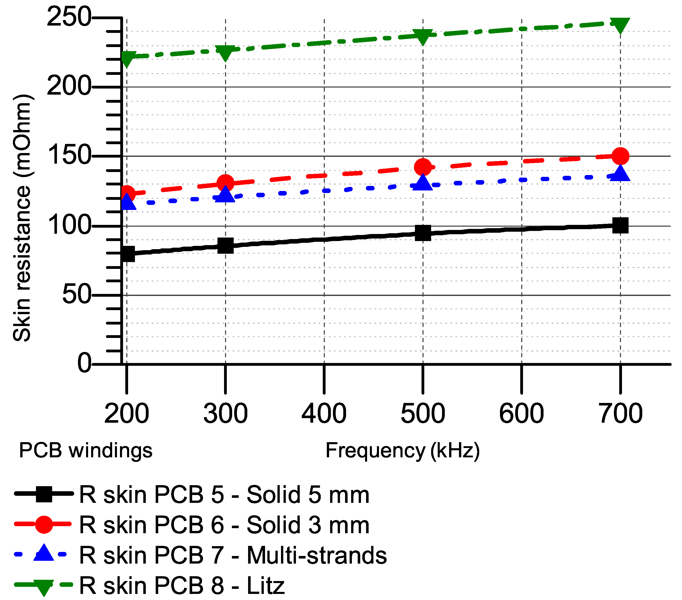
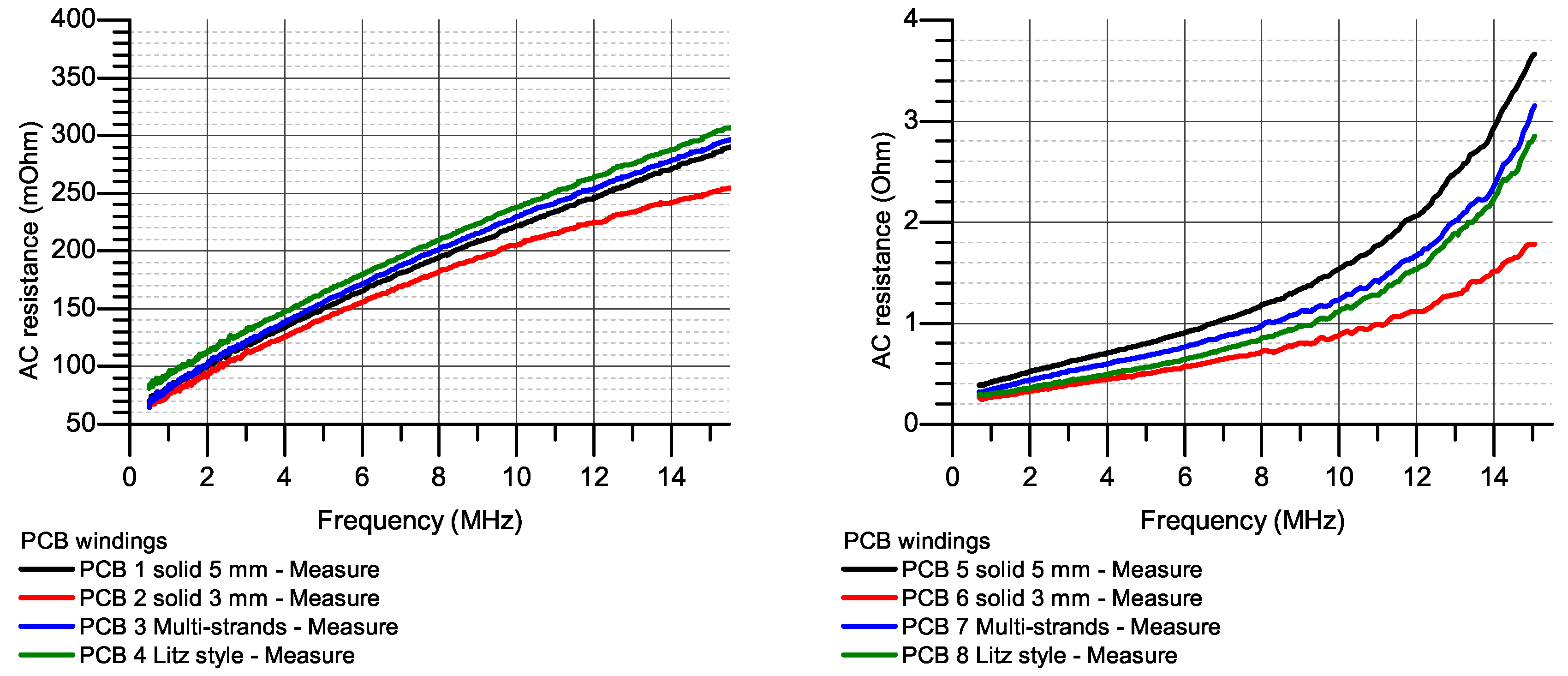
3.3. Case Study 3: 7-Turn 2-Layer PCB Windings
4. Discussion
4.1. AC Resistances at Higher Frequency
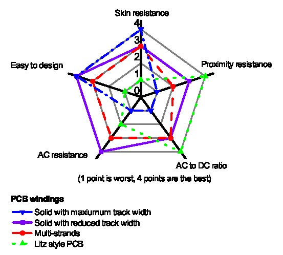
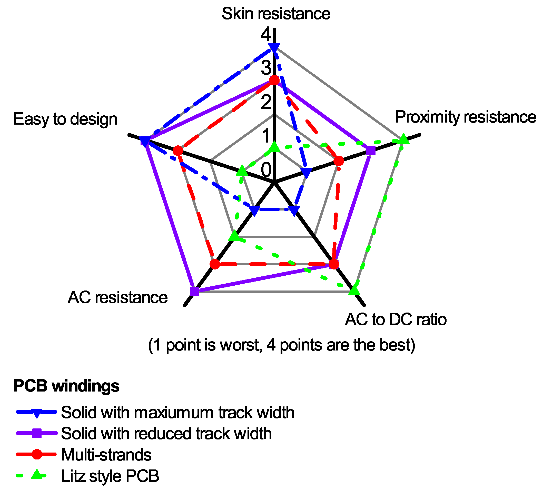
4.2. Pros and Cons of Each Winding Style
5. Conclusions
Author Contributions
Funding
Conflicts of Interest
Abbreviations
| Copper conductivity | |
| Copper skin depth | |
| Angular frequency | |
| Average external magnetic field parallel to X Axis | |
| Average external magnetic field parallel to Z Axis | |
| d | Strand width |
| FEM | Finite element simulation |
| Ratio of AC resistance causes by skin effect to DC resistance | |
| Ratio of AC resistance causes by proximity effect to DC resistance | |
| Ratio of total AC resistance to DC resistance | |
| h | Track thickness |
| I | Excitation current or main current |
| Outer length of a winding | |
| MMF | Magnetomotive Force |
| N | Number of strands of one layer of multi-strand winding or Number of strands of Litz style winding |
| Total number of strands of a winding | |
| P | Track pitch |
| Total AC resistance causes by skin and proximity effects | |
| DC resistance | |
| AC resistance causes by skin effect | |
| AC resistance causes by proximity effect | |
| S | Track distance |
| t | PCB thickness or layer distance |
| VNA | Vector Network Analyzer |
| W | Track width |
| Outer width of a winding |
References
- Li, B.; Li, Q.; Lee, F.C. High-Frequency PCB Winding Transformer With Integrated Inductors for a Bi-Directional Resonant Converter. IEEE Trans. Ind. Electron. 2019, 34, 6123–6135. [Google Scholar] [CrossRef]
- Ouyang, Z.; Thomsen, O.C.; Andersen, M.A.E. Optimal Design and Tradeoff Analysis of Planar Transformer in High-Power DC–DC Converters. IEEE Trans. Ind. Electron. 2012, 59, 2800–2810. [Google Scholar] [CrossRef]
- Marian, K. Kazimierczuk, Proximity Effect. In High Frequency Magnetic Components, 2nd ed.; Wiley: Coshocton, OH, USA, 2014; p. 226. [Google Scholar]
- Barrios, E.L.; Urtasun, A.; Ursúa, A.; Marroyo, L.; Sanchis, P. High-Frequency Power Transformers with Foil Windings: Maximum Interleaving and Optimal Design. IEEE Trans. Ind. Electron. 2015, 30, 5712–5723. [Google Scholar] [CrossRef]
- Zhao, B.; Ouyang, Z.; Anderson, M.A.E.; Duffy, M.; Hurley, W.G. An improved partially interleaved transformer structure for high-voltage high-frequency multiple-output applications. In Proceedings of the IECON 2017-43rd Annual Conference of the IEEE Industrial Electronics Society, Beijing, China, 29 October–1 November 2017; pp. 798–804. [Google Scholar]
- Youssouf, K.; Kahlouche, F.; Soultan, M.; Youssouf, M.; Bechir, M.H.; Capraro, S.; Chatelon, J.P.; Siblini, A.; Siblini, J.J. Design and Study of Interleaved and Face to Face Magnetic Microtransformers. IEEE Trans. Electron. Devices 2014, 61, 2873–2878. [Google Scholar] [CrossRef]
- Thummala, P.; Schneider, H.; Zhang, Z.; Andersen, M.A.E. Investigation of Transformer Winding Architectures for High-Voltage (2.5 kV) Capacitor Charging and Discharging Applications. IEEE Trans. Ind. Electron. 2016, 31, 5786–5796. [Google Scholar] [CrossRef]
- Lee, C.K.; Su, Y.P.; Hui, S.Y.R. Printed Spiral Winding Inductor With Wide Frequency Bandwidth. IEEE Trans. Ind. Electron. 2011, 26, 2936–2945. [Google Scholar] [CrossRef] [Green Version]
- Saket, M.A.; Shafiei, N.; Ordonez, M. Planar transformer winding technique for reduced capacitance in LLC power converters. In Proceedings of the 2016 IEEE Energy Conversion Congress and Exposition (ECCE), Milwaukee, WI, USA, 18–22 September 2016; pp. 1–6. [Google Scholar] [CrossRef]
- Stadler, A.; Albach, M.; Macary, F. The minimization of copper losses in core-less inductors: Application to foil- and PCB-based planar windings. In Proceedings of the 2005 European Conference on Power Electronics and Applications, Dresden, Germany, 11–14 September 2005. [Google Scholar] [CrossRef]
- Marian, K. Kazimierczuk, Winding resistance at high frequencies. In High Frequency Magnetic Components, 2nd ed.; Wiley: Coshocton, OH, USA, 2014; p. 303. [Google Scholar]
- Su, Y.; Liu, X.; Lee, C.K.; Hui, S.Y. On the relationship of quality factor and hollow winding structure of coreless printed spiral winding (CPSW) inductor. IEEE Trans. Ind. Electron. 2012, 27, 3050–3056. [Google Scholar]
- Kim, D.-H.; Park, Y.-J. Calculation of the inductance and AC resistance of planar rectangular coils. Electron. Lett. 2016, 52, 1321–1323. [Google Scholar] [CrossRef]
- Nguyen, M.H.; Fortin Blanchette, H. Optimizing AC Resistance of Solid PCB Winding. Electronics 2020, 9, 875. [Google Scholar] [CrossRef]
- Varghese, B.J.; Smith, T.; Azad, A.; Pantic, Z. Design and optimization of decoupled concentric and coplanar coils for WPT systems. In Proceedings of the 2017 IEEE Wireless Power Transfer Conference (WPTC), Taipei, Taiwan, 10–12 May 2017; pp. 1–4. [Google Scholar]
- Lope, I.; Carretero, C.; Acero, J.; Burdío, J.M.; Alonso, R. PCB multi-track coils for domestic induction heating applications. In Proceedings of the IECON 2012-38th Annual Conference on IEEE Industrial Electronics Society, Montreal, QC, Canada, 25–28 October 2012; pp. 3287–3292. [Google Scholar]
- Serrano, J.; Lope, I.; Acero, J.; Carretero, C.; Burdío, J.M. Mathematical description of PCB-adapted litz wire geometry for automated layout generation of WPT coils. In Proceedings of the IECON 2017-43rd Annual Conference of the IEEE Industrial Electronics Society, Beijing, China, 29 October–1 November 2017; pp. 6955–6960. [Google Scholar]
- Lope, I.; Carretero, C.; Acero, J.; Alonso, R.; Burdío, J.M. AC Power Losses Model for Planar Windings with Rectangular Cross-Sectional Conductors. IEEE Trans. Ind. Electron. 2014, 29, 23–28. [Google Scholar] [CrossRef]
- Wang, S.; de Rooij, M.A.; Odendaal, W.G.; van Wyk, J.D.; Boroyevich, D. Reduction of high-frequency conduction losses using a planar litz structure. IEEE Trans. Ind. Electron. 2005, 20, 261–267. [Google Scholar] [CrossRef]
- Lope, I.; Acero, J.; Serrano, J.; Carretero, C.; Alonso, R.; Burdio, J.M. Minimization of vias in PCB implementations of planar coils with litz-wire structure. In Proceedings of the 2015 IEEE Applied Power Electronics Conference and Exposition (APEC), Charlotte, NC, USA, 15–19 March 2015; pp. 2512–2517. [Google Scholar]
- Rehlaender, P.; Grote, T.; Tikhonov, S.; Niejende, H.; Schafmeister, F.; Bocker, J.; Thiemann, P. A PCB Integrated Winding Using a Litz Structure for a Wireless Charging Coil. In Proceedings of the 2019 21st European Conference on Power Electronics and Applications (EPE’19 ECCE Europe), Genova, Italy, 2–5 September 2019; pp. pp. P.1–P.9.
- Kuhn, W.B.; Ibrahim, N.M. Analysis of current crowding effects in multiturn spiral inductors. IEEE Trans. Microw. Theory Tech. 2001, 49, 31–38. [Google Scholar] [CrossRef] [Green Version]
- Hurley, W.G.; Gath, E.; Breslin, J.G. Optimizing the AC resistance of multilayer transformer windings with arbitrary current waveforms. IEEE Trans. Ind. Electron. 2000, 15, 369–376. [Google Scholar] [CrossRef] [Green Version]
- Lope, I.; Carretero, C.; Acero, J.; Alonso, R.; Burdio, J.M. Frequency-Dependent Resistance of Planar Coils in Printed Circuit Board With Litz Structure. IEEE Trans. Magn. 2014, 50, 8402409. [Google Scholar] [CrossRef]


| No | Profile Names | Track Width | Track Pitch | Strand Width | Total Number of Strands |
|---|---|---|---|---|---|
| PCB1 | Solid with maximum track width | P | - | - | |
| PCB2 | Solid with reduced track width | P | - | - | |
| PCB3 | Multi-strands | P | d | 2N | |
| PCB4 | Litz style PCB | P | d | N |
| No | Profile Names | DC Resistance | Skin Resistance | Proximity Resistance |
|---|---|---|---|---|
| PCB1 | Solid with maximum track width | |||
| PCB2 | Solid with reduced track width | |||
| PCB3 | Multi-strands | |||
| PCB4 | Litz style PCB |
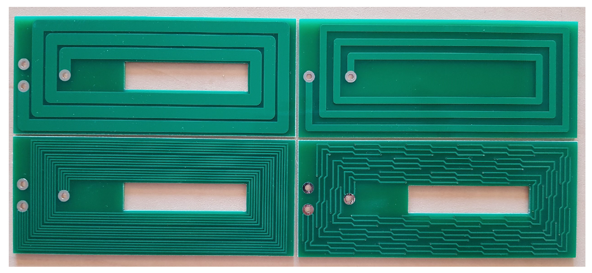
| Group | No | Descriptions | Number of Turns | Outer Length | Outer Width | Track Width | Strand Width | Total Number of Strands |
|---|---|---|---|---|---|---|---|---|
| Group 1 | PCB 1 | Solid winding 2 layers | 3 | 112 | 43 | 5 | - | - |
| PCB 2 | Solid winding 2 layers | 3 | 112 | 43 | 3 | - | - | |
| PCB 3 | Multi-strands winding 2 layers | 3 | 112 | 43 | 5 | 0.6 | 10 | |
| PCB 4 | Litz winding 2 layers | 3 | 112 | 43 | 5 | 0.6 | 5 | |
| Group 2 | PCB 5 | Solid winding 2 layers | 7 | 160 | 91 | 5 | - | - |
| PCB 6 | Solid winding 2 layers | 7 | 160 | 91 | 3 | - | - | |
| PCB 7 | Multi-strands winding 2 layers | 7 | 160 | 91 | 5 | 0.6 | 10 | |
| PCB 8 | Litz winding 2 layers | 7 | 160 | 91 | 5 | 0.6 | 5 | |
| Group 3 | PCB 9 | Solid winding 1 layer | 1 | 160 | 91 | 5 | - | - |
| PCB 10 | Solid winding 1 layer | 1 | 160 | 91 | 3 | - | - | |
| PCB 11 | Multi-strands winding 1 layer | 1 | 160 | 91 | 5 | 0.6 | 5 | |
| PCB 12 | Litz winding 2 layers | 1 | 160 | 91 | 5 | 0.6 | 5 |
| Group | PCBs | Descriptions | m | m | m |
|---|---|---|---|---|---|
| Group 1 (Three-Turn PCBs) | PCB 1 | solid 5 mm | 22.5 | 21.28 | 0.7 |
| PCB 2 | solid 3 mm | 33.1 | 34.78 | 1.68 | |
| PCB 3 | multi-strands | 38.2 | 35.27 | 2.93 | |
| PCB 4 | Litz PCB | 74 | 70.57 | 3.43 | |
| Group 2 (Seven-Turn PCBs) | PCB 5 | solid 5 mm | 65.3 | 69.83 | 4.53 |
| PCB 6 | solid 3 mm | 107.1 | 114 | 6.9 | |
| PCB 7 | multi-strands | 107.96 | 114.5 | 6.54 | |
| PCB 8 | Litz PCB | 222 | 226.64 | 4.64 | |
| Group 3 (One-Turn PCBs) | PCB 9 | solid 5 mm | 24.57 | 26.5 | 1.93 |
| PCB 10 | solid 3 mm | 43.2 | 44.1 | 0.9 | |
| PCB 11 | multi-strands | 39.76 | 43.54 | 3.78 | |
| PCB 12 | Litz PCB | 38.61 | 44.89 | 6.28 |
© 2020 by the authors. Licensee MDPI, Basel, Switzerland. This article is an open access article distributed under the terms and conditions of the Creative Commons Attribution (CC BY) license (http://creativecommons.org/licenses/by/4.0/).
Share and Cite
Nguyen, M.H.; Fortin Blanchette, H. A Review and Comparison of Solid, Multi-Strands and Litz Style PCB Winding. Electronics 2020, 9, 1324. https://doi.org/10.3390/electronics9081324
Nguyen MH, Fortin Blanchette H. A Review and Comparison of Solid, Multi-Strands and Litz Style PCB Winding. Electronics. 2020; 9(8):1324. https://doi.org/10.3390/electronics9081324
Chicago/Turabian StyleNguyen, Minh Huy, and Handy Fortin Blanchette. 2020. "A Review and Comparison of Solid, Multi-Strands and Litz Style PCB Winding" Electronics 9, no. 8: 1324. https://doi.org/10.3390/electronics9081324