An Energy-Efficient Integration of a Digital Modulator and a Class-D Amplifier


Abstract
:1. Introduction
2. State-of-the-Art
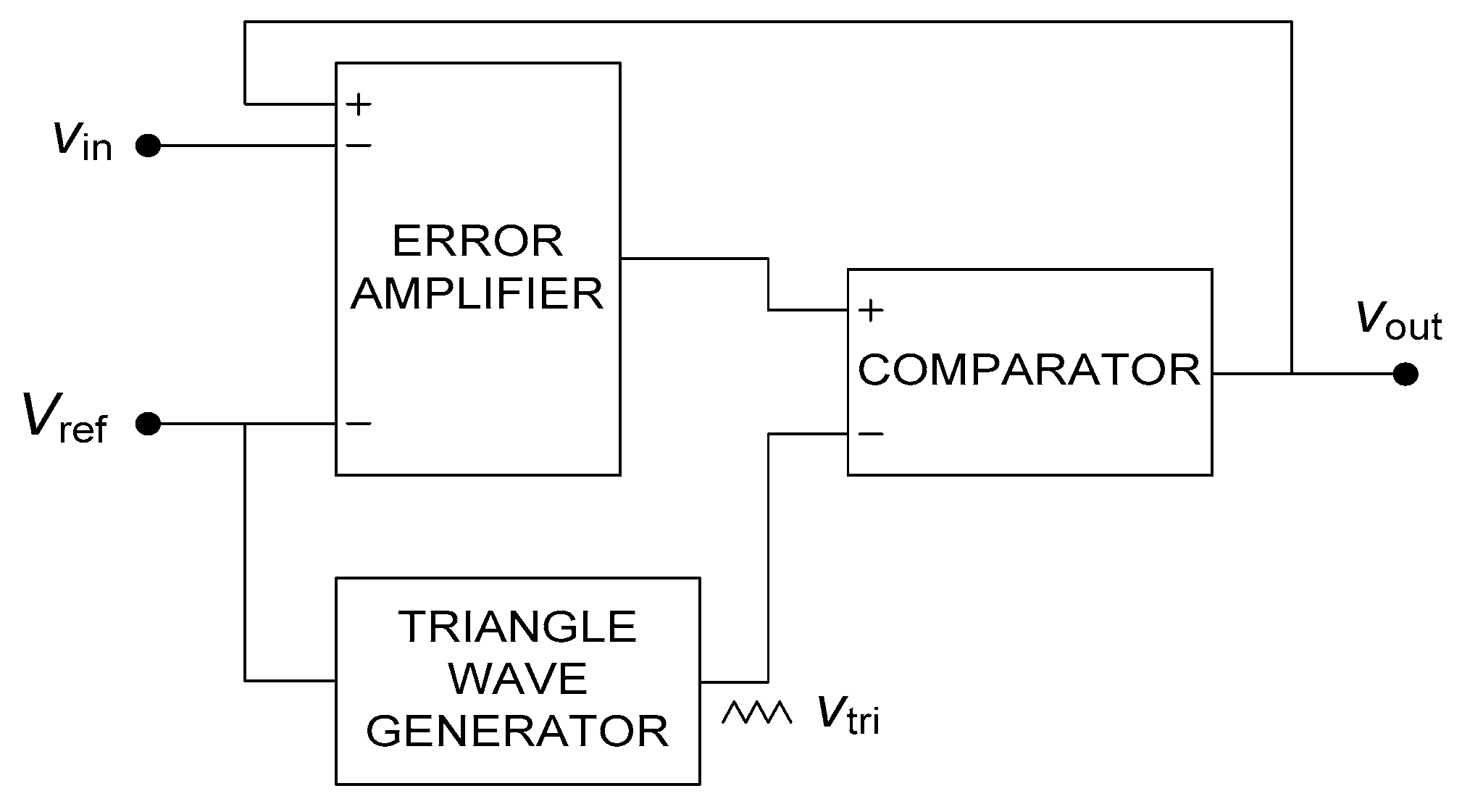
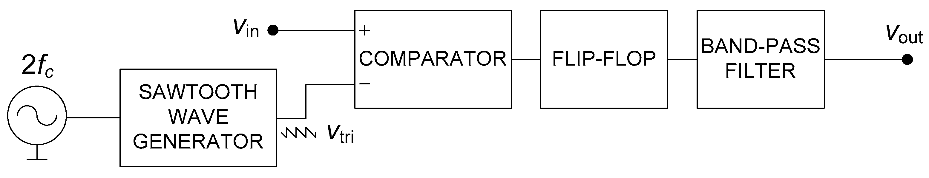
3. Theoretical Background
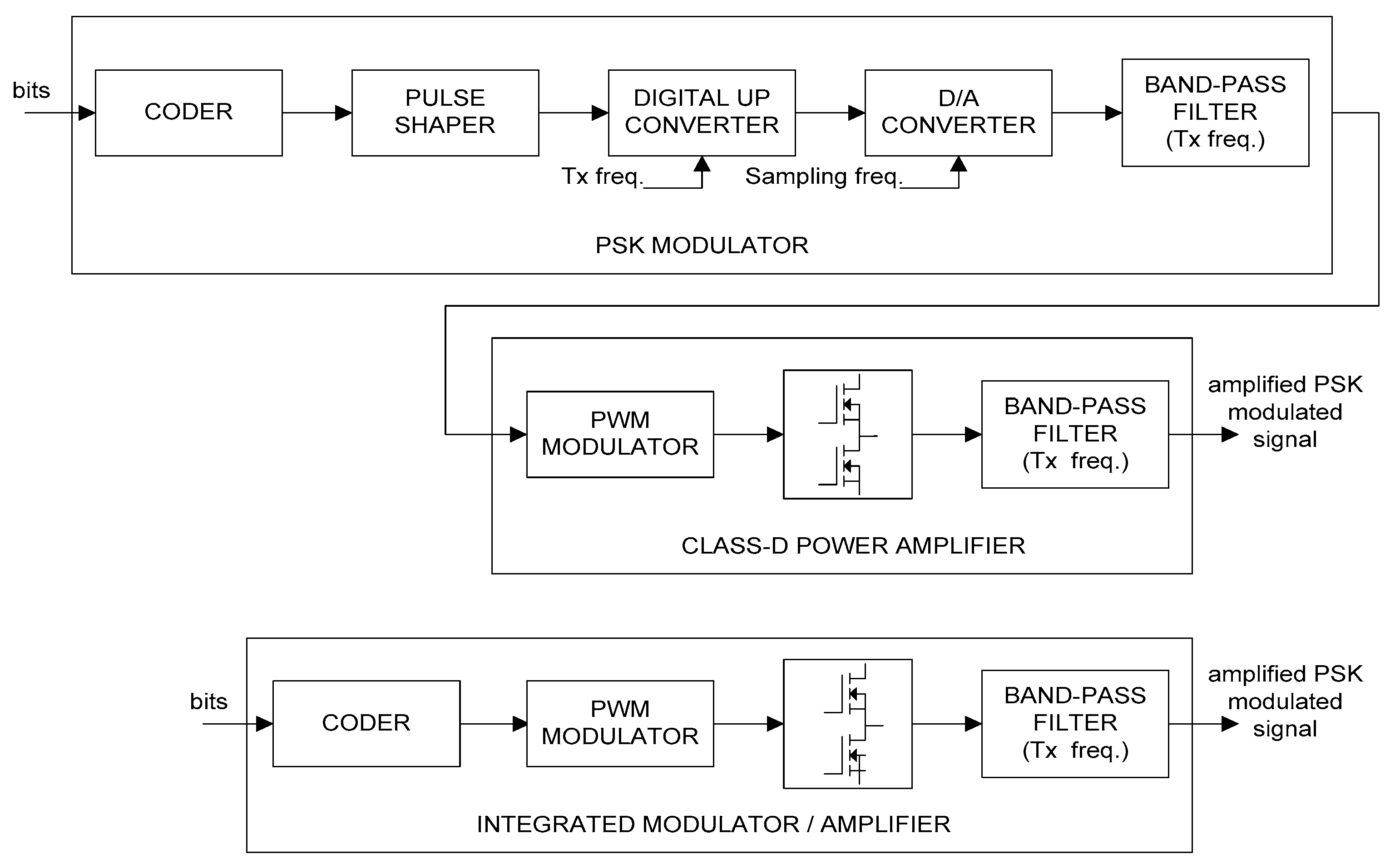
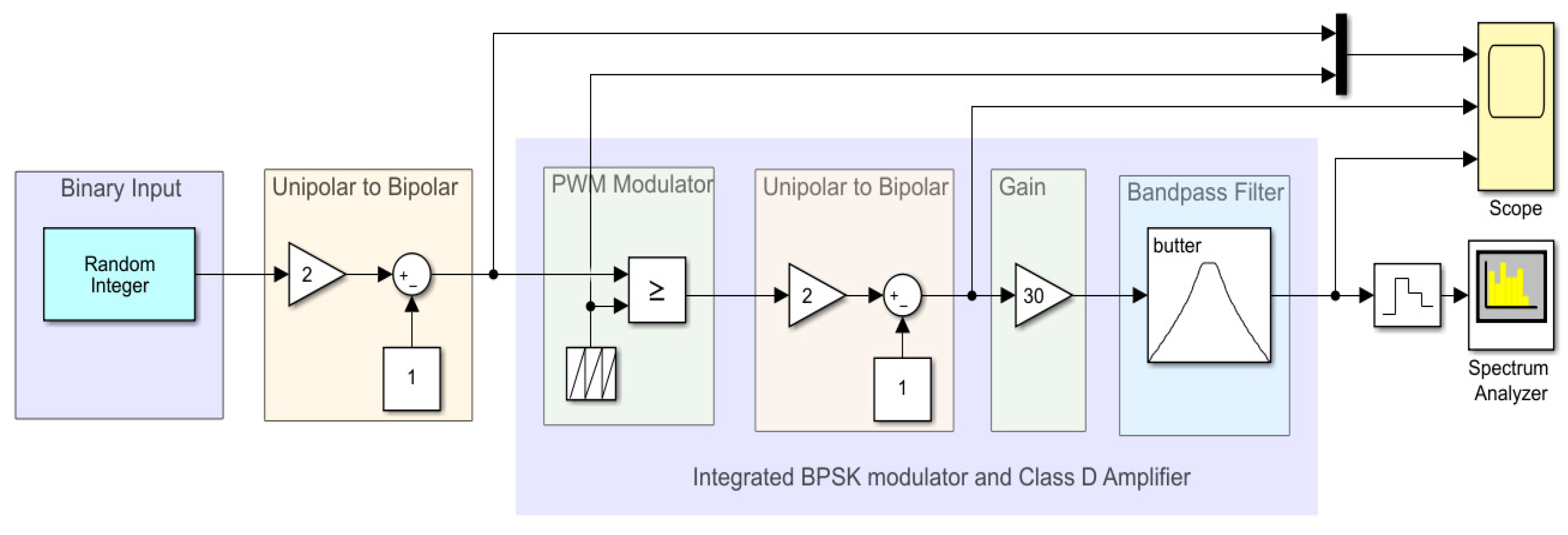
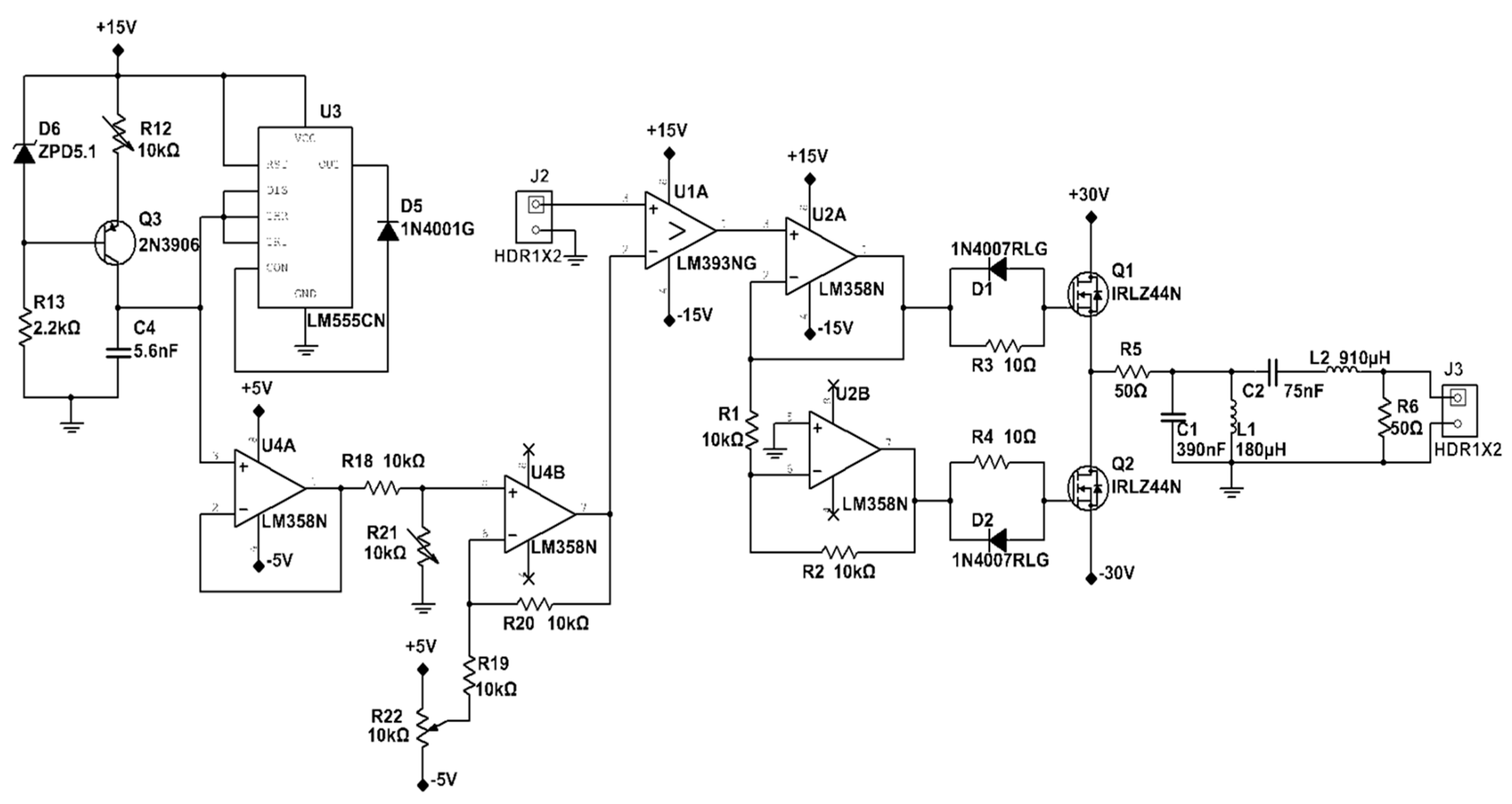
4. Block Diagram of the Integrated System
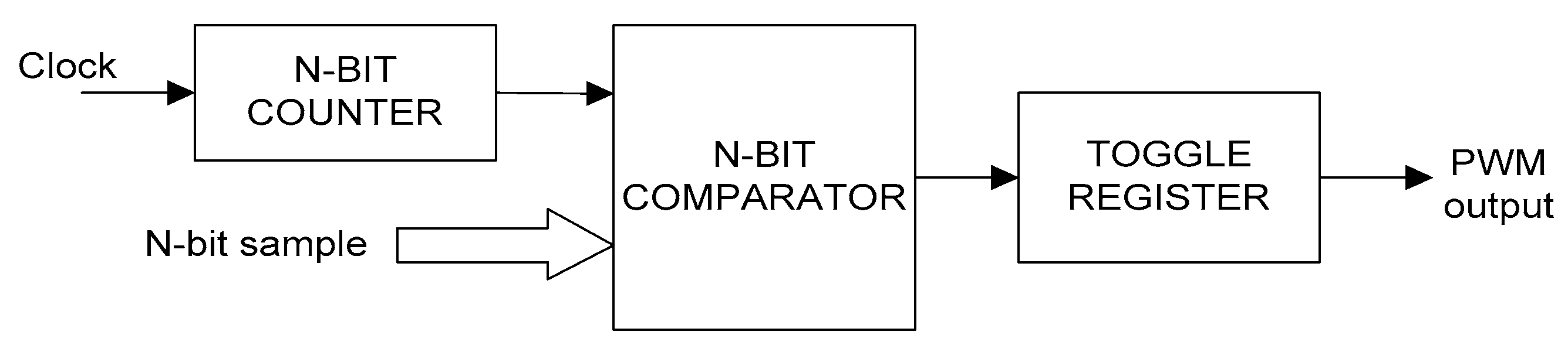
4.1. Preferred Modulation
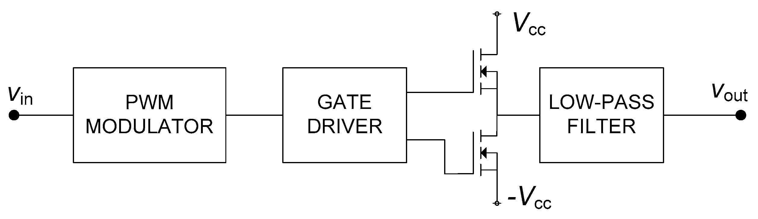
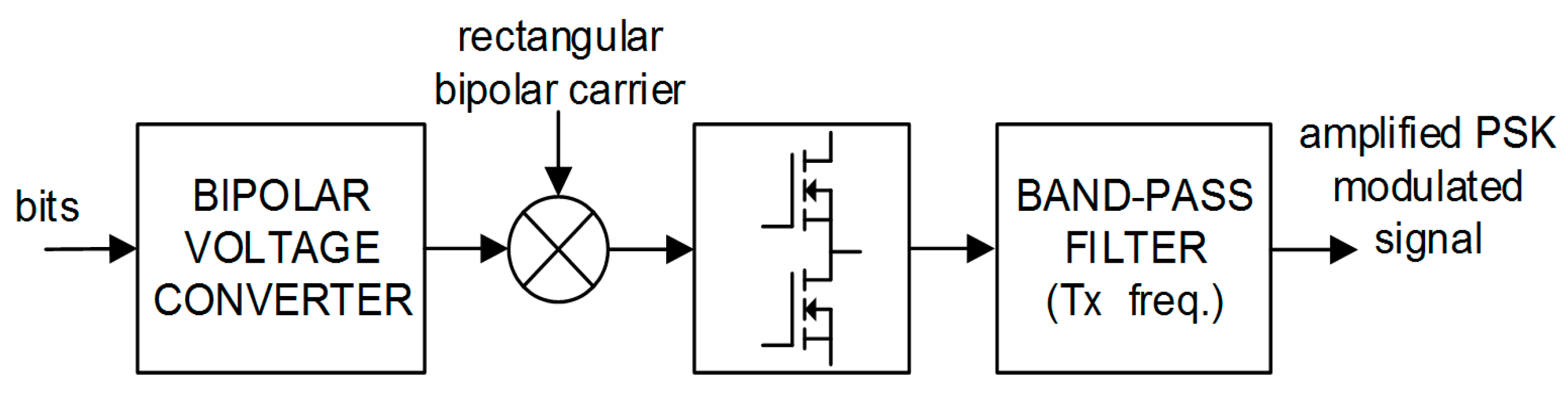
4.2. Integrated System
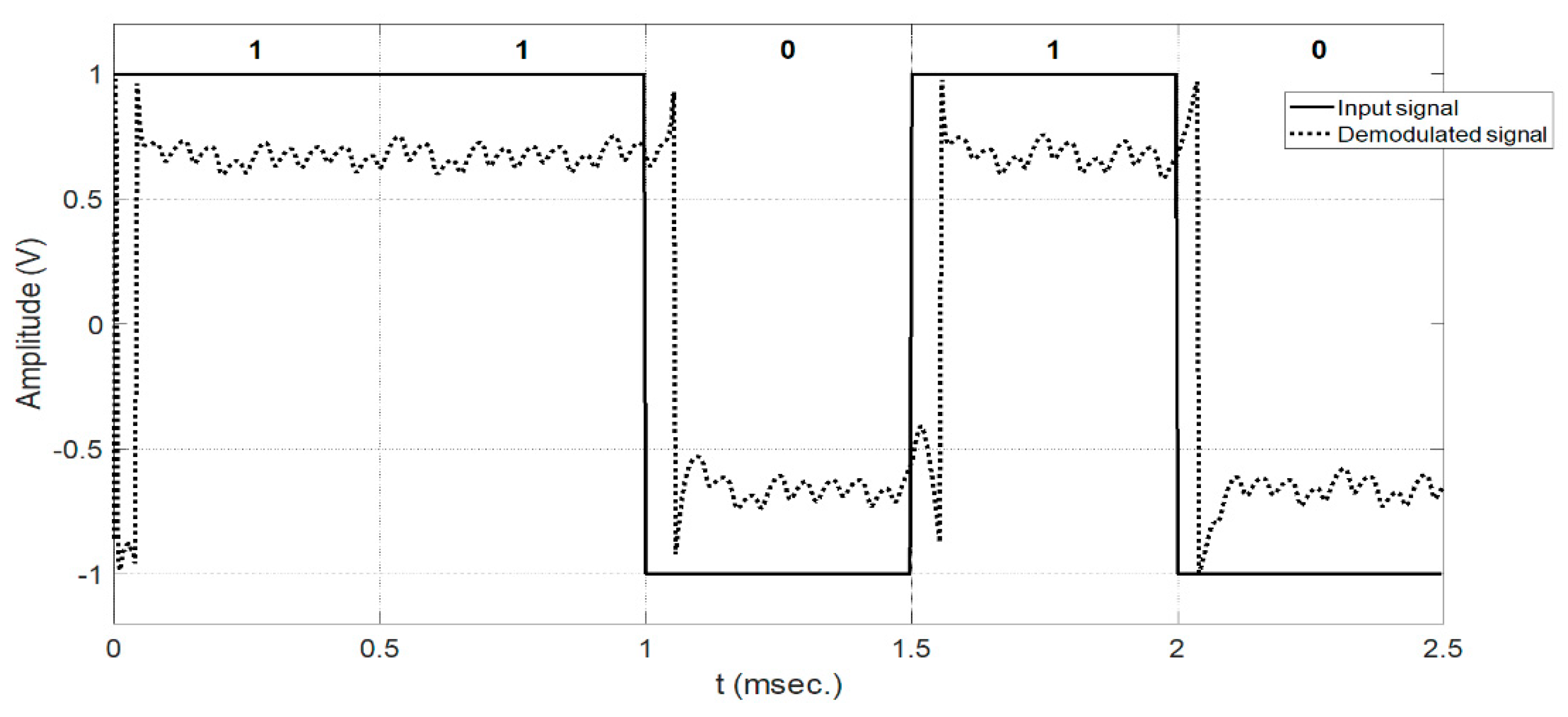
5. Experimental Setup and Results
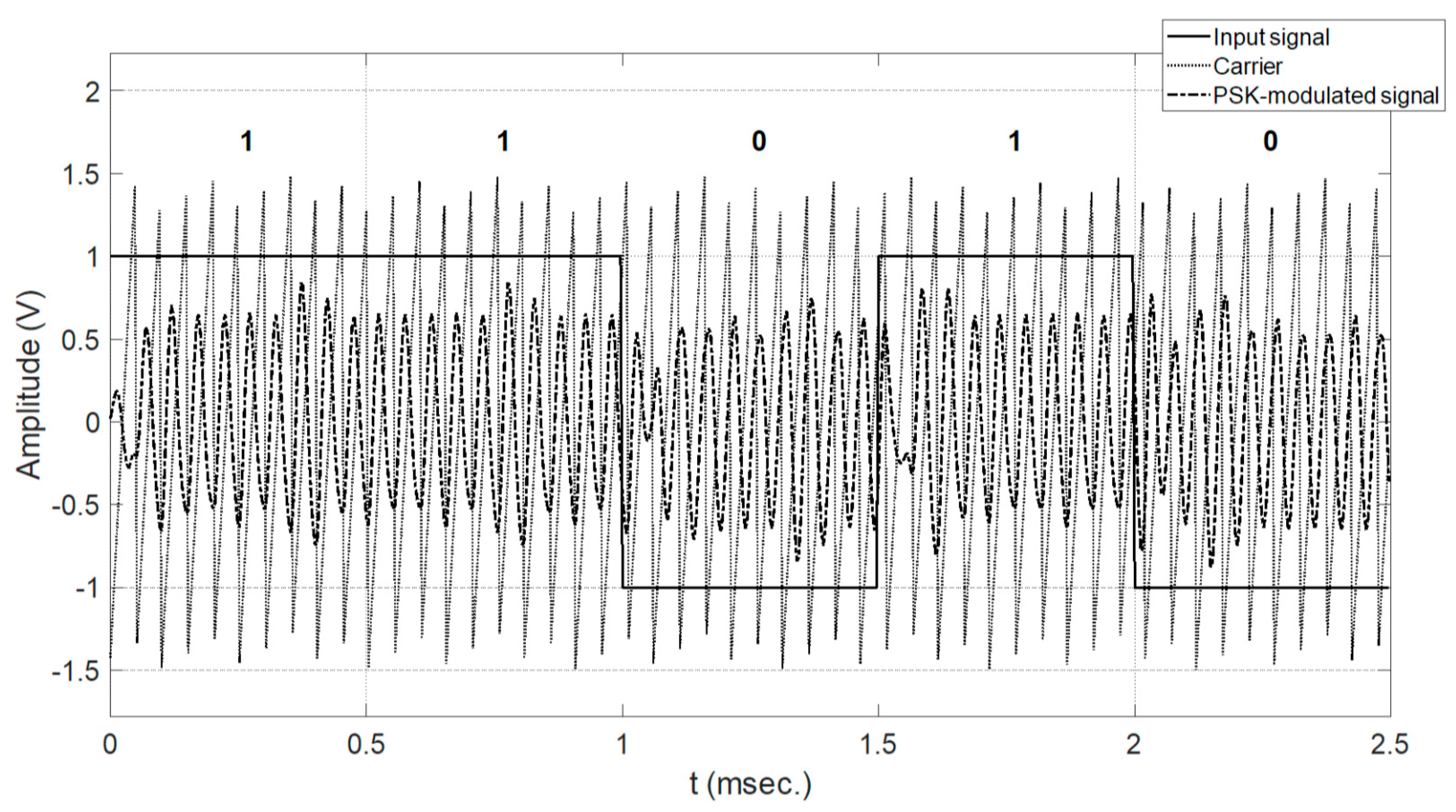
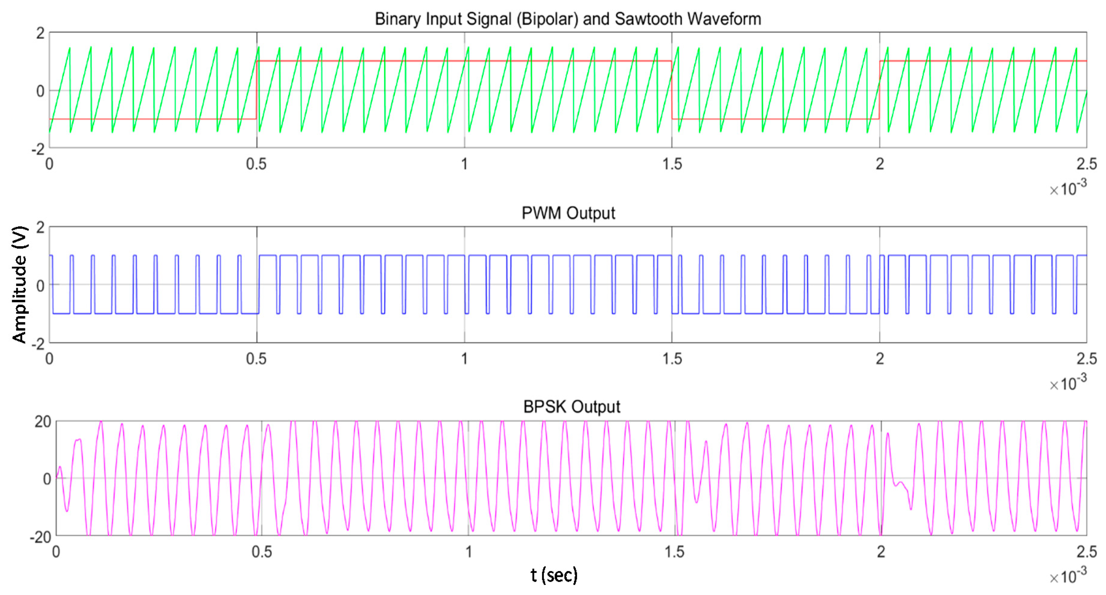
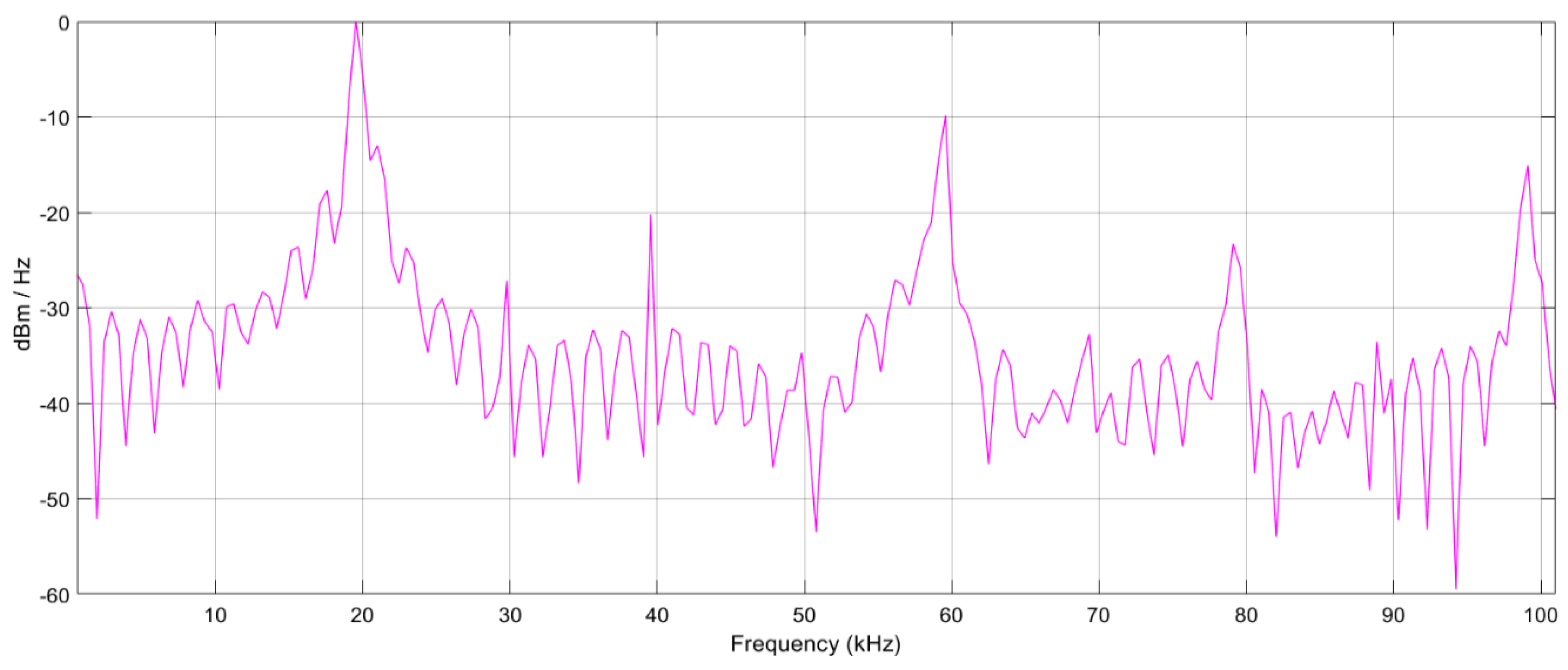
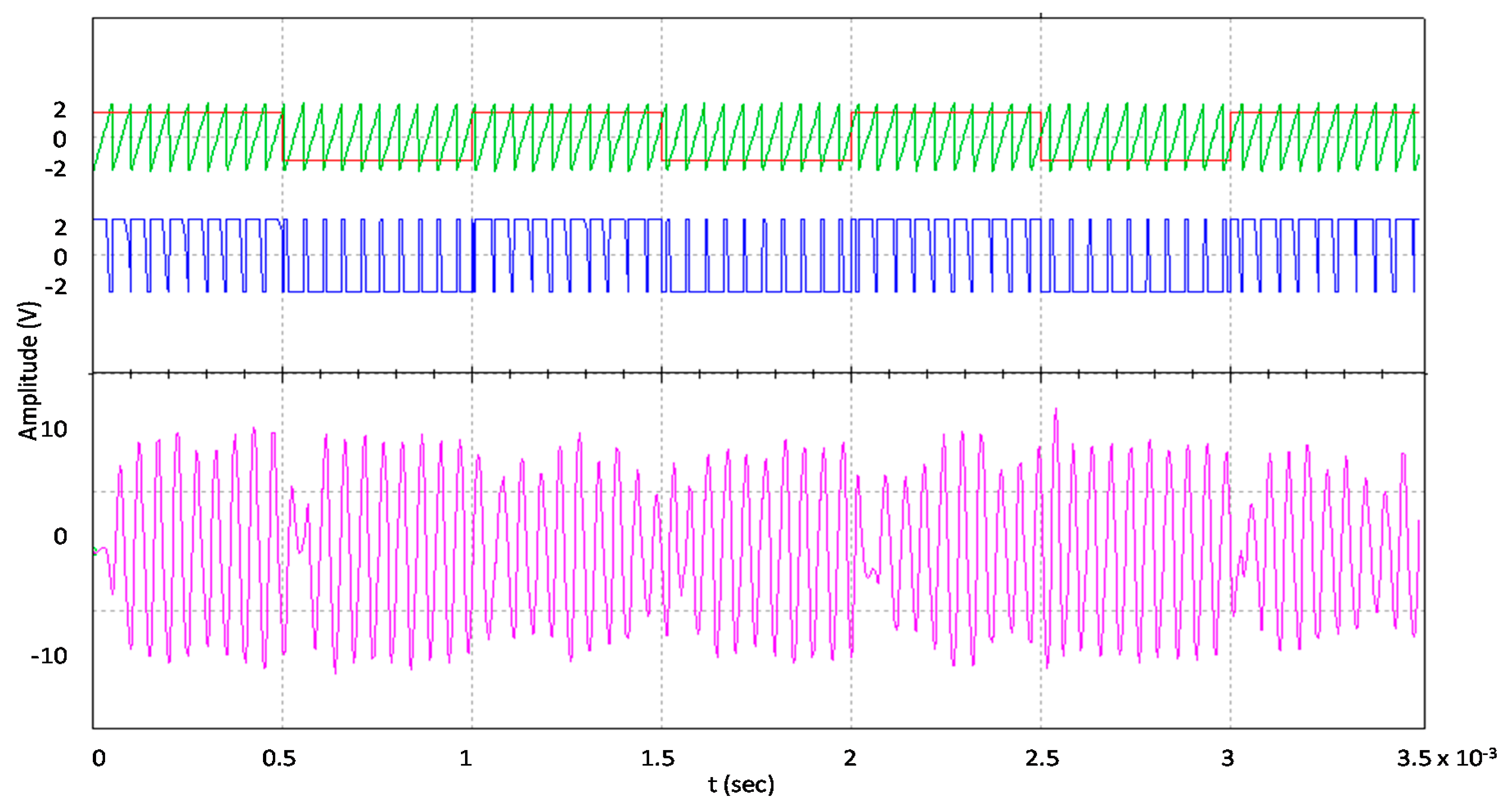
5.1. Simulation
5.2. Prototype
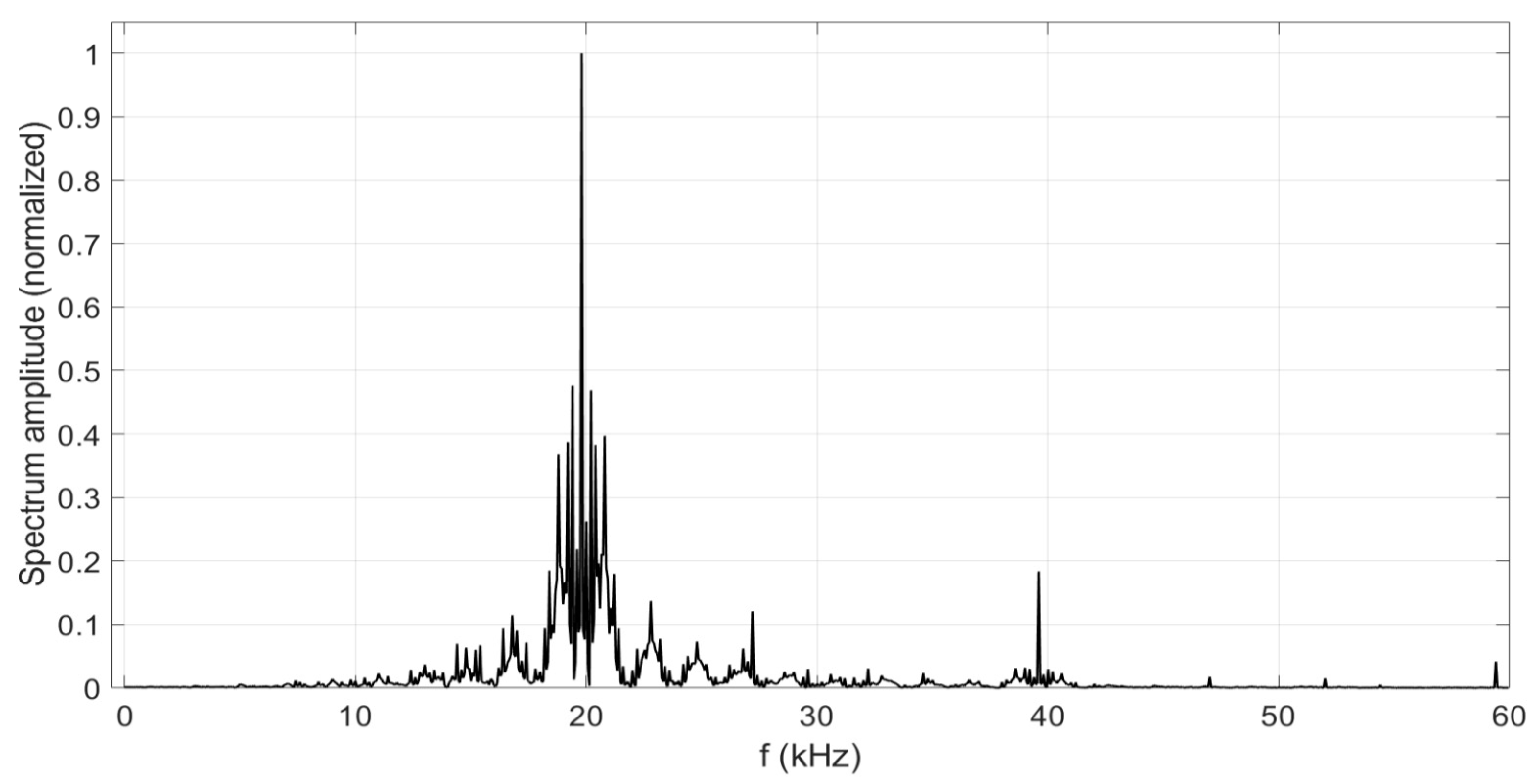
5.3. Results
5.4. Discussion
6. Conclusions
Author Contributions
Funding
Acknowledgments
Conflicts of Interest
References
- Honda, J.; Adams, J. Class D Audio Amplifier Basics, Application Note AN-1071. International Rectifier (USA), February 2005. Available online: https://www.infineon.com/dgdl/an-1071.pdf (accessed on 20 July 2020).
- Xu, D.; Zhou, G.; Huang, R.; Liu, X.; Liu, F. High Efficiency Half Bridge Class-D Audio Amplifier System with Front-end Symmetric Bipolar Outputs LLC Converter. In IEEE Transactions on Industrial Electronics; IEEE: Piscataway, NJ, USA, 2020. [Google Scholar]
- Auer, M.; Karaca, T. A Class-D Amplifier with Digital PWM and Digital Loop-Filter using a Mixed-Signal Feedback Loop. In Proceedings of the ESSCIRC 2019-IEEE 45th European Solid State Circuits Conference (ESSCIRC), Krakow, Poland, 23–26 September 2020; pp. 153–156. [Google Scholar] [CrossRef]
- Kuo, C.-H.; Liou, Y.-J. A Delta-Sigma Modulator with UPWM Quantizer for Digital Audio Class-D Amplifier. In Proceedings of the 2019 MIXDES-26th International Conference “Mixed Design of Integrated Circuits and Systems”, Rzeszow, Poland, 27–29 June 2020; pp. 293–297. [Google Scholar] [CrossRef]
- Li, Y.; Duan, F.; Jiang, J.; Wang, X. High-efficiency and low-consumption underwater sonar transmitter with improved triple-pulse HP-PWM signal model based on class D amplifier. EURASIP J. Wirel. Commun. Netw. 2016. [Google Scholar] [CrossRef] [Green Version]
- Galić, J.; Pešić-Brdjanin, T.; Iriškić, L. Class-D Audio Amplifier using Pulse Width Modulation. In Proceedings of the 6th Small Systems Simulation Symposium 2016, Nis, Serbia, 12–14 February 2016; pp. 133–136. [Google Scholar]
- Kovačević, S.; Pešić-Brdjanin, T.; Galić, J. Class D Audio Amplifier with Reduced Distortion. In Proceedings of the 2018 International Symposium on Industrial Electronics (INDEL), Banja Luka, Bosnia, Herzegovina, 1–3 November 2018; pp. 1–4. [Google Scholar] [CrossRef]
- Caldwell, J. Analog Pulse Width Modulation, TI Precision Designs: Verified Design (Texas Instruments Application Recommendations). June 2013. Available online: http://www.ti.com/lit/ug/slau508/slau508.pdf (accessed on 20 July 2020).
- Song, Z.; Sarwate, D.V. The frequency spectrum of pulse width modulated signals. Signal Process. 2003, 83, 2227–2258. [Google Scholar] [CrossRef]
- Crilly, P.B.; Carlson, A.B. Communication Systems, 5th ed.; McGraw-Hill Education: New York, NY, USA, 2009. [Google Scholar]
- Proakis, J.G.; Salehi, M.; Bauch, G. Contemporary Communication Systems Using MATLAB; Nelson Education: Toronto, ON, Canada, 2012. [Google Scholar]
- Mitola, J. Software Radio: Object-Oriented Approaches to Wireless Systems Engineering; John Wiley & Sons: Hoboken, NJ, USA, 2000. [Google Scholar]
- Grayver, E. Implementing Software Defined Radio; Springer Science & Business Media: Berlin/Heidelberg, Germany, 2012. [Google Scholar]
- Texas Instruments Mixed-Signal Products, “FSK Modulation and Demodulation with the MSP430 Microcontroller”, 1998. Application Report SLAA037. Texas Instruments. Available online: http://www.ti.com/lit/an/slaa037/slaa037.pdf (accessed on 20 July 2020).
- Pascual, C.; Song, Z.; Krein, P.T.; Sarwate, D.V.; Midya, P.; Roeckner, W.J. High-fidelity PWM inverter for digital audio amplification: Spectral analysis, real-time DSP implementation, and results. In IEEE Transactions on Power Electronics; IEEE: Piscataway, NJ, USA, 2003; Volume 18, pp. 473–485. [Google Scholar] [CrossRef]
- Koutroulis, E.; Dollas, A.; Kalaitzakis, K. High-frequency pulse width modulation implementation using FPGA and CPLD ICs. J. Syst. Archit. 2006, 52, 332–344. [Google Scholar] [CrossRef]
- Nguyen, K.C.; Sarwate, D.V. Up-sampling and natural sample value computation for digital pulse width modulators. In Proceedings of the 2006 40th Annual Conference on Information Sciences and Systems, Princeton, NJ, USA, 22–24 March 2006; pp. 1096–1101. [Google Scholar] [CrossRef] [Green Version]
- National Instruments Multisim. Available online: https://www.ni.com/en-lb/support/downloads/software-products/download.multisim.html#312060 (accessed on 20 July 2020).


| Parameter | [3] | [4] | [5] | [6] | [7] | This Work |
|---|---|---|---|---|---|---|
| Input signal type | Digital | Analog | Analog | Analog | Analog | Digital |
| Input signal voltage (V) | - | - | - | 1 | 1 | 1 |
| Input signal frequency (kHz) | - | 1 | - | 1, 5 | 1 | 2 |
| Switching frequency (kHz) | 390 | 384 | 200 | 300–800 | 500–2000 | 19.8 |
| Class-D amplifier modulation | PWM | UPWM | PWM | PWM | PDM | PWM |
| Filter type | Digital | - | LPF | LPF | LPF | BPF |
| Output type | Amplified | Amplified | Amplified | Amplified | Amplified | Amplified PSK |
| Output power (W) | 1.2 | - | - | - | - | 6 |
© 2020 by the authors. Licensee MDPI, Basel, Switzerland. This article is an open access article distributed under the terms and conditions of the Creative Commons Attribution (CC BY) license (http://creativecommons.org/licenses/by/4.0/).
Share and Cite
Zia, M.Y.I.; Tierno, R.; Luque-Nieto, M.-Á.; Otero, P. An Energy-Efficient Integration of a Digital Modulator and a Class-D Amplifier. Electronics 2020, 9, 1319. https://doi.org/10.3390/electronics9081319
Zia MYI, Tierno R, Luque-Nieto M-Á, Otero P. An Energy-Efficient Integration of a Digital Modulator and a Class-D Amplifier. Electronics. 2020; 9(8):1319. https://doi.org/10.3390/electronics9081319
Chicago/Turabian StyleZia, Muhammad Yousuf Irfan, Raúl Tierno, Miguel-Ángel Luque-Nieto, and Pablo Otero. 2020. "An Energy-Efficient Integration of a Digital Modulator and a Class-D Amplifier" Electronics 9, no. 8: 1319. https://doi.org/10.3390/electronics9081319