Article

Compact Wideband MIMO Diversity Antenna for Mobile Applications Using Multi-Layered Structure

1
Faculty of Arts, Science and Technology, Glyndwr University, Wrexham LL11 2AW, UK
2
School of Engineering and the Built Environment, Edinburgh Napier University, Edinburgh EH10 5DT, Scotland, UK
3
Faculty of Engineering & Informatics, University of Bradford, Bradford BD7 1DP, UK
4
Department of Electrical and Electronics Engineering, Khalifa University, Abu Dhabi P.O. Box 573, UAE
5
James Watt School of Engineering, University of Glasgow, Glasgow G12 8QQ, Scotland, UK
6
Department of Communication and Informatics Engineering, Basra University College of Science and Technology, Basra 61004, Iraq
*
Authors to whom correspondence should be addressed.
Electronics 2020, 9(8), 1307; https://doi.org/10.3390/electronics9081307
Submission received: 26 July 2020 / Revised: 8 August 2020 / Accepted: 12 August 2020 / Published: 14 August 2020
(This article belongs to the Special Issue Design and Theoretical Study of New Antennas)

Abstract

:
A closely packed wideband multiple-input multiple-output (MIMO)/diversity antenna (of two ports) with a small size of less than 18.5 mm by 18.5 mm is proposed for mobile communication applications. The antenna can be orthogonally configured for corner installation or by placing it on a back-to-back structure for compact modules. To enhance the isolation and widen the bandwidth, the antenna is structured with multiple layers having differing dielectric constants. The feeding through a via significantly reduces the ground waves. A multi-fidelity surrogate model-assisted design exploration method is employed to obtain the optimized antenna geometric parameters efficiently. The antenna design was investigated using electromagnetic simulation and a physical realization of the optimal design was then created and subjected to a range of tests. The specific parameters investigated included reflection coefficients, mutual coupling between the input ports, radiation patterns, efficiency and parameters specific to MIMO behavior: envelope correlation coefficient and pattern diversity multiplexing coefficient. It was found that the antenna has an impedance bandwidth of approximately 4 GHz, mutual coupling between input ports of better than −18 dB and an envelope correlation coefficient of less than 0.002 across the operating band. This makes it a good candidate design for many mobile MIMO applications.

1. Introduction

Small size, high data rates, reliable connectivity, and flexible operation without reconfiguration in many regions and systems are extremely attractive features in current and future mobile devices [1,2]. To achieve the above, wideband and higher-frequency antennas have experienced many developments in recent years [3]. Although this offers large bandwidth and high data rates, the high bandwidth makes the system more susceptible to multipath fading due to reflection and diffraction in a rich scattering environment [4]. To overcome this technical issue, ultra-wideband (UWB) wireless communication systems were proposed due to its attractive features such as excellent immunity to multipath interference and high data rates [5,6]. Multiple-input multiple-output (MIMO) technology is another effective technique for mitigating this issue, in addition to its features of increasing the channel capacity and transmission quality [4]. By combining both UWB and MIMO technologies, a new MIMO-UWB system can further alleviate the multipath issue [7]. However, due to some existing wireless standards, i.e., WiMAX (3.3–3.7 GHz), WLAN (5.15–5.35 GHz, and 5.725–5.825), etc., that share the frequency bands within the UWB regulation standards, this causes interference to the UWB system and degrades its performance. To suppress these unwanted interferences, band-rejected UWB antennas have been studied widely and intensively [8]. Due to the above design technical challenges, the design of the wideband antenna is deemed to be a challenge in meeting the compact size and high bandwidth requirements of many MIMO-orientated applications [7].
Constraining mutual coupling in a narrow-band antenna is relatively straightforward, but the greatly increased degrees of freedom in a wideband one makes it very challenging in such a case, especially if size is also constrained. A number of past studies have attempted to address this problem, with varying degrees of success [9,10,11,12,13,14,15,16,17,18,19,20,21,22,23,24,25]. In [9,10,11,12,13,14,15,16,17,18], various decoupling structures were suggested to be interposed between several symmetrically placed elements to enhance isolation between them. These methods are using Electromagnetic Band Gap structure [9], adopting distinct patterns and polarization of the radiator [10,11,14], defected or modified ground plane [12,16,17], neutralization strip [13,20], embedded periphery slot [22], parasitic stubs [15,18] and metamaterial [19,21]. In [23,24,25,26], differently structured antenna elements were combined to achieve pattern diversity. However, low correlation coefficients could be achieved because of diverse radiation patterns and polarizations. In [27,28,29,30], different feeding techniques were implemented to attain MIMO features. By optimizing the feeding, radiator and ground structures, works in [31,32] managed to suppress the mutual coupling while maintaining a reasonable size.
The basic microstrip patch antenna is strongly resonant as the dielectric space beneath can be regarded as a cavity resonator. The bandwidth is thus narrow, but much ingenuity has been expended over the years to soften the resonance by choosing elaborate patch shapes, deepening the substrate dielectric, reducing substrate permittivity or even increasing loss [33]. In addition, higher-order impedance matching and design of the structure to have multiple resonances have been found to be useful tools to improve the bandwidth. Another technique to improve bandwidth is to use multiple loosely-coupled patches and bandwidth can be further improved by driving them parasitically in a stacked structure. While vertical stacking of patches is a known broadbanding technique, large bandwidth is achieved here by feeding the driven (main) patch through a via and the use of parasitic patches that are laterally displaced in a single plane. This lateral displacement with respect to the center of the main patch, generates multiple odd-order resonances which cause the bandwidth to increase significantly [34].
The computationally expensive full-wave electromagnetic (EM) simulations results in standard global optimization techniques taking a very long time, expected to be approximately 1.5 months, to find a highly optimal design. To address this challenge, a state-of-the-art approach, the surrogate model-assisted differential evolution algorithm for antenna synthesis (SADEA) [35], was employed in many antenna designs. By using an Intel Core i7-4770k computer, the optimization time could be reduced to only 20 h in a high-fidelity full-wave EM simulation antenna model.
By combining all the available design concepts for mutual coupling reduction [9,10,11,12,13,14,15,16,17,18,19,20,21,22,23,24,25,26,27,28,29], bandwidth-enhanced methods [33,34] and a computationally efficient optimization method [35], this paper presents a stacked wideband MIMO antenna to cover a 4.5 to 8.5 GHz band for mobile application. The design implemented high dielectric constant substrates, modified the shapes of the parasitic patches and radiator, and a feeding structure to obtain the required characteristics of compact size, good return loss, low mutual coupling level and reasonable gains and radiation patterns.
The structure of this paper can be summarized as follows. In Section 2, the details of the antenna geometry and operating principles are given. The optimization method used in our design and the parameter studies of the proposed work are discussed in Section 3. The experimental setups are described and results are compared with simulated results in Section 4. Finally, conclusions are drawn in Section 5.

2. Antenna Configuration, Feeding Structure and Design Concepts

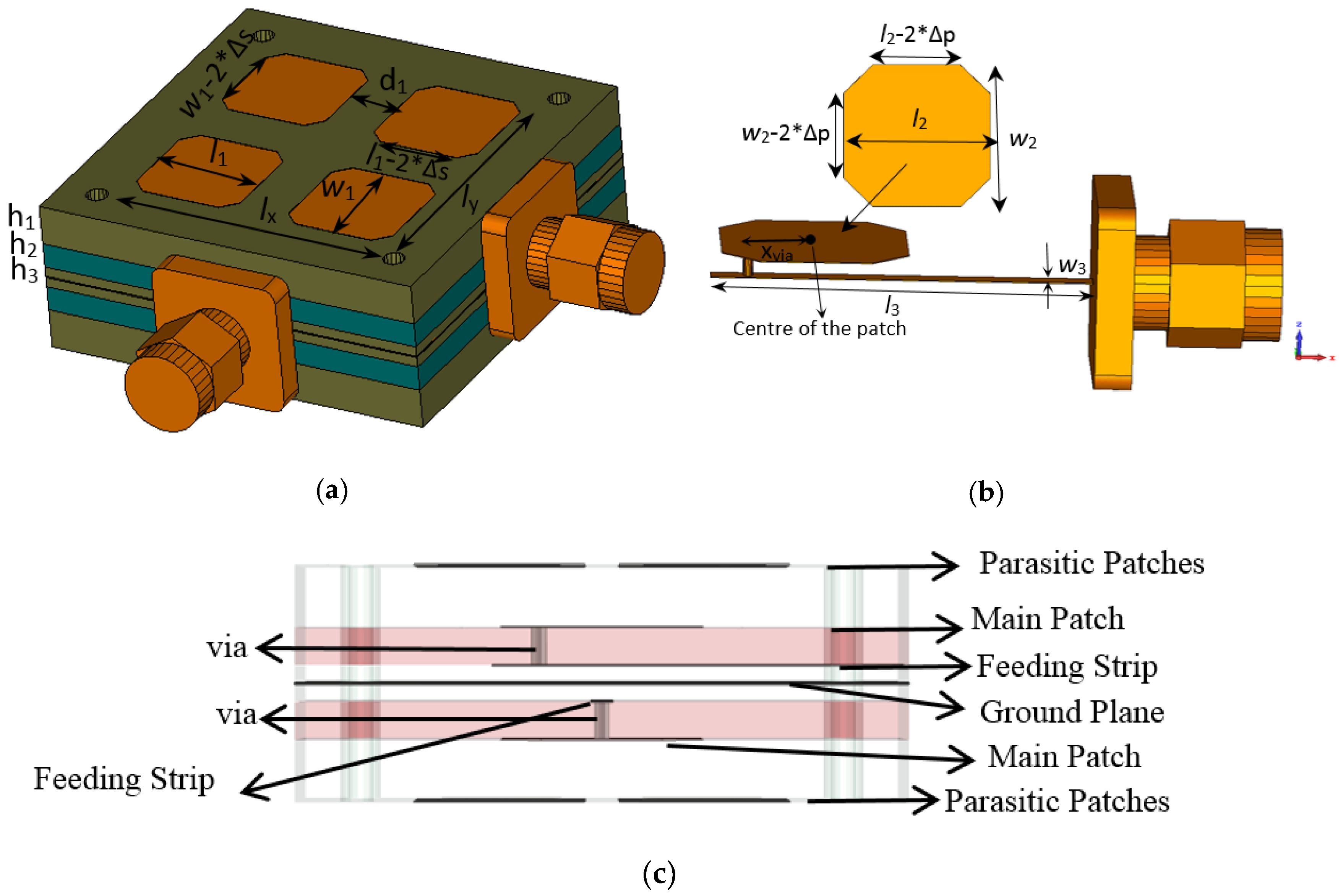
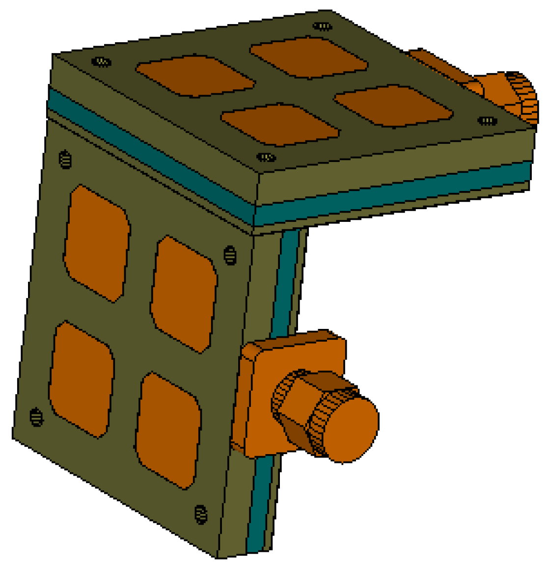
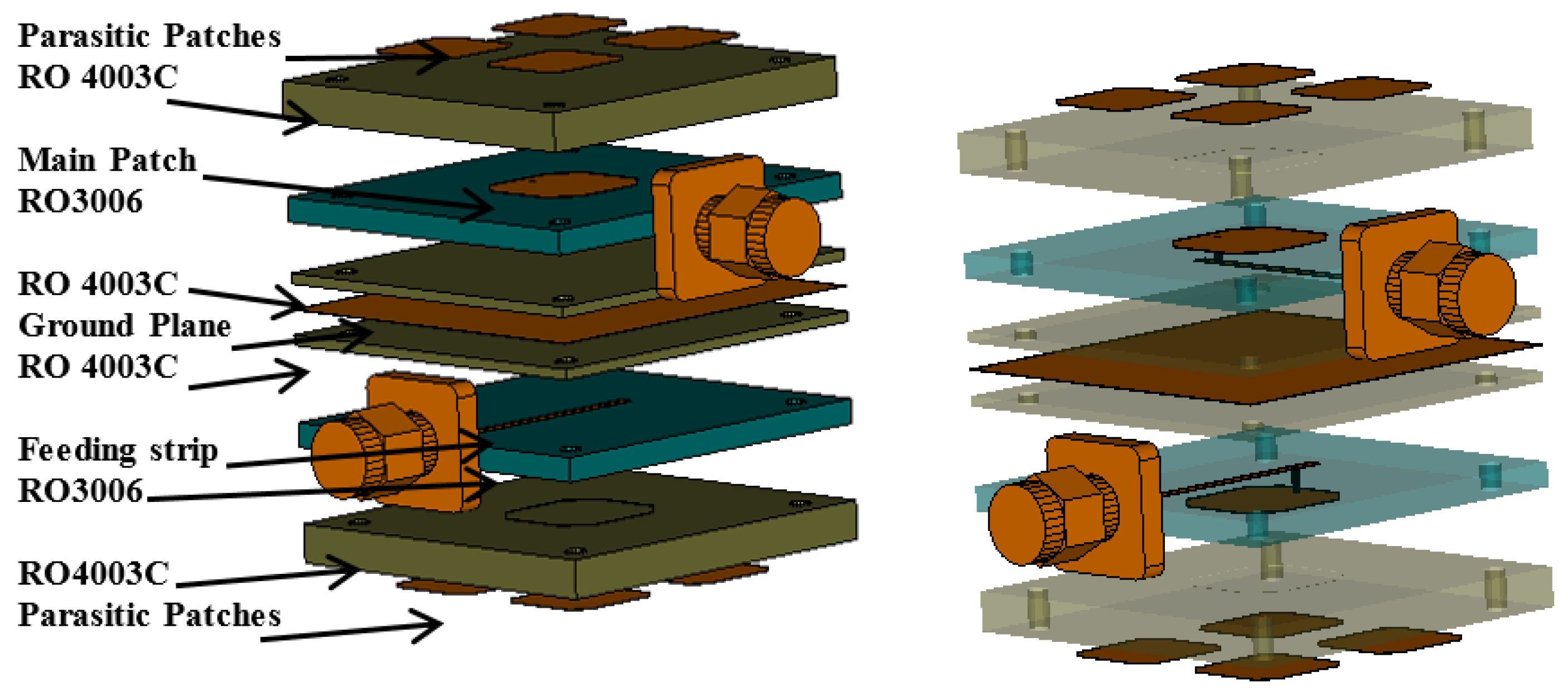
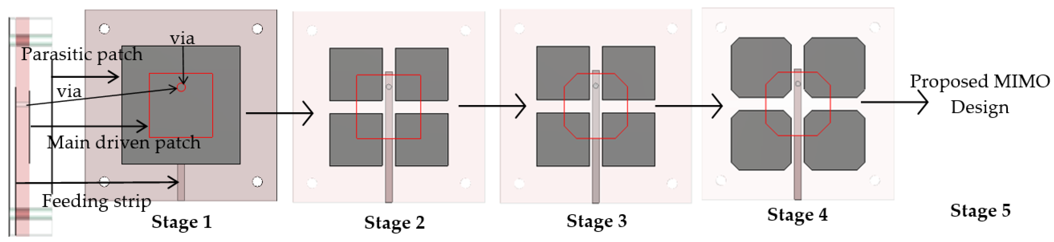
2.1. Antenna Geometry and Design Concepts

The original idea of this antenna design was from [34]. This work used four rectangular patches on the top layers of the first low-permittivity substrate and a T-shaped patch with a full ground to feed the antenna on the second identical substrate. By stacking the both substrates, an impedance bandwidth of 29% across the frequency from 3.5 to 4.7 GHz was achieved [34]. To enhance the performance of this previous design and also introduce the MIMO characteristics into the design, the proposed stacked wideband MIMO antenna array has the dimensions 30 × 30 × 10 mm (W × L × H), with two feeding ports proposed, as illustrated in Figure 1a. The actual dimensions of the structure could be made much smaller, down to 18.5 × 18.5 × 10 mm (lx × ly × H), but the extra area was needed in order to fasten together the various substrates with screws.
The design steps of this proposed antenna can be summarized as follows. Firstly, to implement the multiple patch design, an array of four parasitically-driven elements was used, separated by a dielectric layer from the driven element. The driven element has an initial dimension of 13 × 13 (l2 × w2) mm2, where 13 mm is equivalent to 0.5 λ at 4.5 GHz, which is the lowest operating frequency, while the parasitic patches have calculated dimension of 9.6 × 9.6 (l1 × w1) mm2, where 9.6 mm is equivalent to 0.5 λ at 8.5 GHz, which is the highest working frequency. In this case, the driven element controls the lowest resonant frequency, while the parasitic patches govern the highest resonant frequency. By carefully merging these two resonance frequencies, wide impedance bandwidth can be achieved. Secondly, it is crucial to select the right thickness of each layer of the structure in order to achieve the required good impedance matching level and acceptable radiation characteristics. In layer 1, the dielectric was 3.048 mm in thickness (h1), with a permittivity εr1 of 3.38. The four parasitic patches with corner truncation have the dimensions 9.6 × 9.6 mm2 with a spacing gap d1 of 1.5 mm. With this thicker substrate, this ensures a lower Q value and, thus, broadening the antenna impedance bandwidth. Further, according to [35], the broadband response can be achieved by having the antenna substrate height between the parasitic patch and the driven patch as h1 < 0.1λ. Hence, h1 should not exceed this limit. The second layer (layer 2) has a εr2 of 6.15 and a thickness (h2) of 1.28 mm. This is different than the one in [34], where the same low-permittivity substrates were used for both layers. To feed the 13 × 13 mm3 of driven element, the main patch, a stripline of approximately 20 mm in length (l3), leading from an SubMiniature version A (SMA) connector, is placed on a third substrate (layer 3) below the dielectric layer supporting the driven element. This layer has the same permittivity as layer 1 but is somewhat thinner (h3 = 0.813 mm). It should be noted that the following formula was used to determine the maximum allowable height for all the thicknesses of the design to avoid surface wave loss, where h is height and εr is the dielectric constant of the substrate [36]. By carefully selecting the height for each substrate by adopting this formula, the surface wave loss is negligible.
h λ < 0.3 2 π ε r
Thirdly, the strip runs underneath the driven element and is then connected to it by a conducting via traversing layer 2, as shown in Figure 1b,c. The impedance at the feed point of a rectangular microstrip patch depends on the distance of this point from the edge of the patch and thus the use of a feed by a via connection from beneath allows precise adjustment of this parameter. This is more complex and costly than approaches using a feed line and patch on the same plane, but it enables optimal tuning of the impedance and tends to facilitate wider impedance bandwidth and improved purity of polarization. The section of stripline between the via and the input-side patch edge forms, together with the lower patch surface, a stub line that is short circuited by the via. The stub’s reactive input impedance is equivalent to a series reactive matching element connecting the stripline to the patch edge.
Finally, two copies of this complete subarray structure were then created and placed back to back, but rotated 90° with respect to each other. A central copper ground plane separates the two copies of the structure. Excited at its two ports, the structure produces two pattern functions which prove to be nearly uncorrelated (i.e., mathematically orthogonal) and are suitable for diversity or MIMO use. These patterns can be considered to exhibit a mixture of pattern shape and polarization diversity. A second uncorrelated pattern can also be produced in other ways, for example the ”orthogonal” configuration shown in Figure 2.
The complete assembly of the two subarray elements with their feeding structure is shown in exploded form in Figure 3. The structure of the feed from the SMA connectors to the respective driven patches is as shown in Figure 1b (where the dielectric is rendered transparent), this structure being chosen to enable widening of the operational bandwidth while leaving the radiation pattern largely unaffected. The stacked structure also permits adjustment of the radiation pattern through modification of the layout of the parasitic patches without the need for alteration of the feed structure. The dielectric between the feed line and the driven patch was chosen to be a 1.28 mm in thickness Rogers Corporation high frequency laminate of type RO3006. The layer beneath the feeding strip was chosen to be a Rogers Corporation 4003C, with a thickness of 0.813 mm.
The optimal design parameters given in Table 1 were arrived at after the application of the design optimization procedure presented in the following Section 3. The procedure was given the freedom to adjust the dimensions of the top patches, their separations and the thicknesses of the dielectrics in layers 1 and 2. However, it should be noted that the choice of dielectric thickness is severely constrained by the values available on the market.
To understand the basic operational principles of this antenna, the evolution process of the design has been divided into five stages, as illustrated in Figure 4. This will help to simplify the analysis of the contribution of each part of the antenna in terms of impedance bandwidth and matching, and gain over the intended wideband operating frequency band (4.5 to 8.5 GHz), as shown in Figure 5. In Stage 1, the antenna consists of a large top parasitic patch and it is excited by a driven patch below it. In this configuration, two resonant frequencies, i.e., 3.1 GHz and 5.8 GHz, can be attained in the S11 plot, as illustrated in Figure 5a. The first resonant frequency is controlled by the length of the parasitic patch (18.5 mm, equivalent to 0.35 λ at 3.1 GHz) while the second resonant frequency is governed by the length of the driven patch (10 mm, equivalent to 0.5 λ at 5.8 GHz). By dividing a single parasitic patch into four patches with each has size of 8.5 mm × 8.5 mm, as depicted in Stage 2 of Figure 4. These four radiating patches on the top of each subarray are parasitically excited through an electromagnetic coupling area located at one of their corners which overlaps with the driven patch below them. This combination structure enables wide bandwidth with acceptable S11 (better than −8 dB) and good gain (above 5 dBi), as shown in Figure 5a,b. To further improve the matching of the antenna, the four corners of the main driven patch are truncated, as shown in Stage 3 of Figure 4. As can be observed in Figure 5a,b, the S11 is now well below −10 dB and the gain of the antenna also shows an increment of approximately 0.2 to 0.4 dBi across the desired operating frequency band. In Stage 4, the four corners of the four parasitic patches are truncated. By changing this, the S11 stays at a similar level while variation in the gain has been minimized, as shown in Figure 5. To form the proposed MIMO antenna in Stage 5, two copies of the same antenna in Stage 4 are placed back to back, but are rotated 90° with respect to each other, as depicted in Figure 1 and Figure 3. With this modification, no significant change of the performance can be noticed in Figure 5.

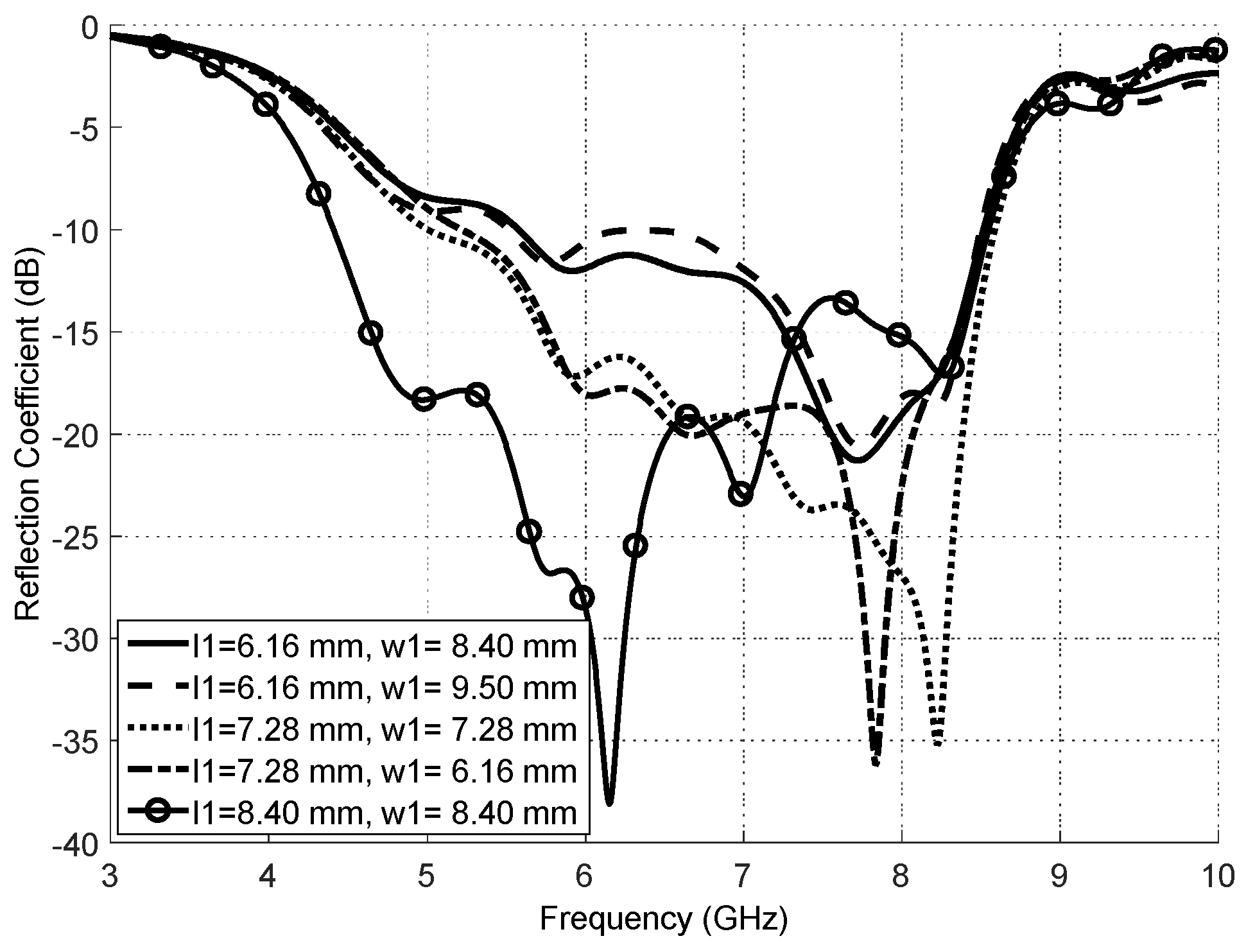
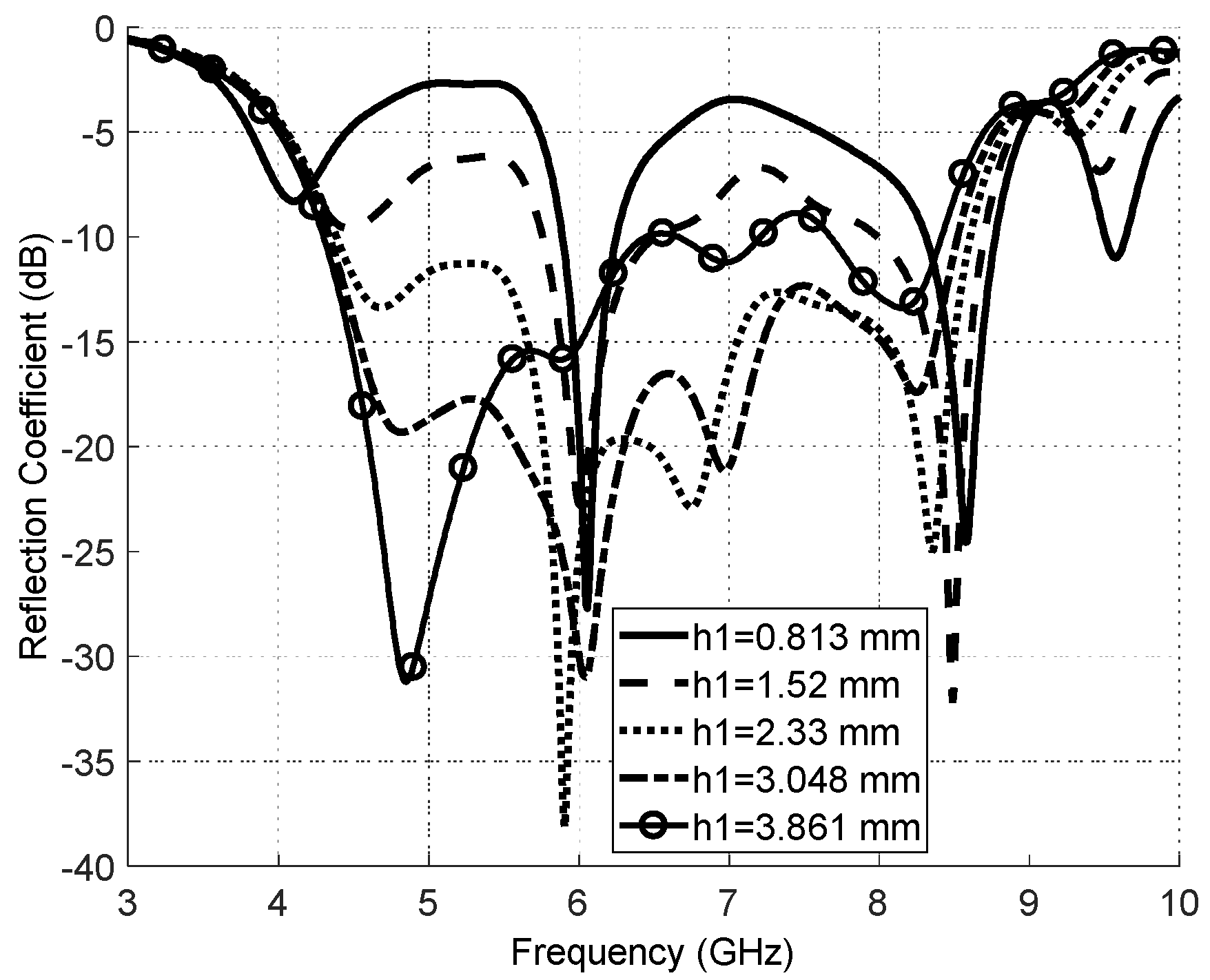
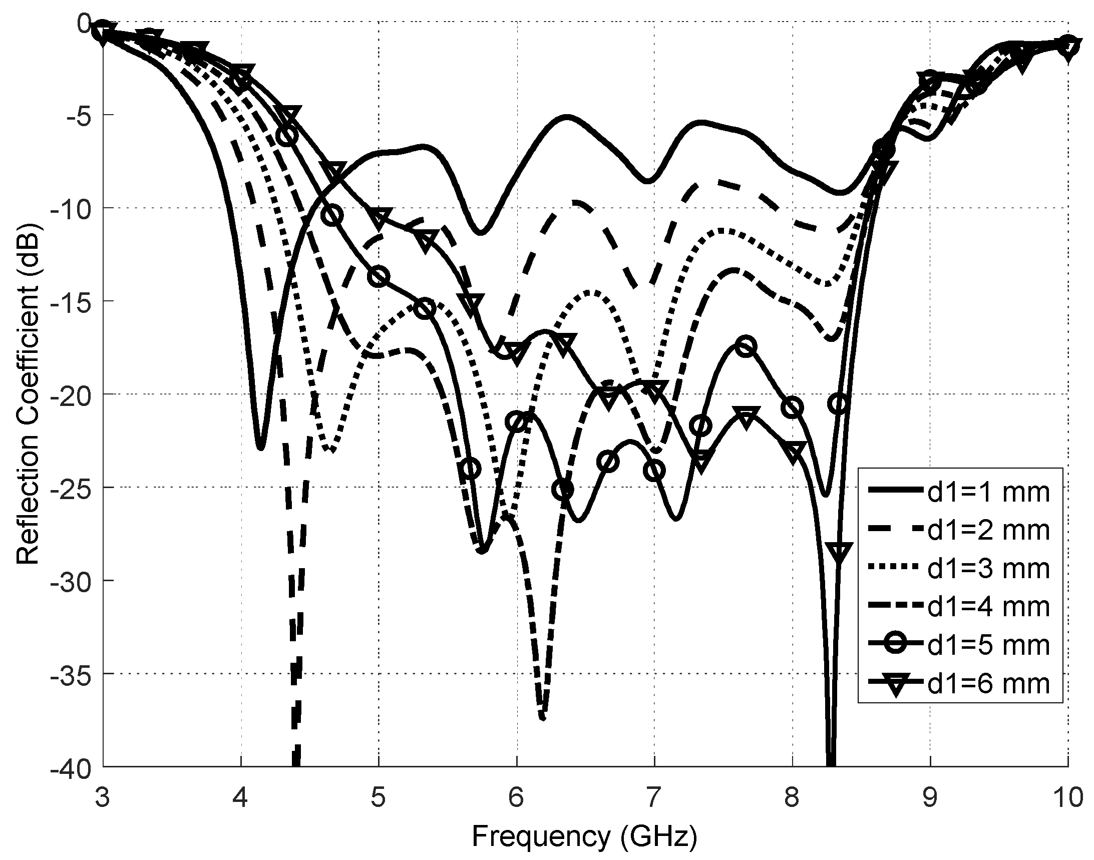
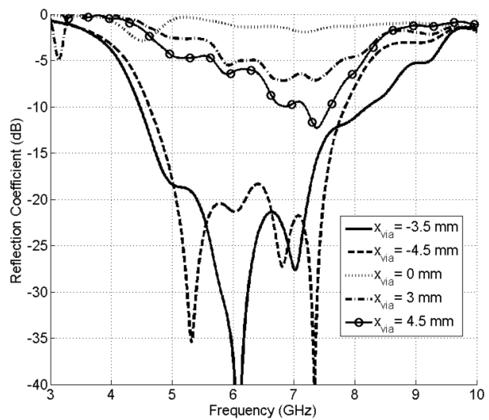
2.2. Antenna Geometry Parametric Study

When undertaking optimization of the radiation performance and impedance matching of the subarray, the focus must be on the principal parameters of the design: the dimensions of the radiating patches, their separations, the thickness h1 of the top layer (layer 1) and the location of the via connection feeding the driven patch. The process to find the optimum values of these principal parameters was undertaken using the CST computational electromagnetics time-domain simulation software, by Dassault Systems. Using the parameter sweep function in this software, the patch and stripline geometries could be varied widely, enabling the feed-point S parameters to be evaluated, as explained below.
In the optimization process, the length l1 and width w1 of the radiating patches were varied simultaneously from 5 to 10 mm, with d1 = 1.68 mm, h1 = 3.048 mm and xvia = −3.5 mm (see Table 1). Examining the results, as displayed in Figure 6, it is seen that an increase in the size of the radiating patches causes the excitation of an upper resonance, occurring above 8.48 GHz. Increasing the size further causes the lower resonance (approximately 4.45 GHz) to disappear. Further, the results for the S11 parameter show that these two resonances are strongly excited when l1 = w1 = 8.4 mm.
Pursuing another controllable parameter, alternative values of the thickness of layer 1 (h1) were considered. Only values that are commercially available can realistically be considered, since custom values would be prohibitively expensive. The standard thicknesses that are available for Rogers Corp. laminate of type RO4003C are 0.813, 1.52, 2.33 (two layers of 1.52 mm and 0.813 mm bonded together), 3.048 (two layers, both of 1.52 mm, bonded together) and 3.861 mm (three layers, of 1.52, 1.52 and 0.813 mm). The effects of these options were modeled in the CST software and the results for S11 are shown in Figure 7. It is observed that, for the thinnest case (h1 = 0.813 mm), the lower resonance (approximately 5 GHz) disappears and the higher one (approximately 7 GHz) is relatively weak. However, with the increase in substrate height, the two principal resonances become increasingly stronger until they fade again at the maximum height studied (3.861 mm). It is thus seen that the optimum choice is the next-highest value, 3.048 mm, which provides values of S11 better than −10 dB over the 5–7.5 GHz band, bracketed by two strong resonances.
Variation in the space separating the parasitic elements (d1) was investigated next. This was varied over the range from 1.00 to 6.00 mm, while the other parameters were held at the optimum values that had been previously determined. The results of this investigation are shown in Figure 8, where it is observed that the bandwidth between the upper and lower resonances decreases as this spacing is increased. However, with the narrowest spacing (1.00 mm), the value of S11 over the intervening range of frequencies rises above −10 dB and hence is not acceptable for mobile applications. When d1 equals to 2 or 3 mm, an optimum situation is found, with sharp upper and lower resonances at an adequately wide separation, and S11 values across the intervening band that are acceptable for wideband operation. Beyond this value of d1, the bandwidth falls again and eventually the upper resonance becomes completely eliminated.
Finally, the placing of the via connecting the feeder stripline and the driven element was investigated (parameter xvia). Figure 9 shows the values of S11 that were found, for a range of values of xvia. The trivial case of xvia = 0 is included for comparison but this, predictably, produces non-viable results. The other values investigated were symmetrically distributed in the positive and negative directions, but the interaction with the stripline resulted in significantly differing results and the only value that gives acceptably low S11 over an adequate bandwidth is xvia = −3.5 mm.
The simulation results that have been presented illustrate the complexity of optimizing the proposed antenna structure. As mentioned above, standard global optimization techniques may cost a very long time (estimated 1.5 months for this particular case). To address this problem, a new antenna optimization method, called multi-fidelity surrogate model-assisted differential evolution algorithm for antenna synthesis (MSADEA) is introduced in the next section.

3. Design Exploration of the Wideband MIMO Antenna Units

3.1. Multi-fidelity Surrogate Model Assisted Differential Evolution Algorithm

MSADEA is composed of two stages, in which Stage 1 is the SADEA method [37] using a low-fidelity EM model. The search ranges of the design variables are large, covering all possibilities. The three key elements of SADEA include Gaussian process machine learning for surrogate modeling [38], differential evolution for evolutionary optimization [39] and the surrogate model-aware evolutionary search framework [40,41] to make surrogate modeling and evolutionary optimization work harmoniously for antenna design landscapes. The method uses a computationally cheap Gaussian process surrogate model to approximate the computationally expensive EM simulation model in order to reduce the number of necessary EM simulations in the optimization process. With the surrogate model-aware evolutionary search framework, SADEA has advantages in terms of optimization ability and efficiency compared to several other surrogate model-assisted optimization methods for antenna design exploration. More details are given in [37,42]. In addition to reducing the necessary number of EM simulations, a low-fidelity EM model is used to reduce the computational time of each simulation in this stage.
Stage 2 of MSADEA performs a local search using the best design obtained by Stage 1 as the starting point. A high-fidelity full-wave EM model is now used. Due to the limited accuracy of the low-fidelity EM model, the obtained best design from Stage 1 may reveal markedly degraded performance when analyzed with the high-fidelity EM model, but it is sufficient to serve as a starting point for the Stage 2. There are several possible alternatives for the local optimization, and among them, the derivative-free Nelder–Mead simplex method [43] is used.
The advantage of MSADEA compared to SADEA is the higher efficiency. To build a global surrogate model, SADEA still has to carry out a number of high-fidelity EM simulations in non-optimal regions of the design space. In contrast, MSADEA uses low-fidelity EM simulations to replace them and high-fidelity simulations are only used near the optimal region. Hence, the overall efficiency is further improved.

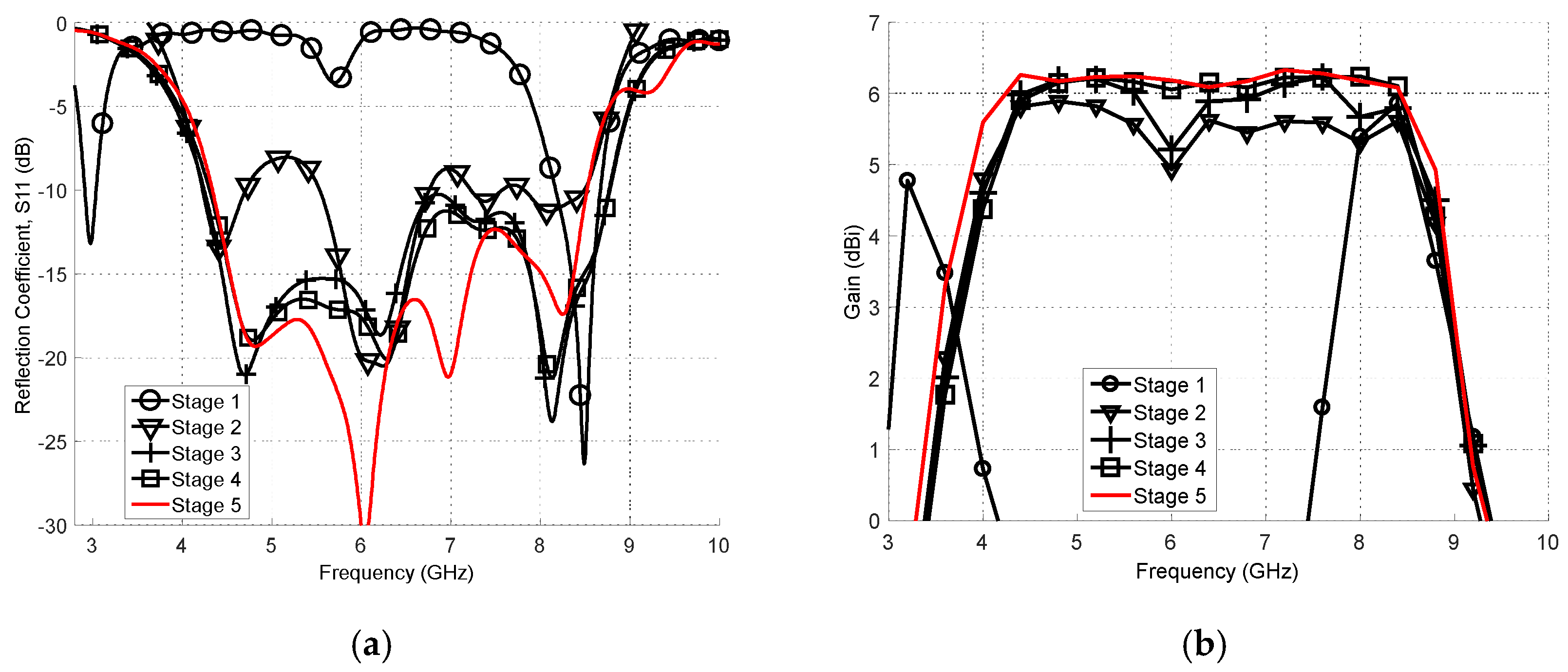
3.2. Implementation of MSADEA for the Wideband MIMO Antenna

The design variables of the wideband MIMO antenna include the length and width of the driven patch (l2 and w2) and the parasitic patches (l1 and w1), the separation between the parasitic elements d1, the location of the via with respect to the center of the radiating patch (xvia) and the length of the stripline (xport). Their ranges are shown in Table 2. The objective function minimizes the maximum of S11 and S21 in the operating band, as shown in (2)
Minimize max|S11|and |S21| (4.5 GHz–8.5 GHz)
The following geometric constraints have to be satisfied:
l1 + d1 0
d1 2 × min([15 − l1/2 5]) 0
l2/3 + abs(xvia) ≥ 0
Both the low- and high-fidelity EM models are built in CST Microwave Studio, using approximately 89,888 and 7,796,250 mesh cells, respectively. The corresponding simulation times are approximately 1.5 min and 12 min, respectively, using the PC mentioned earlier.
The SADEA method is implemented by the ADE tool [44] (ade.cadescenter.com). In ADE, all the algorithm parameters are automatically set. After 430 low-fidelity EM simulations (approximately 14 h), Stage 1 converged. The obtained best design is shown in Table 3. The max(|S11|) and max(|S21|) of the best design of Stage 1 is −10.31 dB and −22 dB, respectively, in terms of the low-fidelity EM model, but when using the high-fidelity EM model, the max(|S11|) is −8.12 dB and the max(|S21|) is −20.12 dB. Using this design as a starting point and after 32 high-fidelity EM simulations, the optimal results are max(|S11|) = −12.08 dB and max(|S21|) = −22.12 dB in the operating band, taking approximately 6 h. The final design obtained is shown in Table 3. The total design exploration time was 20 h.

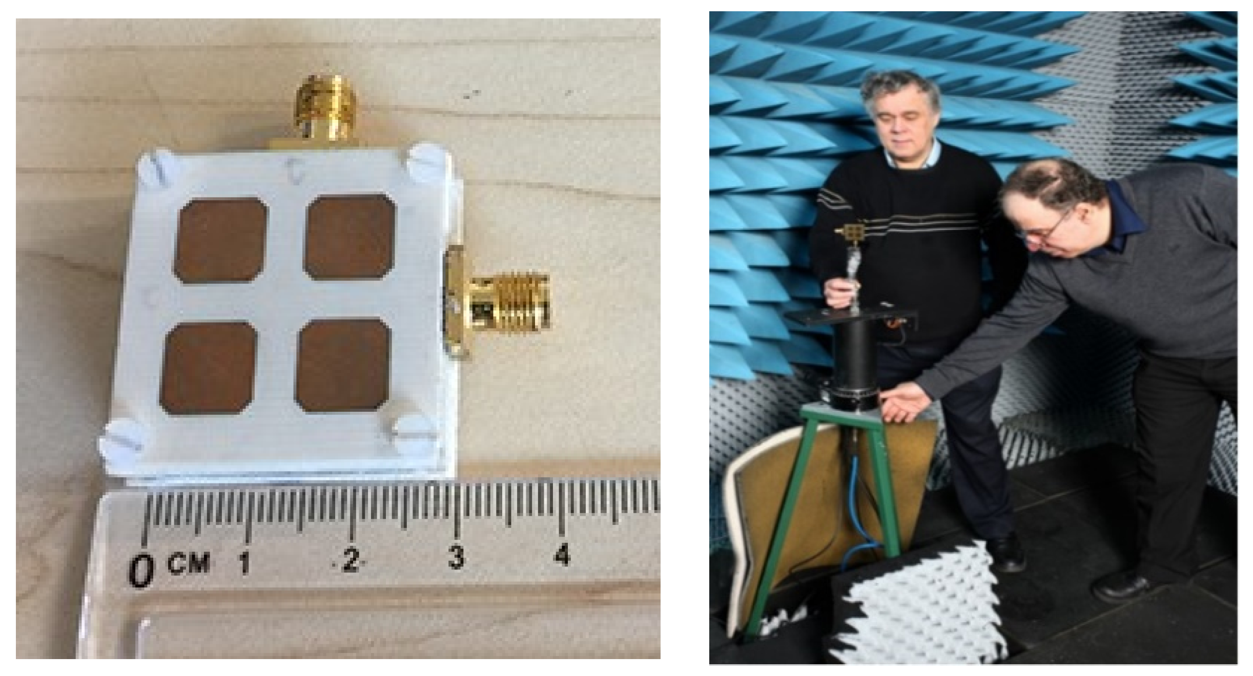
4. Measurement Results and MIMO Performance

The optimized candidate design shown in Figure 10 was created in physical form and subjected to a range of tests. A practical issue that arose was when the 4003C laminate with a thickness of 3.048 mm became unavailable and hence this had to be replaced by two layers, with a thickness of 1.52 mm, bonded by screws.
The results of the tests are given below, but it should be understood that some physical tolerances have to be allowed for, such as air gaps between the laminate layers, metallic unevenness in the soldering of the SMA connectors and the via connection, and test equipment tolerances.

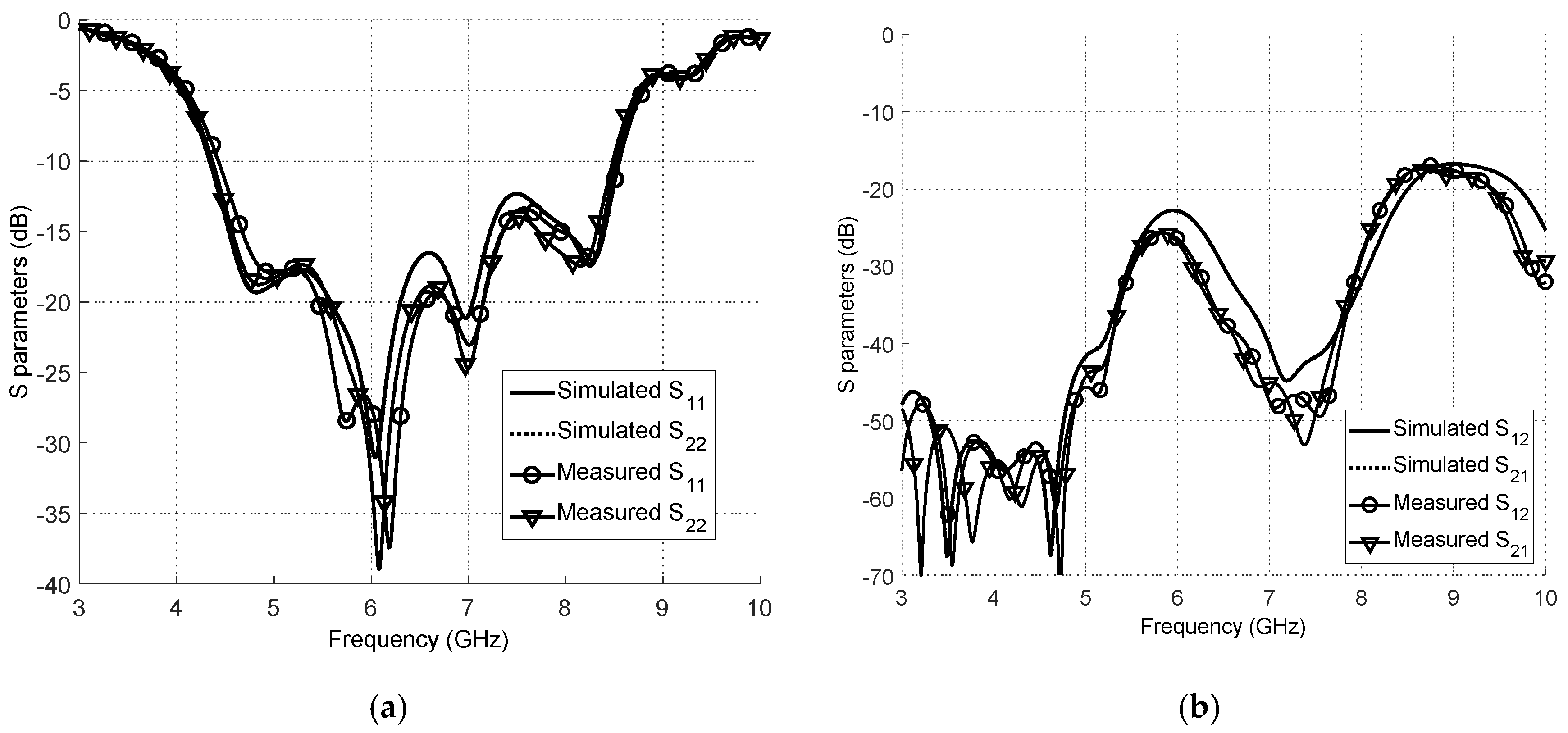
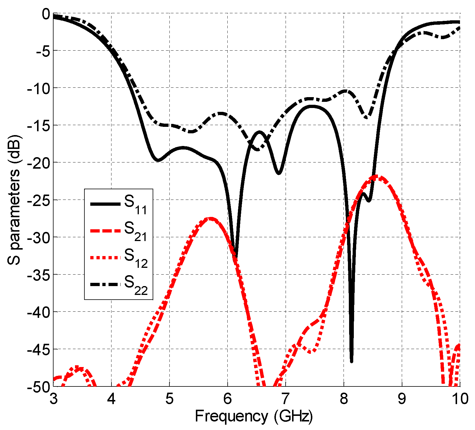
4.1. Reflection Coefficient (S11) and Impedance Bandwidth

Measurements of the input parameter S11 were compared with simulated values obtained from the time-domain solver in CST Microwave Studio software. The physical measurements were undertaken with a two ports vector network analyzer (VNA model: HP8720B). The input power of the VNA is set to 0 dBm in the measurement. S11 and S22 measurement was carried out by connecting one port of the antenna to the VNA, while the other port is terminated to a 50 ohm load. As for S21/S12 measurement, both ports of the antenna were connected to the corresponding two ports of the VNA.
A comparison of the measured and simulated results for S11 is given in Figure 11a, showing good agreement between the two sets of results, except in the deep resonance nulls, which can be explained by masking noise issues in the measurements and it can be also attributed to reflections from the SMA connectors and feed cable effects, and small inaccuracies in assembling the real structure that is fabricated using conductive epoxy adhesive. This shows that the antenna has a simulated S11 better than −10 dB over a range from 4.45 to 8.48 GHz, i.e., a bandwidth of slightly over 4 GHz, although the measured value is slightly less—4.53 to 8.19 GHz. This modest discrepancy can be explained by the considerations in the paragraph above.
The mutual coupling S parameters shown in Figure 11b are in close agreement with each other, but the measured and simulated values differ by a margin which averages approximately 8 dB. However, this disagreement is in favor of the measurements, which surprisingly show better performance than the simulation: the simulated values are below −18 dB across the desired band and the measured values below −30 dB, meaning that the device easily satisfies the requirement in the FCC Ultra-wideband standard of mutual coupling better than −15 dB [18].
Furthermore, the alternative orthogonal configuration shown in Figure 3 was also investigated and all four S parameters were measured. The results of Figure 12 were similar to those above: over the band 4.78–8.40 GHz (3.7 GHz bandwidth), S11 and S22 are better than −10 dB. The values of S12 and S21 are all better than −21 dB over the required bandwidth, which exceeds the performance of the published works [18,19,20].

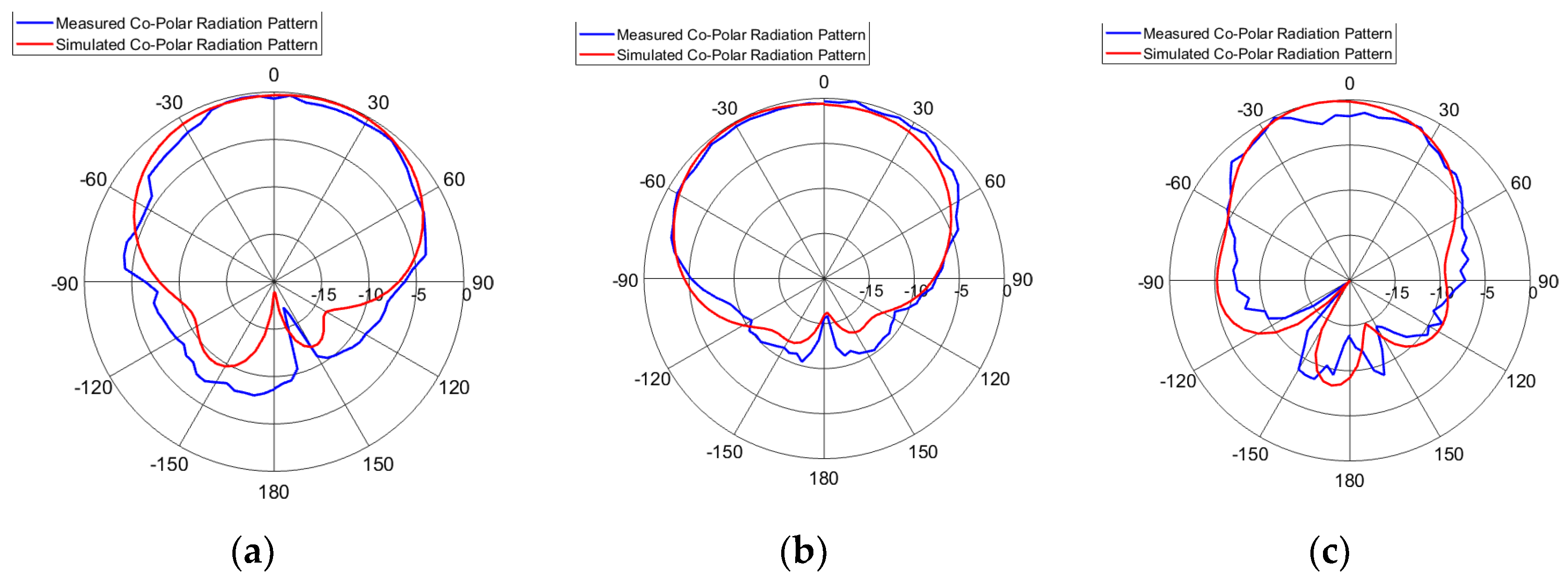
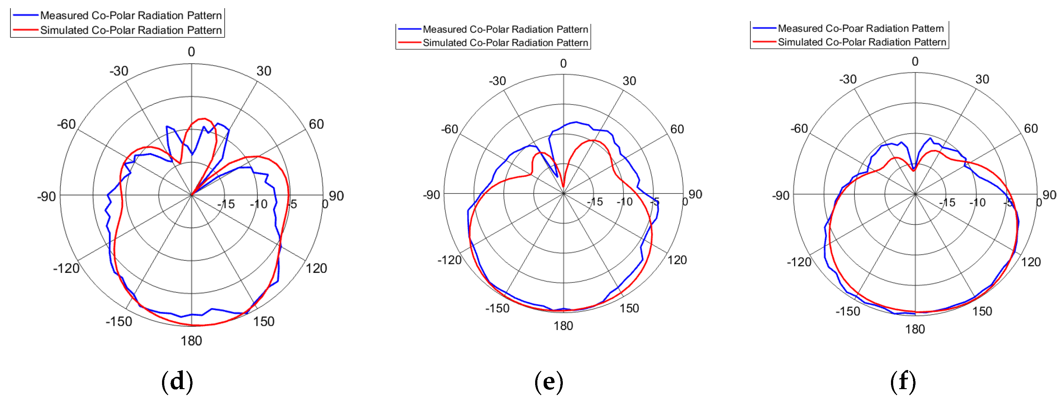
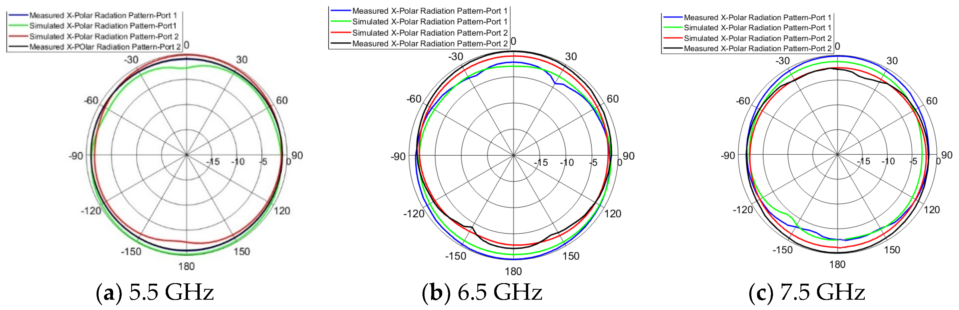
4.2. Radiation Patterns

Measurements of the far field radiation patterns of the prototype antenna were carried out in a 100 m3 anechoic chamber using an elevation-over-azimuth positioner, with the elevation axis coincident with polar axis ( θ =   0°) for the antenna’s co-ordinate system, as shown in Figure 10. The azimuth drive thus generated cuts at a constant . The fixed antenna (reference antenna) was a broadband horn (EMCO type 3115) positioned at 4 m. The elevation positioner was rotated from a θ of −180 to 180° in increments of 5° for the chosen measurement. Radiation patterns for both ports of the antenna design shown in Figure 1 were investigated by simulation and measurement at three representative frequencies: 5.5, 6.5 and 7.5 GHz. Simulations were again derived using CST Microwave Studio and the measurements were undertaken in an anechoic chamber. The principal (co-polar) results are shown in Figure 13 and show good agreement between simulation and measurement. Modest discrepancies in the measurement results can be ascribed to the supporting hardware in the anechoic chamber and gain error in the standard antenna used for the measurements. The slightly inconsistent radiation patterns were observed, but this is acceptable and insignificant for mobile application when this antenna is employed in a rich scattering environment.
The corresponding results for cross-polar patterns are shown in Figure 14. These are less than 15 dB lower than the co-polar patterns: the diagrams are re-normalized by adding 15 dB so that the 0 dB level is equivalent to 15 dB lower than the results in Figure 13. Cross-polar components are undesirable and can cause uncertainty in MIMO systems but −15 dB of suppression is adequate for many applications.

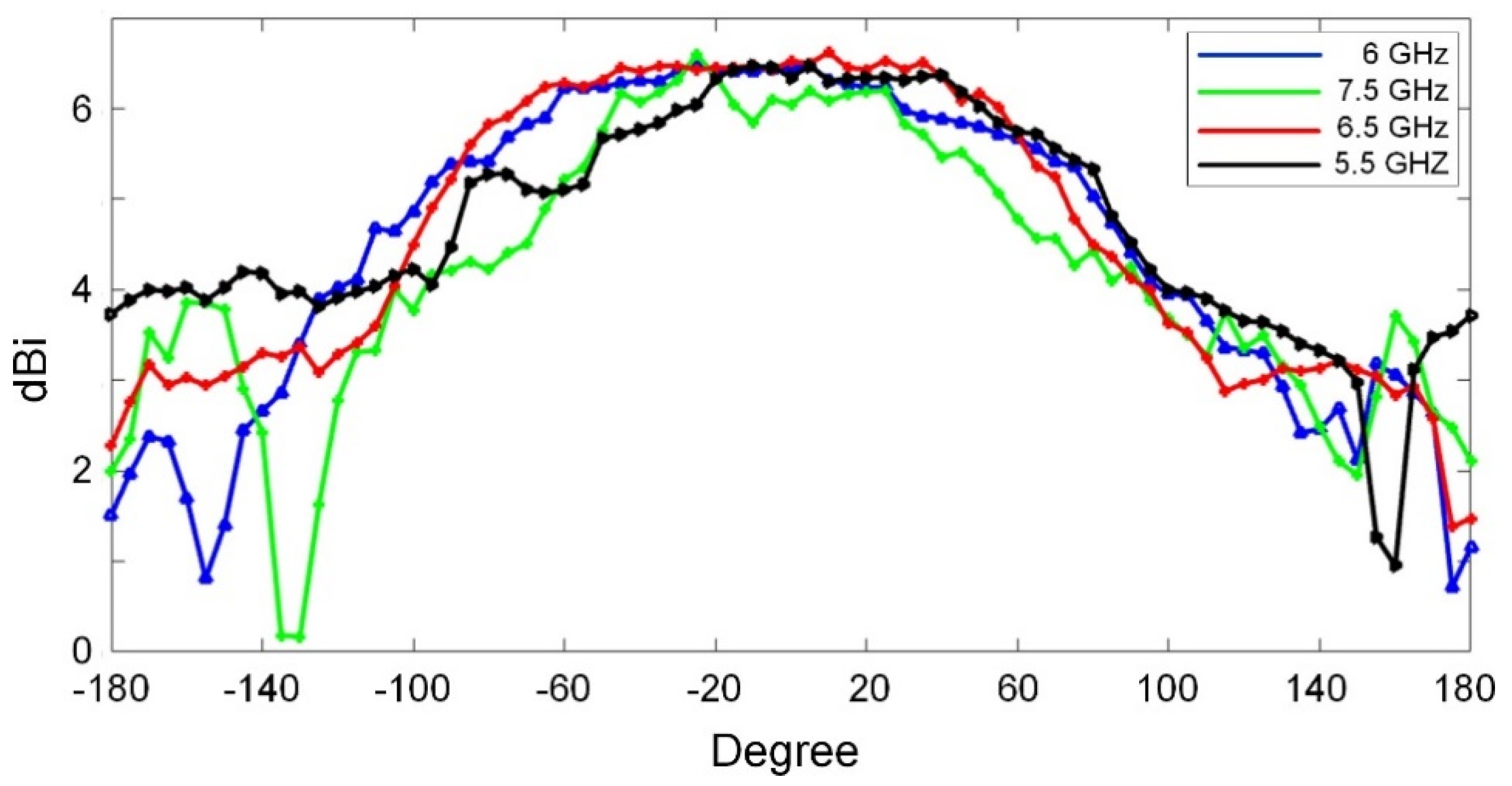
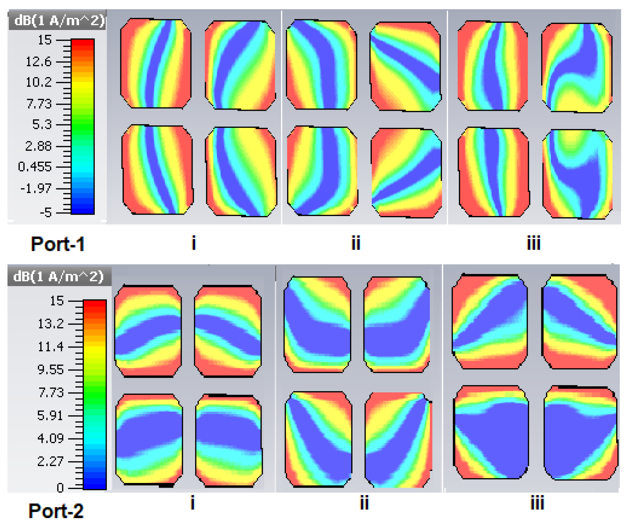
4.3. Gain and Current Distributions

The measured gains of the WBMA are presented in Figure 15. It is seen that the measured gains fluctuate with the highest of more than 6 dBi. Generally speaking, due to the wider operational bandwidth, the gains have more variations with respect to frequency.
The simulated current distributions on the wideband MIMO antenna at several frequencies are presented in Figure 16. On the parasitic patches, the current is mainly distributed along the edges of the slots. The left–right asymmetry of these patterns confirms that the antenna is capable of supporting multiple resonant modes whose overlapping leads to the wideband characteristic. Because the parasitic patches are offset only in the x direction (along the feedline axis), the current patterns remain almost symmetric about this axis.

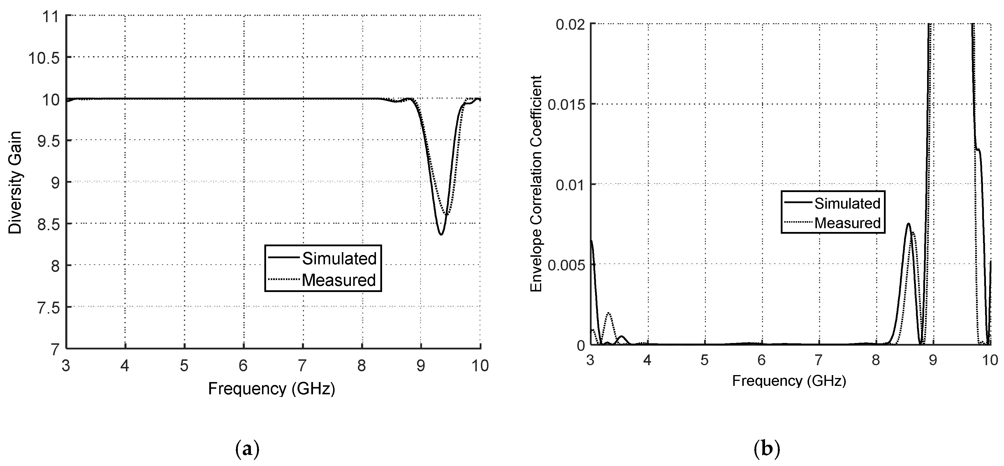
4.4. Diversity Gain, Correlation and Multiplexing Efficiency

The two feeds in the prototype antenna can be used to yield different polarization states. The basic intended function of the completed double array would be diversity reception, which is less complex than MIMO. This requires discrimination between the two orthogonal patterns and this can be represented as diversity gain, which can be computed from the radiation pattern: this is shown in Figure 17a. The average diversity gain is approximately 10 dB because the antenna has very low envelop correlation coefficient (ECC), as shown in Figure 17b.
Antenna envelope correlation between the two subarrays must be very low for the complete array to be viable for MIMO applications. For the design shown in Figure 1, the antenna envelope correlation found by simulation is presented in Figure 17b and it is seen that its value is almost zero across the intended wideband band. A similar result was found with the orthogonal configuration in Figure 2.
Another important parameter for MIMO is the multiplexing efficiency metric [45], defined as the difference in power required for a wideband MIMO antenna to deliver a given capacity in comparison with an ideal reference MIMO antenna, having zero correlation and 100% overall efficiency. For the antenna design in Figure 1, the multiplexing efficiency metric is shown in Figure 17a, which indicates that the proposed design is mainly limited by the overall efficiencies of the elements.

4.5. Performance Comparison

Table 4 shows the performance of the proposed antenna compared with other published stacked patch antennas [36,46,47,48,49,50,51,52,53,54,55,56]. As can be observed, our work has attained a wider impedance bandwidth compared to others, except [56]. In terms of the antenna size, this work has a comparable size in terms of the width and length. The presented design also has reasonable antenna gain and acceptable isolation in comparison with other published works.

5. Conclusions

A novel design of a compact wideband antenna has been presented. This has two orthogonal subarrays, enabling it to be used for diversity reception and MIMO. The radiation patterns of each subarray were nearly omnidirectional into their respective half spaces over the majority of the operating bandwidth. The two subarrays are orthogonally polarized and it was found that there was excellent isolation between them, despite their close proximity. This exploitation of polarization discrimination allows a much more compact design than the use of spatial discrimination in basic realizations of MIMO. Because of the above and its small size, the design becomes an attractive candidate for a range of emerging applications including 5G and 6G mobile systems. In addition, an efficient antenna design optimization technique is presented that is applicable to various kinds of design cases.

Author Contributions

Conceptualization, O.A., N.A., B.L., and R.A.-A.; methodology, O.A., B.L., and C.H.S.; software, O.A. and B.L.; validation, O.A., N.A., C.H.S., A.U., R.A.-A., N.J.M., and P.S.E.; formal analysis, O.A., B.L., and N.J.M.; investigation, O.A., N.A., B.L., A.U., R.A.-A., and C.H.S.; resources, O.A., N.A., B.L., and R.A.-A.; data curation, O.A., B.L., and A.U.; writing—original draft preparation, O.A.; writing—review and editing, C.H.S., R.A.-A., N.J.M., and P.S.E.; visualization, O.A., N.J.M., C.H.S., and P.S.E.; supervision, B.L. and R.A.-A.; project administration, R.A.-A., B.L., and P.S.E.; funding acquisition, R.A.-A., B.L., and P.S.E. All authors have read and agreed to the published version of the manuscript.

Funding

This work is partially supported by the innovation program under grant H2020-MSCAITN-2016 SECRET-722424 and financial support from the UK Engineering and Physical Sciences Research Council (EPSRC) under grant EP/E022936/1.

Acknowledgments

We dedicate this paper to Peter Excell who passed away on the 13th of August 2020 for his outstanding work ethic and continued support.

Conflicts of Interest

The authors declare no conflict of interest. The funders had no role in the design of the study; in the collection, analyses, or interpretation of data; in the writing of the manuscript, or in the decision to publish the results.

References

  1. Vitturi, S.; Zunino, C.; Sauter, T. Industrial Communication Systems and Their Future Challenges: Next-Generation Ethernet, IIoT, and 5G. Proc. IEEE 2019, 107, 944–961. [Google Scholar] [CrossRef]
  2. Chettri, L.; Bera, R. A Comprehensive Survey on Internet of Things (IoT) Toward 5G Wireless Systems. IEEE Internet Things J. 2020, 7, 16–32. [Google Scholar] [CrossRef]
  3. Xu, R.; Gao, S.; Izquierdo, B.S.; Gu, C.; Reynaert, P.; Standaert, A.; Gibbons, G.J.; Bösch, W.; Gadringer, M.E.; Li, D. A Review of Broadband Low-Cost and High-Gain Low-Terahertz Antennas for Wireless Communications Applications. IEEE Access 2020, 8, 57615–57629. [Google Scholar] [CrossRef]
  4. Costanzo, A.; Masotti, D.; Fantuzzi, M.; Del Prete, M. Co-Design Strategies for Energy-Efficient UWB and UHF Wireless Systems. IEEE Trans. Microw. Theory Tech. 2017, 65, 1852–1863. [Google Scholar] [CrossRef]
  5. Ma, R.; Behdad, N. A Compact, Low-Cost, Ultrawideband Direction-Finding System: Techniques Suitable for Small-Aperture Designs. IEEE Antennas Propag. Mag. 2018, 60, 32–44. [Google Scholar]
  6. Yan, S.; Soh, P.J.; Vandenbosch, G.A.E. Wearable Ultrawideband Technology—A Review of Ultrawideband Antennas, Propagation Channels, and Applications in Wireless Body Area Networks. IEEE Access 2018, 6, 42177–42185. [Google Scholar] [CrossRef]
  7. Yadav, R.; Malviya, L. UWB antenna and MIMO antennas with bandwidth, band-notched, and isolation properties for high-speed data rate wireless communication: A review. Int. J. RF Microw. Comput. Aided Eng. 2020, 30, 1–25. [Google Scholar] [CrossRef]
  8. Home, P.P.; Khan, T.; Laskar, R.H. A state-of-art review on band-notch characteristics in UWB antennas. Int. J. RF Microw. Comput. Aided Eng. 2019, 29, 1–16. [Google Scholar]
  9. Nadeem, I.; Choi, D. Study on Mutual Coupling Reduction Technique for MIMO Antennas. IEEE Access 2019, 7, 563–586. [Google Scholar] [CrossRef]
  10. Zhang, S.; Lau, B.K.; Sunesson, A.; He, S. Closely-packed UWB MIMO/diversity antenna with different patterns and polarizations for USB dongle applications. IEEE Trans. Antennas Propag. 2012, 60, 4372–4380. [Google Scholar] [CrossRef] [Green Version]
  11. Liu, L.; Cheung, S.W.; Yuk, T.I. Compact MIMO antenna for portable devices in UWB applications. IEEE Trans. Antennas Propag. 2013, 61, 4257–4264. [Google Scholar] [CrossRef] [Green Version]
  12. Mohamed, I.; Abdalla, M.; Mitkees, A. Perfect isolation performance among two-element MIMO antennas AEU. Int. J. Electron. Commun. 2019, 107, 21–31. [Google Scholar] [CrossRef]
  13. See, C.H.; Hraga, H.I.; Noras, J.M.; Abd-Alhameed, R.A.; McEwan, N.J. Compact Multiple Input and Multiple Output/Diversity Antenna for Portable and Mobile Ultra-wideband applications. IET Microw. Antennas Propag. 2013, 7, 444–451. [Google Scholar] [CrossRef]
  14. Yoon, H.K.; Yoon, Y.J.; Kim, H.; Lee, C.H. Flexible ultra-wideband polarisation diversity antenna with band-notch function. IET Microw. Antennas Propag. 2011, 5, 1463–1470. [Google Scholar] [CrossRef]
  15. Lee, J.M.; Kim, K.B.; Ryu, H.K.; Woo, J.M. A compact ultrawide-band MIMO antenna with WLAN band-rejected operation for mobile devices. IEEE Antennas Wirel. Propag. Lett. 2012, 11, 990–993. [Google Scholar]
  16. Sharawi, M.S.; Khan, M.U.; Numan, A.B.; Aloi, D.N. A CSRR loaded MIMO antenna system for ISM band operation. IEEE Trans. Antennas Propag. 2013, 61, 4265–4274. [Google Scholar] [CrossRef]
  17. Wang, L.; Du, Z.; Yang, H.; Ma, R.; Zhao, Y.; Cui, X.; Xi, X. Compact UWB MIMO Antenna with High Isolation Using Fence-Type Decoupling Structure. IEEE Antennas Wirel. Propag. Lett. 2019, 18, 1641–1645. [Google Scholar] [CrossRef]
  18. Khan, M.S.; Iftikhar, A.; Shubair, R.M.; Capobianco, A.; Braaten, B.D.; Anagnostou, D.E. Eight-Element Compact UWB-MIMO/Diversity Antenna with WLAN Band Rejection for 3G/4G/5G Communications. IEEE Open J. Antennas Propag. 2020, 1, 196–206. [Google Scholar] [CrossRef]
  19. Alibakhshikenari, M.; Virdee, B.S.; Shukla, P.; See, C.H.; Abd-Alhameed, R.A.; Falcone, F.; Quazzane, K.; Limiti, E. Isolation Enhancement of Densely Packed Array Antennas with Periodic MTM-Photonic Bandgap for SAR and MIMO Systems. IET Microw. Antennas Propag. 2020, 14, 183–188. [Google Scholar] [CrossRef]
  20. See, C.H.; Abd-Alhameed, R.A.; Abidin, Z.Z.; McEwan, N.J.; Excell, P.S. Wideband Printed MIMO/Diversity Monopole Antenna for WiFi/WiMAX Applications. IEEE Trans. Antennas Propag. 2012, 60, 2028–2035. [Google Scholar] [CrossRef] [Green Version]
  21. Alibakhshikenari, M.; Virdee, B.S.; See, C.H.; Abd-Alhameed, R.A.; Falcone, F.; Limiti, E. High-Isolation Leaky-Wave Array Antenna Based on CRLH-Metamaterial Implemented on SIW with ±30° Frequency Beam-Scanning Capability at Millimeter-Waves. Electronics 2019, 8, 642. [Google Scholar] [CrossRef] [Green Version]
  22. Alibakhshikenari, M.; Virdee, B.S.; Shukla, P.; See, C.H.; Abd-Alhameed, R.; Khalily, M.; Falcone, F.; Limiti, E. Antenna Mutual Coupling Suppression Over Wideband using Embedded Periphery Slot for Antenna Arrays. Electronics 2018, 7, 198. [Google Scholar] [CrossRef] [Green Version]
  23. Rajagopalan, A.; Gupta, G.; Konanur, A.S.; Hughes, B.; Lazzi, G. Increasing channel capacity of an ultrawideband MIMO system using vector antennas. IEEE Trans. Antennas Propag. 2007, 55, 2880–2887. [Google Scholar] [CrossRef]
  24. Saleem, R.; Bilal, M.; Bajwa, K.B.; Shafique, M.F. Eight-element UWB-MIMO array with three distinct isolation mechanisms. Electron. Lett. 2015, 51, 311–313. [Google Scholar] [CrossRef]
  25. Soltani, S.; Murch, R.D. A compact planar printed MIMO antenna design. IEEE Trans. Antennas Propag. 2015, 63, 1140–1149. [Google Scholar] [CrossRef]
  26. Kim, J.; Ju, J.; Eom, S.; Song, M.; Kim, N. Four-channel MIMO antenna for WLAN using hybrid structure. Electron. Lett. 2013, 49, 857–858. [Google Scholar] [CrossRef]
  27. Li, H.; Xiong, J.; Ying, Z.; He, S.L. Compact and low profile co-located MIMO antenna structure with polarisation diversity and high port isolation. Electron. Lett. 2010, 46, 108–110. [Google Scholar] [CrossRef]
  28. Gallo, M.; Daviu, E.A.; Bataller, M.F.; Bozzetti, M.; Pardo, J.M.; Llacer, L.J. A broadband pattern diversity annular slot antenna. IEEE Trans. Antennas Propag. 2011, 60, 1596–1600. [Google Scholar] [CrossRef]
  29. Adamiuk, G.; Zwick, T.; Wiesbeck, W. Compact, dual-polarized UWB- antenna, embedded in a dielectric. IEEE Trans. Antennas Propag. 2009, 58, 279–286. [Google Scholar] [CrossRef]
  30. Zhao, F.; Zhang, W.; Han, L.; Han, G.; Yang, R. A wideband dual-polarized patch antenna fed with the aperture-coupled microstrip. Electromagnetics 2018, 38, 58–69. [Google Scholar] [CrossRef]
  31. Kang, L.; Li, H.; Wang, X.; Shi, X. Compact Offset Microstrip-Fed MIMO Antenna for Band-Notched UWB Applications. IEEE Antennas Wirel. Propag. Lett. 2015, 14, 1754–1757. [Google Scholar] [CrossRef]
  32. Mao, C.; Chu, Q. Compact Coradiator UWB-MIMO Antenna with Dual Polarization. IEEE Trans. Antennas Propag. 2014, 62, 4474–4480. [Google Scholar] [CrossRef]
  33. Garg, R.; Bhartia, P.; Bahl, I.J.; Ittipiboon, A. Microstrip Antenna Design Handbook; Artech House: Boston, MA, USA, 2001. [Google Scholar]
  34. Legay, H.; Shafai, L. New Stacked Microstrip Antenna with Large Bandwidth and High Gain. IEE Proc. Microw. Antennas Propag. 1994, 141, 199–204. [Google Scholar] [CrossRef]
  35. Nishiyama, E.; Aikawa, M.; Egashira, S. Stacked microstrip antenna for wideband and high gain. IEE Proc. Microw. Antennas Propag. 2004, 151, 143–148. [Google Scholar] [CrossRef]
  36. Katyal, A.; Basu, A. Compact and Broadband Stacked Microstrip Patch Antenna for Target Scanning Applications. IEEE Antennas Wirel. Propag. Lett. 2017, 16, 381–384. [Google Scholar] [CrossRef]
  37. Liu, B.; Aliakbarian, H.; Ma, Z.; Vandenbosch, G.A.; Gielen, G.; Excell, P. An efficient method for antenna design optimization based on evolutionary computation and machine learning techniques. IEEE Trans. Antennas Propag. 2013, 62, 7–18. [Google Scholar] [CrossRef] [Green Version]
  38. Santner, T.J.; Williams, B.J.; Notz, W.I. The Design and Analysis of Computer Experiments; Springer Series in Statistics; Springer: New York, NY, USA, 2013. [Google Scholar]
  39. Price, K.; Storn, R.M.; Lampinen, J. Differential Evolution: A Practical Approach to Global Optimization; Springer Natural Computing Series; Springer: Berlin, Germany, 2005. [Google Scholar]
  40. Liu, B.; Zhang, Q.; Gielen, G.G. A Gaussian process surrogate model assisted evolutionary algorithm for medium scale expensive optimization problems. IEEE Trans. Evol. Comput. 2013, 18, 180–192. [Google Scholar] [CrossRef] [Green Version]
  41. Danjuma, I.M.; Akinsolu, M.O.; See, C.H.; Abd-Alhameed, R.A.; Liu, B. Design and Optimization of a Slotted Monopole Antenna for Ultra-wide Band Body Centric Imaging Applications. IEEE J. Electromagn. RF Microw. Med. Biol. 2020, 4, 140–147. [Google Scholar] [CrossRef] [Green Version]
  42. Grout, V.; Akinsolu, M.; Liu, B.; Lazaridis, P.; Mistry, K.; Zaharis, Z. Software Solutions for Antenna Design Exploration: A Comparison of Packages, Tools, Techniques and Algorithms for Various Design Challenges. IEEE Antennas Propag. Mag. 2019, 61, 48–59. [Google Scholar] [CrossRef]
  43. Nelder, J.; Mead, R. A Simplex Method for Function Minimization. Comput. J. 1965, 7, 308–313. [Google Scholar] [CrossRef]
  44. Liu, B.; Irvine, A.; Akinsolu, M.; Arabi, O.; Ali, N.; Grout, V. GUI Design Exploration Software for Microwave Antennas. J. Comput. Des. Eng. 2017, 4, 274–281. [Google Scholar] [CrossRef]
  45. Tian, R.; Lau, B.K.; Ying, Z. Multiplexing efficiency of MIMO antennas. IEEE Antennas Wirel. Propag. Lett. 2011, 10, 183–186. [Google Scholar] [CrossRef] [Green Version]
  46. Li, W.T.; Hei, Y.Q.; Grubb, P.M.; Shi, X.; Chen, R.T. Inkjet Printing of Wideband Stacked Microstrip Patch Array Antenna on Ultrathin Flexible Substrates. IEEE Trans. Compon. Packag. Manuf. Technol. 2018, 8, 1695–1701. [Google Scholar] [CrossRef]
  47. Zhu, Q.; Yang, S.; Chen, Z. Modified corner-fed dual-polarized stacked patch antenna for micro-base station applications. Electron. Lett. 2015, 51, 604–606. [Google Scholar] [CrossRef]
  48. Bondarik, A.; Sjoberg, D. Gridded Parasitic Patch Stacked Microstrip Antenna with Beam Shift Capability for 60 GHz Band. Prog. Electromagn. Res. B 2015, 62, 319–331. [Google Scholar] [CrossRef] [Green Version]
  49. Belen, M.A. Stacked microstrip patch antenna design for ISM band applications with 3D-printing technology. Microw. Opt. Technol. Lett. 2019, 61, 709–712. [Google Scholar] [CrossRef]
  50. Kumar, A.; Gupta, N.; Gautam, P.C. Design Analysis of Broadband Stacked Microstrip Patch Antenna for WLAN Applications. Wirel. Pers. Commun. 2018, 103, 1499–1515. [Google Scholar] [CrossRef]
  51. Sarin, V.P.; Nishamol, M.S.; Tony, D.; Aanandan, C.K.; Mohanan, P.; Vasudevan, K. A Wideband Stacked Offset Microstrip Antenna with Improved Gain and Low Cross Polarization. IEEE Trans. Antennas Propag. 2011, 59, 1376–1379. [Google Scholar] [CrossRef]
  52. Klionovski, K.; Shamim, A. Back Radiation Suppression through a Semitransparent Ground Plane for a Millimeter-Wave Patch Antenna. IEEE Trans. Antennas Propag. 2017, 65, 3935–3941. [Google Scholar] [CrossRef] [Green Version]
  53. Kim, J.; Hong, S.K.; Kim, B. A shared-aperture S/X dual broadband microstrip antenna with one perforated patch. Microw. Opt. Technol. Lett. 2020, 62, 507–513. [Google Scholar] [CrossRef]
  54. Feng, B.; Li, L.; Cheng, J.; Sim, C. A Dual-Band Dual-Polarized Stacked Microstrip Antenna with High-Isolation and Band-Notch Characteristics for 5G Microcell Communications. IEEE Trans. Antennas Propag. 2019, 67, 4506–4516. [Google Scholar] [CrossRef]
  55. Yang, X.; Ge, L.; Wang, J.; Sim, C. A Differentially Driven Dual-Polarized High-Gain Stacked Patch Antenna. IEEE Antennas Wirel. Propag. Lett. 2018, 17, 1181–1185. [Google Scholar] [CrossRef]
  56. Klionovski, K.; Shamim, A. Physically Connected Stacked Patch Antenna Design with 100% Bandwidth. IEEE Antennas Wirel. Propag. Lett. 2017, 16, 3208–3211. [Google Scholar] [CrossRef] [Green Version]
Figure 1. The proposed antenna geometry: (a) wideband MIMO antenna dimensions, (b) feeding structure and location of the via, and (c) side view of the antenna.
Electronics 09 01307 g001
Figure 2. Alternative WBMA structure with the two subarrays assembled orthogonally.
Electronics 09 01307 g002
Figure 3. The wideband MIMO antenna stacked structure.
Electronics 09 01307 g003
Figure 4. Evolution design procedure of the proposed antenna from Stage 1 to Stage 5.
Electronics 09 01307 g004
Figure 5. The proposed antenna performance in a design evolution process, as depicted in Figure 4. (a) Reflection coefficient (S11); (b) gains.
Electronics 09 01307 g005
Figure 6. Predicted values of reflection coefficient (S11) with five different parasitic patch sizes.
Electronics 09 01307 g006
Figure 7. Predicted values of reflection coefficient (S11) with five different values of substrate height h1.
Electronics 09 01307 g007
Figure 8. Predicted values of reflection coefficient (S11) with varying patch spacing distance, d1.
Electronics 09 01307 g008
Figure 9. Reflection coefficient (S11) with different via (xvia) locations.
Electronics 09 01307 g009
Figure 10. The wideband MIMO antenna prototype (left) and far field measurement facility (right).
Electronics 09 01307 g010
Figure 11. Measured and simulated results. (a) S11 and S22, (b) S12 and S21.
Electronics 09 01307 g011
Figure 12. S parameters for antenna in orthogonal configuration.
Electronics 09 01307 g012
Figure 13. Simulated and measured co-polar (Eθ) radiation patterns (θ-cut at φ = 0) at 5.5, 6.5, and 7.5 GHz for Port 1 and Port 2, where (a), (b), and (c) are for Port 1 and (d), (e), and (f) are for Port 2.
Electronics 09 01307 g013aElectronics 09 01307 g013b
Figure 14. Simulated and measured cross-polar (Eφ) radiation patterns (θ-cut at φ = 90) at 5.5, 6.5, and 7.5 GHz for Ports1 & Port 2
Electronics 09 01307 g014
Figure 15. Gain plots at different frequencies.
Electronics 09 01307 g015
Figure 16. Simulated current distribution at i. 5.5 GHz, ii. 6.5 GHz, and iii. 7.5 GHz.
Electronics 09 01307 g016
Figure 17. MIMO performance. (a) Diversity gain and (b) envelope correlation coefficient.
Electronics 09 01307 g017
Table 1. Wideband MIMO antenna optimal design variables (all sizes in mm).
ParametersVariableDimension
Main Patch Widthw210
Main Patch Lengthl210
Separation between Parasiticsd11.68
Parasitic Patch Lengthw18.4
Parasitic Patch Widthl18.4
Antenna Widthly18.48
Antenna Lengthlx18.48
Corner Truncated Length of the Parasitic PatchΔs1.2
Corner Truncated Length of the Main PatchΔp2
Via wrt. Main Patch ctr.xvia−3.5
1st Layer Thicknessh13.048
2nd Layer Thicknessh21.28
3rd Layer Thicknessh30.813
Feeding Strip widthw31.1
Feeding Strip Lengthl320.45
Table 2. Explored ranges of the design variables (all sizes in mm).
Variablesl2w2l1w1d1xviaxport
Lower bound55550.5−90.25
Upper bound181820205925
Table 3. Best designs obtained in Stage 1 and Stage 2 (all in mm).
Variablesl2w2l1w1d1xviaxport
Stage 110.1410.6315.9710.791.21−3.0215
Stage 210.0710.018.418.401.68−3.5120.45
Table 4. Performance comparison of the proposed antenna.
ReferencesFrequency Band (GHz)Impedance BandwidthAntenna Size
(Width × Length)
Gain
(dBi)
Isolation
(dB)
[36]4.9 to 7.0535%0.36 λo × 0.39 λo6.0NA
[46]4.79 to 5.045.1%0.35 λo × 0.50 λo4.5NA
[47]2.5 to 2.77.7%0.67 λo × 0.67 λo828
[48]54 to 6721.5%0.62 λo × 0.60 λo8NA
[49]2.4 to 2.54.1%1.34 λo × 1.14 λo10NA
[50]2.16 to 2.8226.5%0.78 λo × 0.58 λo5.530
[51]3.73 to 5.7334.9%0.52 λo × 0.68 λo8.0NA
[52]27.0 to 35.025.8%0.8 λo × 0.8 λo818
[53]4.55 to 6.2831.95%0.91 λo × 0.91 λo6.2NA
[54]3.28 to 3.711.4%0.48 λo × 0.48 λo8.040
[55]2.31 to 2.8119.0%1.19 λo × 1.19 λo1135
[56]23.9 to 72.2100.3%0.8 λo × 0.8 λo5NA
This work4.5 to 8.561.54%0.27 λo × 0.27 λo618
λo is the lowest operating frequency; NA: not applicable, as the antenna is a single element.

